Tag Archives: Small Times Magazine

June 15, 2011 — XG Sciences, a Michigan State University (MSU) spinoff, formed a series of agreements with POSCO, a Korean steel producer. The aim is advancing graphene manufacturing and product development, based on XG Science IP.

XGnP Graphene Nanoplatelets from XG Sciences are inexpensive additives for plastics, electronic components, batteries, etc.

Under the agreements, POSCO will purchase a 20% share of XG Sciences, obtaining production licenses to manufacture and sell xGnP Graphene Nanoplatelets. POSCO and XG Sciences will further collaborate on energy storage, advanced materials and electronics product development.

POSCO recently announced plans to invest $30 billion to expand its overseas operations. Earlier this year, however, it withdrew a bid to acquire Norway’s Elkem, a maker of silicon for solar panels, due to a lack of anticipated benefits from possible investment.

XG Sciences’ other international partner in Asia is Hanwha Chemical. These two companies allow the startup to reach top electronics, automotive and manufacturing companies in Asia, said Michael Knox, CEO of XG Sciences, adding that Asia-based customers will also have a local graphene manufacturing source.

For more information about XG Sciences visit www.xgsciences.com

POSCO, in addition to being one of the world’s largest steel producers, operates a worldwide network of subsidiaries in energy, construction, logistics, mining and materials markets.

June 14, 2011 – Marketwire — NanoInk’s NanoFabrication Systems Division is launching a force sensor and levelling devices at the Nanotech Conference and Expo, part of TechConnect World. NanoInk will also be presenting on Dip Pen Nanolithography (DPN) advances.

Force sensing with 1D levelling launched with the NanoArrayer 3000, and is also available on NanoInk’s NLP 2000. Combined with automation software, it facilitates automated pen array levelling and surface plane correction. Wizards guide users for printing micro and nano-arrays of uniform features across an entire glass slide.

For 2D levelling, proprietary sapphire ball technology enables large 2D arrays of high density pens to be levelled without contacting the substrate. This avoids cross contamination or the need for a sacrificial substrate area.

"Chips will be able to be printed with over a billion features in the 50nm to 10um size scale with densities greater than the current 55,000 2D pen array," said Tom Warwick, NanoInk GM, NanoFabrication Systems Division. Proteomics and genomics are some of the suitable applications for this "massively parallel high density printed arrays of features with low coefficients of variation," he added.

NanoInk’s NLP 2000 System is a desktop nanofabrication system that allows rapid design and custom engineering of functionalized surfaces on the micro and nanoscale, using DPN to transfer minute material quantities over a large, environmentally controlled work area. Organic, inorganic, and biological molecules can be deposited via the direct write, tip-based lithography technique. Researchers can deposit multiple materials, rapidly patterning arbitrary micro-and nanoscale features.

Jason Haaheim, Ph.D., and a senior R&D engineer at NanoInk, will present "Advances in Direct-Write Nanoscale Deposition and Patterning" on Wednesday, June 15, at 1:50 p.m. in room 103 at the Nanotech Conference and Expo. The presentation will provide additional details on both 1D and 2D levelling. NanoInk will also demonstrate the NLP 2000 at booth #1818.

NanoInk Inc. specializes in nanometer-scale manufacturing and applications development for engineering, life sciences, pharmaceutical, and education industries. More information is available at: www.nanoink.net/divisions.html#NanoFabrication.

Subscribe to our MEMS Direct newsletter

June 14, 2011 — Department of Electronic and Electrical Engineering at UCL and the London Centre for Nanotechnology researchers have demonstrated an electrically driven, quantum dot laser grown directly on a silicon (Si) substrate, with a 1300nm wavelength suitable for telecommunications electronics.

Click to Enlarge

Silicon photonics — optical interconnects for use with silicon electronics — will enable electronics to handle larger quanitites of data than current copper interconnects. However, silicon has proven to have a difficult atomic structure for light sources. Semiconductor lasers provide high-efficiency, direct interfaces for silicon electronics and data modulation. Direct compound semiconductor laser material growth on silicon could spur silicon photonics. However, the crystal lattice constants differ significantly between silicon and compound semiconductors, causing dislocations in the crystal structure. This leads to low efficiency and short operating lifetime for semiconductor lasers.

The UCL group developed special layers to prevent dislocations from reaching the laser layer, and a quantum dot laser gain layer. They demonstrated the technique on an electrically pumped 1,300nm wavelength laser grown by direct epitaxy on silicon.

In a recent paper in Optics Express (Vol. 19 Issue 12, pp.11381-11386 (2011)) they report an optical output power of over 15mW/facet at room temperature.

In collaboration with device fabricators at EPSRC National Centre for III-V Technologies, the team demonstrated the first quantum dot laser on a germanium (Ge) substrate by direct epitaxial growth. The laser, reported in Nature Photonics , (DOI: 10.1038/NPHOTON.2011.120, 12 June 2011) is capable of continuous operation at temperatures up to 70C and has a continuous output power of over 25mW/facet.

Quantum dot gain layers improve tolerance to residual dislocations relative to conventional quantum well structures, said Dr Huiyun Liu, epitaxy research leader and Royal Society University Research Fellow in the UCL Department of Electronic and Electrical Engineering. "Our work on germanium should also permit practical lasers to be created on the Si/Ge substrates that are an important part of the roadmap for future silicon technology."

Future work will tackle combining the lasers with waveguides and drive electronics, furthering silicon photonics integration, added Professor Alwyn Seeds, Head of the Photonics Group in the UCL Department of Electronic and Electrical Engineering, Principal Investigator in the London Centre for Nanotechnology and Director of the EPSRC Centre for Doctoral Training in Photonic Systems Development.

Learn more at http://www.ucl.ac.uk/

June 13, 2011 – PRNewswire — MEMS supplier STMicroelectronics (NYSE:STM) debuted "FingerTip" technology, which enables a single-chip solution for capacitive touchscreens up to 10" diameter with multi-touch capability.

FingerTip shares its architecture with STM’s more familiar MEMS devices: a sensing element connected to a high-performance capacitance-sensing circuit. The analog front-end (AFE) detects variations of capacitance in atto-Farads (10-[18] F), protecting system operation from noise, which plagues touchscreens.

The display, the system, human touch, and battery chargers (especially cheap ones) all assault touchscreens with noise. Strong periodic noise (100V peak-to-peak and in the frequency range from 1kHz to 1MHz) generates false "finger touches" to an analog front-end in touchscreen systems. FingerTip’s 32-bit digital signal processing (DSP) engine eliminates charger noise effects without impacting accuracy, frame rate or power consumption, STM reports. It filters out display noise as well, from ‘in-cell’ and ‘on-cell’ display technologies.

STMicro’s analog capacitive interface IP, developed for MEMS sensors, is well suited to digital noise filtering, said Benedetto Vigna, GM, MEMS, Sensors and High Performance Analog Division.

ST’s new product family is under evaluation with major customers that will implement FingerTip technology with stylus-based "hand writing," 10" tablets, smartphones, and other touchscreen apps that require fast response, linearity and accuracy, and low power consumption in a small package.

STMicroelectronics provides semiconductors and MEMS. Further information on ST can be found at www.st.com.

Subscribe to our MEMS Direct newsletter

June 13, 2011 – PRNewswire — IBM (NYSE: IBM) Research scientists have demonstrated an integrated circuit (IC) fabricated from wafer-scale graphene, creating a broadband frequency mixer operating at frequencies up to 10 gigahertz (10 billion cycles/second).

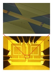
Click to EnlargeIBM was able to integrate graphene transistors with other components on a single chip, overcoming past challenges like poor adhesion of graphene with metals and oxides and unreliable fabrication processses. The IC combines a graphene transistor and a pair of inductors on a silicon carbide (SiC) wafer, fabbed with wafer-scale processes that maintained graphene quality.

Graphene was synthesized by thermal annealing SiC wafers to form uniform graphene layers on the wafer surface. Four metal layers and two oxide layers formed the top-gated graphene transistor, on-chip inductors and interconnects. The fabrication method can be applied to other types of graphene materials, including chemical vapor deposited (CVD) graphene films synthesized on metal films, and is compatible with optical lithography.

In 2010, IBM developed an epitaxially grown graphene transistor with 100GHz cutoff frequency. IBM noted at the time that their research was focused on process technologies compatible with silicon device fabrication. Much like the device announced today, the graphene transistor was grown on SiC with a top-gate structure.

Today’s analog graphene-based IC is designed for wireless communications, improving cellular operation at conventional frequencies; and for use at much higher frequencies to replace X-rays for military (weapons screening) and medical personnel (medical imaging). The circuit is a broadband frequency mixer, which produces output signals with mixed frequencies of the input signals for communications systems.

Single-layer, lattice-structured graphene could use less energy and cost less than conventional silicon-based devices in portable electronics. Its electrical, optical, mechanical and thermal properties promise better and new performance abilities. The new device boasts thermal stability to 125°C and frequency mixing to 10GHz.

The breakthrough is shared between IBM and the Carbon Electronics for RF Applications (CERA) program, funded by DARPA.

The graphene-based IC is highlighted in Science: http://www.sciencemag.org/content/332/6035/1294.short

The Binnig and Rohrer Nanotechnology Center opened at IBM Research – Zurich in May 2011. Learn more at http://www.ibm.com

By Debra Vogler, senior technical editor

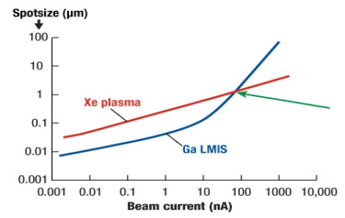
June 13, 2011 — FEI launched its Vion plasma focused ion beam (PFIB) system based on inductively-coupled plasma (ICP) source technology using a xenon ion beam. The system generates more than a micro-amp of beam current and can remove material faster (>20× improvements in speed, Fig. 1) than liquid metal ion sources that typically max out at a few tens of nano-amps, according to the company. Because of its speed, FEI will target new technologies, such as 3D packaging and 3D transistor design technologies, where PFIB analysis is more practical.

Click to Enlarge
  • High-volume milling/high beam current
  • Ga-FIB loses size advantage to plasma source as beam current goes above 50-60 nA
  • Xe has high sputter yield, high brightness, and low energy spread
  • No Ga contamination

Figure 1. Plasma FIB is 20× faster than current FIBs. Its fast ion milling capabilities enable rapid cross-sectioning of features from 50-1000µms. SOURCE: FEI

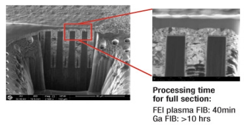
In a podcast interview, FEI product marketing manager Peter Carleson explained that gallium FIBs are already used for packaging applications, but with the cross-sections and trenches necessary for such applications (in the neighborhood of ~100µms), the removal process can take three, four, or even 8 hours. With the new source’s higher beam current, more samples can be done with greater tool utilization. The PFIB can also access lower regions of stacked dies to do traditional failure analysis or debugging (with the device "on") on the devices in the lower regions. The PFIB also enables quicker cross-sectioning of 3D integrated circuits that use TSVs/interposer layers (Fig. 2).

Click to Enlarge

Figure 2. High-speed sectioning of TSVs with plasma FIB. The device was located, cross-sectioned, polished, and imaged with PFIB. SOURCE: FEI

The product can perform site-specific removal of package and other materials to enable failure analysis and fault isolation on buried die; and circuit and package modifications to test design changes without repeating the fabrication process or creating new masks. Other applications include process monitoring and development at the package level, and defect analysis of packaged parts and MEMS devices.

Listen to the podcast:


  • Format: mp3
  • Length: 4:29
  • Size: 4.10 MB
  • Date: 06/13/11

June 10, 2011 — Fraunhofer Institute for Microelectronic Circuits and Systems IMS (Duisburg, Germany) developed a new etch process to manufacture micro electromechanical systems (MEMS) for commercial-scale applications. Etching gasses allow MEMS designers to use a wider range of materials for the functional layer, while preventing device damage during etch.

This isotropic etching is based on a substance that etches vertically into the MEMS substrate and tunnels under the functional layer. The result is a functional layer 100nm thin connected to the silicon or other substrate by certain suspension points.

Click to Enlarge

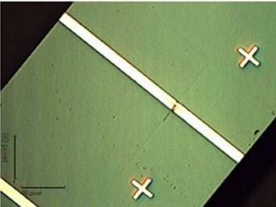
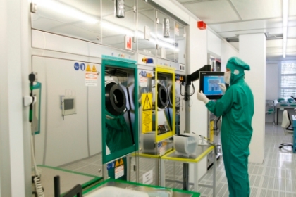
A researcher operates Fraunhofer’s MEMS production tools. Copyright Fraunhofer IMS.

Conventional etch is performed with liquids, and can only remove material vertically, said Dr. Marco Russ, project manager at IMS.  When the etch fluid dries, filigree membranes are stuck to the substrate or destroyed. Functional and sacraficial layer materials are limited by the etch liquid.

The group will open a MEMS production facility on June 22, incorporating the etch technology. The new facility will use 2 gases in the etch process chamber instead of liquids, Russ said: Hydrogen fluoride (HF), which strong etching properties on silicon dioxide but does not affect silicon; and xenon difluoride gas (XeF2), which acheives the opposite effect. The gasses allow greater materials flexibility.

Learn more at http://www.fraunhofer.de/en/

Also read: Deep silicon etching used for key MEMS building blocks by Trikon Technologies

Subscribe to our MEMS Direct newsletter

June 10, 2011 — The U.S. Department of Energy (DOE) will grant $2.9 million to Moser Baer Technologies (MBT) for work on better organic light emitting diode (OLED) manufacturing processes.

MBT aims to reduce the cost of manufacturing high-efficiency OLED lighting panels via improved processing steps. The research will focus on process control and cost reduction.

MBT has growing operations at the University of Albany’s College of Nanoscale Science and Engineering (CNSE) Smart System Technology & Commercialization Center of Excellence (STC). They will use CNSE STC’s pilot OLED production line to demonstrate and vet these manufacturing improvements. MBT is investing more than $17 million at CNSE’s STC for equipment for the pilot production line and creating 50+ high-tech jobs by 2013.

DOE is ponying up $15 million to support projects targeting LEDs and OLEDs, spending it on core research and development, new product development, and domestic manufacturing capacity. DOE is behind LEDs due to the energy savings LEDs can acheive over traditional lighting technologies.

US Senator Charles E. Schumer called OLEDs a driver for "good-paying private-sector jobs," as it brings Moser Baer into the western NY region.

The UAlbany CNSE is dedicated to education, research, development, and deployment of nanoscience, nanoengineering, nanobioscience, and nanoeconomics. Integrated into CNSE in a partnership of two of New York’s Centers of Excellence following a merger in September 2010, CNSE’s STC provides certified cleanroom space for fabrication and packaging of MEMS devices, and leverages CNSE’s $7 billion Albany NanoTech Complex, which features 80,000 square feet of Class 1 capable cleanrooms equipped with leading-edge tools and state-of-the-art capabilities. For information, visit www.cnse.albany.edu.

Moser Baer Technologies Inc. (MBT) is the U.S.-based subsidiary of Moser Baer India, Ltd., headquartered in New Delhi, and one of India’s leading technology companies. For more information, visit www.MoserBaer.com

June 9, 2011 – Marketwire — Boston Micromachines Corporation (BMC), which makes MEMS-based deformable mirror (DM) products for adaptive optics systems, won $1.2M in NASA contracts through NASA’s Small Business Innovation Research Program (SBIR). The Phase II contracts will expand on Phase 1, development of a reliable, fault-tolerant microelectromechanical deformable mirror (MEMS-DM) technology.

BMC won the Phase II contract based on technical merit and innovation, Phase I results, value to NASA, commercial potential and company capabilities, the company said in a statement.

BMC will design and fabricate a MEMS micromirror array of 1021 ultra-flat, close-packed hexagonal mirrors that can tip, tilt, and piston (TTP) with sub-nanometer precision. MEMS-DMs designs were successfully demonstrated in prior NASA work. The array, with 3 degrees of freedom and lambda/100 optical quality, will enable high-contrast visible nulling coronagraph instruments for exoplanet imaging.

BMC will also develop compact, ultra-low-power, high-voltage multiplexed drive electronics to support its MEMS-DMs in space-based wavefront control applications. In its Phase I award, BMC demonstrated a drive electronics approach that inherently limits actuator electrical current density generated to prevent permanent failure when a short time frame single fault failure occurs. This project will scale up BMC’s DM driver circuit developed for NASA on another project (Terrestrial Planet Finder Mission). NASA and BMC expect tenfold size and power reductions and decreased interconnection complexity.

NASA’s extra-solar planetary search will rely on high-resolution wavefront correction with deformable mirrors in telescopes, said Paul Bierden, president and co-founder of Boston Micromachines. Space-based telescopes have become indispensible in advancing the frontiers of astrophysics.

The awards were part of NASA’s Small Business Innovation Research programs.

Boston Micromachines Corporation (BMC) makes advanced microelectromechanical systems (MEMS)-based mirror products for use in commercial adaptive optics systems. By applying wavefront correction to produce high resolution images, BMC devices can be used for imaging biological tissue and the human retina and to enhance images blurred by the earth’s atmosphere. The company’s suite of compact deformable mirror (DM) products is cost effective and high performance. For more information on BMC, please visit www.bostonmicromachines.com.

Subscribe to our MEMS Direct newsletter

June 09, 2011 – Enhanced Online News — Kaiam Corporation, high-performance photonic IC maker, closed its Series B investment round with over $5 million. TriplePoint Capital, which led the round, cited Kaiam’s MEMS-based optical integration as "applicable as much for high-end high-capacity data transport as for low cost FTTH applications."

TriplePoint Capital was joined by existing investor U.S. Venture Partners (USVP). This equity investment approximately equals the amount commercial partners have provided for product development.

Kaiam will use the funds to ramp its initial products to volume manufacturing, and build out related infrastructure.

Jim Labe, TriplePoint Capital, said datacom and telecom sectors have an "unmet need" for optical ICs, and called Kaiam’s MEMS-based optical integration "a platform technology applicable as much for high-end high-capacity data transport as for low cost FTTH applications." He added that customer and commercial demand for Kaiam’s initial products pointed to the company as a good investment.

Kaiam Corporation develops products based on photonic integrated circuits (PICs). For more information, visit www.kaiamcorp.com.

TriplePoint Capital is a global specialty finance company serving high-growth private equity and venture-capital-backed companies. For more information, visit www.triplepointcapital.com.

Also read: Electronic + photonic + MEMS chip

Subscribe to our MEMS Direct newsletter