Tag Archives: Small Times Magazine

by Jan Provoost, science editor, imec Click to Enlarge

May 26, 2011 – At imec’s technology forum, Eric Dy, business development manager at imec, talked about the opportunities that advanced electronics can create in healthcare — to improve the efficiency and cost of the current medical practice, but also opportunities for new, disruptive research and treatments.

Currently, 70% of the diagnostic decisions are based on the results of lab tests. Molecular diagnostics often involves labor-intensive work with expensive machines. Considering the results of R&D work in imec and other research centra on labs-on-chip, there is a huge opportunity here to replace some of the tasks in the labs with mass-produced point-of-care equipment that give immediate feedback.

Going a step further: if we can mass-produce microdevices for molecular diagnostics, then the medical community will have access to a large amount of data that they can use to develop more predictive and personal treatments. Treatments that are based on cheap, personal molecular diagnostics.

imec is one of the few research centres where all the expertise and abilities needed to create the next wave of e-health comes together, Dy pointed out. Innovative circuit design, biosensors, wireless R&D, low-power ICs, biointerfacing — all are present, connected in an R&D ecosystem including such stakeholders as hospitals and medical device manufacturers.

Dy also showcased some of the technologies that will benefit the medical research community. One of the highlights is interfacing between biology and electronics. An example is a platform for high-content screening of molecules and tissues, consisting of an IC with a surface that allows cells to attach and grow, and to communicate through microsized electrodes with the underlying circuitry. Electronics as these will, according to Eric Dy, "help scientists do research that was not possible to do before."

CMOS chip with micronail electrode array for single-
cell stimulation and recording. (Source: imec)

by Els Parton, science editor, imecClick to Enlarge

May 26, 2011 — Nanoelectronics is not only about smaller transistors and more complex chips, it’s about a whole new world of opportunities and solutions to major societal challenges, underlined Luc Van de hove, president and CEO of imec, in his opening keynote at the organization’s annual technology forum.

A world of opportunities lies open for the semiconductor industry in the development of smarter and more user-friendly smartphones — 4.5 billion cell phones are in use today. This small device has altered the way we communicate and interact with our environment; it complements our senses with location information and omniscience. "One of the senses missing today is smell. Why not incorporate an electronic nose in future smart phones to check air quality, food freshness, or to perform alcohol tests," he asked, while showing a recent e-nose prototype based on MEMS.

Another key driver for the industry is the tablet PC. Market analysts predict that by the end of 2011, 54 million tablet PCs will be on the market. As many as 80 different tablet PCs were presented at the Consumer Electronics Show in Las Vegas.

3D TV is another major technology driver for the coming years. It will augment our user experience. The market shows an amazing growth rate of 80.2% with about 78 million devices expected by 2012. "Developments around holographic displays are very important in this field," Van den hove explained. Imec aims to design the ultimate 3D display: a holographic display with a 60-degree diffraction angle and a high-definition visual experience, based on NEMS technology," he noted.

And then there is organic electronics, enabling a whole new world of opportunities for ultralow-cost electronics: smart signage interacting with the environment, smart shopping displays suggesting people what to buy, and flexible light panes to stick anywhere in your home.

But nanoelectronics will also have its impact outside of information and communication technologies — e.g. on the healthcare sector, stated Van den hove. The first wave of health-based devices is on the market today assisting people during sports — however, the real challenge is to provide solutions for the aging population and the associated increasing healthcare cost," he said. "The second wave in health-based devices will be about ambulatory monitoring, bringing the doctor to your home."

And finally, there is the huge potential on the energy market to provide people with renewable energy solutions. "Of all sources of renewable energy, the sun has by far the largest potential," Van den hove said. The aim is to improve the yield of silicon PV systems, bringing down the cost per kilowatt-hour. This can be done by increasing the efficiency of the cells, using less base materials, increasing the lifetime of solar modules and by making the modules "smart" by integrating sensor functionalities. Meanwhile, organic PV will enable entirely new PV-integrated applications thanks to its flexible, low-cost and light-weight nature, he added.

From the multitude of trends and technology highlights that Van den hove showed during his presentation, one thing is clear: a world of opportunities lies ahead of us, both as a consumer and as an industrial player.

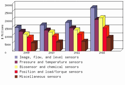
May 26, 2011 — BCC Research estimates that the sensors industry will be worth $91.5 billion in 2016. According to the research firm’s report, "Sensors: Technologies and global markets (IAS006D)," the sensors rise will translate to a five-year compound annual growth rate (CAGR) of 7.8%.

Click to Enlarge
Figure. Global sensors market, 2009-2016 in $ millions. Source: BCC Research May 2011.

Image, flow, and level sensors will grow at 8.5% CAGR to $27.2 billion in 2016, after being valued at $18.1 billion in 2011. This is considered the largest segment of the sensors market.

The second-largest segment, pressure and temperature sensors, equals roughly $14.5 billion in 2011. Expect to see that grow at 6.7% CAGR to nearly $20 billion in 2016.

Biosensors and chemical sensors are at $13.3 billion in 2011, and should hit $21 billion if the segment follows its projected 9.6% CAGR.

Position and load/torque sensors are worth $10.7 billion today. By 2016, 6.5% CAGR will drive the expected value to $14.7 billion.

The remaining "miscellaneous" sensors make up $6.1 billion of the overall sensors market. BCC Research forecasts a 6.7% CAGR through 2016.

Sensors are diversified into a range of end-use industries and products. BCC Research’s report takes into consideration various applications, sensor development and production technologies, and major market trends in terms of region and application sector. The report highlights new sensor developments with respect to continuous improvements in environmental performance.

To learn more, contact BCC Research (http://www.bccresearch.com), 35 Walnut Street, Suite 100, Wellesley, MA; Telephone: 866-285-7215

Follow Small Times on Twitter.com by clicking www.twitter.com/smalltimes. Or join our Facebook group

May 25, 2011 – JCN Newswire — Specialty foundry TowerJazz will collaborate as a manufacturing partner with Singapore’s Institute of Microelectronics (IME), an institute of the Agency for Science, Technology and Research (A*STAR) on micro-electro-mechanical systems (MEMS), packaging and ASICs. This marks another notch in TowerJazz’s Asia expansion, which includes new China offices and a potential fab buy in Japan.

TowerJazz is IME’s manufacturing partner in a three-party collaboration framework (the third party are fabless and fab-lite members). To-date, the collaboration has covered pressure sensors, inertial sensors, and micromirrors with MEMS companies. Through-silicon via (TSV) and advanced packaging, 3D IC, photonics, and nanoelectronics could drive future projects.

Existing CMOS fabrication processes can be implemented in MEMS manufacturing to bring costs down, and lead to more integration with CMOS devices, said Prof. Dim-Lee Kwong, executive director, IME. IME is an 8" (200mm) wafer technology development site for MEMS and ASICs.  MEMS fab integration into high-volume CMOS manufacturing facilities, and the promise of monolithic integration of CMOS + MEMS, could lower production costs on devices with both electronics and electromechanical functionalities.

Integrated CMOS + MEMS devices include airbag-sensor accelerometers and motion-control accelerometers in handheld gaming devices, high-performance switches for communications, fluidic devices in inkjet printer heads, and micromirrors for digital light projection (DLP, as in TVs). These four examples include highly diverse physics for the MEMS sensor, spanning mechanical motion sensing, tuning of high speed radio frequencies, actuation of fluidic valves, and optical reflection and tuning, respectively.

In addition to this Singapore-based collaboration, TowerJazz recently expanded in China, citing RF customers in the region, well as power management, CMOS image sensors (CIS), MEMS and other applications. TowerJazz is also considering buying Micron Technology’s semiconductor wafer fabrication facility in Nishiwaki City, Hyogo, Japan.

The Institute of Microelectronics (IME) is a research institute of the Science and Engineering Research Council of the Agency for Science, Technology and Research (A*STAR). *STAR supports Singapore’s key economic clusters by providing intellectual, human and industrial capital to its partners in industry. It also supports extramural research in the universities, hospitals, research centres, and with other local and international partners. For more information, visit IME on the Internet: http://www.ime.a-star.edu.sg.

Tower Semiconductor Ltd. (NASDAQ: TSEM, TASE: TSEM) is a global specialty foundry. TSEM and its fully owned U.S. subsidiary Jazz Semiconductor operate collectively under the brand name TowerJazz, manufacturing integrated circuits with geometries ranging from 1.0 to 0.13-micron. For more information, please visit www.towerjazz.com.

Follow Small Times on Twitter.com by clicking www.twitter.com/smalltimes. Or join our Facebook group

May 25, 2011 — The University of Virginia, in partnership with the College of William & Mary and Old Dominion University, has launched the Virginia Nanoelectronics Center (ViNC) for nano-electronics research. The ViNC will operate under the U.Va. Institute for Nanoscale and Quantum Scientific and Technological Advanced Research (nanoSTAR).

Top researchers will develop advanced materials, novel devices and circuits at nanoscale dimensions here. An important aspect of ViNC researchers’ work will be the discovery and development of materials for advanced information technologies. ViNC will develop novel devices and circuits for "beyond CMOS" nanoelectronics.

The center’s initial project will be to develop information processing based on vanadium dioxide, aiming for smaller and faster processing at much lower power than available technologies. 

Click to Enlarge

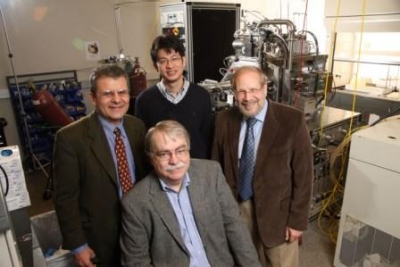
Clockwise from left: Mircea Stan, professor of electrical and computer engineering; Jiwei Lu, research assistant professor of materials science and engineering; Stuart Wolf, ViNC director and professor of materials science and engineering and physics, Lloyd Harriott, professor in the Department of Electrical and Computer Engineering.

Micron Technology, which owns a memory chip fab in Manassas, VA, helped the universities launch the nanotechnology center. Micron has a long-term research partnership with the University of Virginia, said Scott DeBoer, Micron VP of process research and development, citing the school’s next-generation memory and logic switch technologies research under nanoSTAR, the Virginia Microelectronics Consortium, and the Nanoelectronics Research Initiative.

This center grew, in part, from an earlier project, "Towards Establishment of an Industry-State-Federal National Center in Nanoelectronics," funded by the Commonwealth Research Commercialization Fund (previously known as the Commonwealth Technology Research Fund) and Micron Technology. The initiative is funded by major semiconductor companies, Micron Technology, Intel, IBM, Texas Instruments and GLOBALFOUNDRIES, as well as the National Institute of Standards and Technology. The Nanoelectronics Research Initiative, one of three research program entities of the Semiconductor Research Corporation (SRC), supports the center, with help from the commonwealth of Virginia through the Virginia Microelectronics Consortium, an industry-university, state-funded consortium to promote microelectronics in Virginia.

"This center could establish the [Virginia] as the ‘Oxide Hills’ rather than a new Silicon Valley," said Stuart Wolf, director of nanoSTAR and ViNC.

Wolf, a professor with joint appointments in the U.Va. Engineering School’s Department of Materials Science and Engineering and in the College of Arts & Sciences’ Department of Physics, previously worked for more than 12 years with the Defense Advanced Research Projects Agency (DARPA), where he directed funding of more than $200 million for computing research projects.

Wolf will work closely with co-principal investigators Jiwei Lu, assistant professor of materials science and engineering, and Mircea Stan and Lloyd Harriott, professors in the Department of Electrical and Computer Engineering. Ale Lukaszew from the College of William & Mary and Helmut Baumgart from Old Dominion University will also serve as co-principal investigators. 

The center is being established with starting grants from the Nanoelectronics Research Initiative and the Virginia Microelectronics Consortium and matching funds from the three participating universities, for a total of nearly $1.7 million over two years. The center’s projects are also funded by National Science Foundation and the Defense Advanced Research Projects Agency.

Follow Small Times on Twitter.com by clicking www.twitter.com/smalltimes. Or join our Facebook group

May 25, 2011 — STMicroelectronics (NYSE:STM), consumer and portable MEMS supplier, will bump up its micro electro mechanical systems (MEMS) production capacity to more than 3 million sensors a day by year’s end.

The capacity ramp is being supported by a "beefed-up manufacturing machine," said Benedetto Vigna, group VP and GM of ST’s MEMS, Sensors and High Performance Analog Division, citing the company’s high-volume fab capability and repeatable, consistent test procedure. ST Micro makes MEMS in Agrate and Catania, Italy (sensor fabrication), Rousset and Crolles, France (logic die production), and Kirkop, Malta and Calamba, Philippines (assembly and testing).

The company’s THELMA (Thick Epi-Poly Layer for Microactuators and Accelerometers) surface micro-machining process combines variably thick and thin poly-silicon layers for structures and interconnections (used in accelerometer and gyroscope MEMS fab). The complementary VENSENS (Venice Sensor) process allows STM to integrate a cavity into mono-crystalline silicon, producing an ultra-compact pressure sensor.

STMicroelectronics plans to sell these MEMS into high-growth markets as healthcare, industrial and automotive. STM began producing MEMS on 8" wafers in 2006, reducing its unit costs and accelerating development of new MEMS markets and expansion in established ones. STM’s MEMS sensors are used in smart phones, tablets, personal media players, game consoles, digital still cameras and remotes, as well as laptop computers, car airbags, and enhanced navigation systems.

STMicroelectronics provides semiconductors for multimedia convergence and power applications. Further information on ST can be found at www.st.com.

Follow Small Times on Twitter.com by clicking www.twitter.com/smalltimes. Or join our Facebook group

May 25, 2011Newport Corporation, lasers and photonics technology provider, introduced the Laser µFAB tabletop laser microfabrication workstation for researchers. Equipped with submicron resolution and a large stage, the tool can perform polymerization and ablation for MEMS, microelectronics, and other applications.

Click to EnlargeThe Laser µFAB is designed for use in additive and subtractive processes, including two-photon polymerization (TPP) during 3D microfabrication, laser ablation and surface structuring of various materials, volumetric writing, and nanosurgery/microdissection. Researchers use TPP to develop photoresists for photonics, microelectronics, and MEMS. The tool ablates and structures metals, polymers, semiconductors, glasses, ceramics, and biological targets. Waveguides and microfluidics can be volumetrically written in glass or polymer substrates.
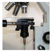
The Laser µFAB can be configured for use with femtosecond laser oscillators, amplifiers, OPAs, and other types of lasers in the visible to near-infrared (VIS-NIR) range. Sub-micron spot sizes are achieved at the sample with high numerical aperture (NA) objectives. Simple lenses can be used in applications where larger (10-20µm) spot sizes are acceptable. Computer-controlled variable attenuation integrated with the workstation prevents over or under exposure at the sample.

The standard Laser µFAB’s high-precision stages cover 100mm X/Y and 4.8mm Z, with 50nm resolution. This allows for continuous large area patterning without stitching. The top plate’s holder accomodates wafers, slides, cover slips, and other large samples.

Newport Corporation is an advanced-technology products and systems supplier to scientific research, microelectronics manufacturing, aerospace and defense/security, life and health sciences and precision industrial manufacturing markets. For additional information, visit www.newport.com/TAC-PR01

Follow Small Times on Twitter.com by clicking www.twitter.com/smalltimes. Or join our Facebook group

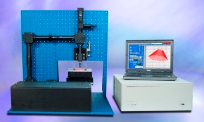
Click to EnlargeMay 24, 2011 — Sunrise Optical LLC debuted the Zebraoptical low coherence fiber optic interferometer with microscope attachment. The Zebraoptical Integrated Metrology Tool (ZIMT) provides metrology readings on micro electromechanical system (MEMS) wafers.
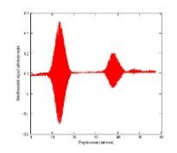
The tool’s standard Zebra wafer thickness and wafer topography metrology (ZebraOptical CT-IR) is paired with an optical microscope and VIS/NIR spectrometer. Users can measure substrate, membrane, and coating thicknesses and characterize coatings’ optical properties on the same tool platform.

A sample measurement service is available now. Learn more by contacting [email protected]. Lead time is currently 1 to 3 weeks ARO for the basic configuration.

Sunrise Optical LLC is an optical metrology company specializing in design and manufacturing of spectroscopic and imaging systems. www.zebraoptical.com.

Click to Enlarge
Zebraoptical Integrated Metrology Tool (ZIMT) interferometry measurement.

Follow Small Times on Twitter.com by clicking www.twitter.com/smalltimes. Or join our Facebook group

May 24, 2011 — Analog Devices Inc. (ADI) released the ADXL206 high precision, low power, dual-axis iMEMS accelerometer with signal conditioned analog voltage outputs. "Instead of using additional temperature compensation circuitry, ADI’s design techniques ensure that high performance is built into the microelectromechanical system (MEMS)," said Wayne Meyer, marketing and applications manager, MEMS/Sensors Technology Group, Analog Devices.

Because of the designed-in temperature compensation, quantization error and non-monotonic behavior are essentially eliminated, and temperature hysteresis is typically less than 2mg over the entire -40° to +175°C temperature range, said Meyer.

The single-chip ADXL206 measures acceleration with a full-scale range of ±5g and measures both dynamic acceleration such as tilt and static acceleration such as gravity. Offering a guaranteed operating temperature range of -40° to +175°C and excellent overall stability, the ADXL206 is well suited for geological downhole tools and other extreme high-temperature industrial applications. The ADXL206 MEMS device is compact, with lower power consumption (from over 10 to under 0.5mA per axis), enabling more information collection in constricted downhole regions.

The ADXL206 iMEMS accelerometer has a typical noise floor of 110 μg/√Hz, allowing signals below 1mg (0.06° of inclination) to be resolved in tilt sensing devices using narrow bandwidths (<60 Hz). 0.5-2.5kHz bandwidths can be selected to suit the application.

ADXL206 iMEMS accelerometer features:

  • -40° to +175°C temperature range
  • 1 mg resolution at 60Hz
  • Low power: 700μA at VS = 5V (typical)
  • High zero g bias repeatability
  • High sensitivity accuracy
  • 3500 g shock survival
  • 13 × 8 × 2mm, 8-lead, side-brazed ceramic dual in-line package (SBDIP) package

ADI also produced the AD8229, 1.0-nV/√Hz high-temperature instrumentation amplifier for high-temperature applications.

Analog Devices recently won a US International Trade Commission (ITC) ruling that found that Knowles Electronics infringed ADI’s Wafer Anti-Stiction Application (WASA) patent, U.S. Pat. No. 7,364,942 on its MEMS microphone technology.

ADI is a leader in data conversion and signal conditioning technology. Download data sheets and view product pages at http://www.analog.com/ADXL206

Follow Small Times on Twitter.com by clicking www.twitter.com/smalltimes. Or join our Facebook group

May 23, 2011 — The MEMS Industry Group (MIG) is organizing the inaugural "MEMS in the Machine" DemoZone at SEMICON West, on Tuesday, July 12 from 12:45 to 2pm.

SEMICON West, hosted by SEMI, will take place July 12-14 in San Francisco.

MIG members will demo cool applications that rely on MEMS technology, like smartphones and video games, gesture-based IPTV controllers, and other working consumer applications built with MEMS inertial sensors, optical MEMS, micro-mirrors, silicon microphones and more. "New MEMS" — a sector comprising MEMS devices for mobile and consumer applications — will grow by 157.4% in 2011, according to IHS iSuppli.

MIG’s "MEMS in the Machine" DemoZone is a way to show the semiconductor industry compelling examples of MEMS in action, according to the organizers. MEMS are an emerging technology sector within the industry, and share some processes, materials, and packaging technologies with mainstream chips.

Maps of the DemoZone will be available for SEMICON West attendees, and the MEMS companies will have designated booth space to share information on the product and company.

For a sample list of products that integrate MEMS, check out the MEMS in the Machine page: http://www.memsindustrygroup.org/i4a/pages/index.cfm?pageid=3933

MIG will also host "The Future of MEMS: Solutions for Moving from a Niche to a Mainstream Business" on July 12 at 10:30am–12:30pm during the Extreme Electronics TechXPOT, in the South Hall of SEMICON West. Teledyne DALSA Semiconductor, GLOBALFOUNDRIES, imec, Sand9 and others will discuss bringing MEMS into the fast-ramp, high-volume mainstream.

During the NorthOne TechXPOT, 2-4:30pm on the 12th, MIG will present "Heterogeneous Integration with MEMS and Sensors." Panelists will cover the eco-system of integrating MEMS and ICs.

Learn more at www.memsindustrygroup.org

Follow Small Times on Twitter.com by clicking www.twitter.com/smalltimes. Or join our Facebook group