Tag Archives: Small Times Magazine

April 26, 2011 — Air Science introduced its Purair ECO line of energy-saving ductless fume hoods designed for chemical and particulate protection over a range of laboratory and industrial applications.

Development of the Purair ECO is in response to an increasing worldwide demand for safe, cost-effective and energy-efficient ductless containment cabinets that minimize stress on facility HVAC systems without compromising protection for personnel and the environment.

The Purair ECO is available with a choice of controllers including the company’s ECOair touchpad control with color display interface.

An optional BACnet network interface connects all cabinet control, monitoring and alarm functions to an open-source facility monitoring system. The system is based on an industry-wide, non-proprietary ASHRAE compliant protocol for green building management.

The Purair ECO is available in five standard sizes from 30" wide to 69" wide.

For complete details, visit www.airscience.com

Follow Small Times on Twitter.com by clicking www.twitter.com/smalltimes. Or join our Facebook group

April 25, 2011 – PRWeb — Si-Ware Systems (SWS) announced a novel Self Compensating Oscillator (SCO) technology, which produces an all-silicon oscillator that can achieve an overall frequency stability better than 100ppm over a temperature range of -20 to +70ºC.

The SCO is an all-silicon oscillator that does not require an external frequency reference for frequency generation, and instead generates its frequency from an internal LC oscillator. As the name implies, the SCO is self compensated and achieves its stability without the need for analog or digital compensation. The stability is achieved with a low-cost room temperature only (RTO) trimming routine.

The SCO can achieve a frequency stability of 25ppm over a temperature range of 0 to 70ºC, which is inclusive of initial accuracy and temperature, supply, and load variations. This stability is a breakthrough for all-silicon oscillator technology and allows for a viable alternative to quartz or silicon MEMS (SiMEMS) based oscillators.

A clock oscillator in any electronic system uses a mechanical resonator, typically quartz or hermetically sealed SiMEMS. A conditioning ASIC is packaged together with the resonator to achieve the required oscillator clock output. By generating its frequency via an internal LC oscillator, the SCO eliminates the need for a mechanical resonator and is a single silicon die. The SCO has the advantage of being lower cost versus mechanical resonator oscillators as well as being more robust to shock and vibration as there are no moving structures.

The SCO’s output frequency is factory programmable and can generate frequencies from 1MHz to 133MHz. Operating voltage can be set to 1.8V, 2.5V or 3.3V, with current consumption in the single-digit mA range for frequencies up to 100MHz. The noise performance of the SCO is very good – at 125MHz the period jitter is 2ps RMS and the phase jitter is 0.7ps RMS (integrated 1MHz to 20MHz).

The SCO is a miniature silicon die that can be packaged in plastic with industry standard footprints. Alternatively, the SCO can be packaged with other ICs, allowing these ICs to eliminate the external frequency reference. Additional clocking circuitry, such as frequency synthesizers, can be easily added to the SCO creating a highly integrated, single chip timing solution.

SWS is currently preparing samples of its SCO technology for delivery in Q2 2011 to interested partners.

Si-Ware Systems (SWS) is an independent fabless semiconductor company providing a wide spectrum of product design and development solutions, custom ASIC development and supply as well as standard products, using MEMS, Analog/Mixed-Signal and Radio Frequency (RF) Integrated Circuits (ICs) expertise. For more information, visit http://www.si-ware.com.

Follow Small Times on Twitter.com by clicking www.twitter.com/smalltimes. Or join our Facebook group

By Debra Vogler, senior technical editor

April 25, 2011 — Imec researchers will present a paper titled "Carbon nanotube interconnects: electrical characterization of 150nm CNT contacts with Cu damascene top contact" at the IITC 2011 Conference (May 9-12, Dresden, Germany).

Click to EnlargeDr. Marleen van der Veen, senior research scientist at imec discussed the research results and their significance in this podcast interview:  Download or Play Now

Van der Veen highlighted the process technologies and steps used to grow the carbon nanotubes (CNTs) and the properties and attributes of the multi-walled CNTs (MWCNT) that resulted (Fig. 1). As noted in the paper, the lower slope for the Al2O3 pre-coated CNT implies a three times better CNT resistivity than the SiO2-coated ones.

Figure 1. Single CNT contact hole resistance as a function of the contact height for CNT coated with SiO2 (solid line) and Al2O3/SiO2 (dotted line).

The researchers took the integration process for 300mm contacts and transferred it to 150nm contact holes compatible with the module for 130nm device technologies (Fig. 2). The researchers maintain that because CNTs grown from different recipes and processed under different conditions can be rapidly benchmarked, they believe that their work will be important for manufacturing CMOS-compatible CNT interconnects, as well as for improving CNT interconnect resistance in advanced CMOS interconnects.

a) 
b) 

Figure 2. SEM images from different stages of the integration in 150nm contact holes a) before damascene litho and b) after barrier deposition and Cu fill.


More IITC previews:

IBM IITC preview: BEOL interconnect tech for <22nm

Beyond ball shear test: Microprobing chip/package stress at Stanford

April 25, 2011 — A University of Arkansas physicist has received the largest award granted to an individual researcher from the Army Research Laboratory to search for a novel class of nanomaterials with rationally designed properties.

Physicist Jak Chakhalian seeks to create a new class of materials: topological insulators combined with magnetic and superconductivity properties within just a few atomic layers. The materials could enable topological quantum computers, which could break complex encryption codes and compute things beyond the power of today’s supercomputers.

"It will revolutionize the way we think about electrons moving in conventional insulators and metals even at the nanoscale," Chakhalian said. The Army Research Lab is funding his research with $1.2 million over five years.

Recently Chakhalian, associate professor of physics in the J. William Fulbright College of Arts and Sciences, and colleagues found that atomic orbitals change substantially at the interface between a ferromagnet and a high-temperature superconductor. This finding opens up a new way of designing nanoscale superconducting materials. It also fundamentally changes scientific convention, which suggests that only electron spin and atomic charge — not atomic orbitals — influence the properties of nanostructures.

Chakhalian wants to create a topological insulator as a nanostructure with magnetic and superconducting properties in a few atomic layers at the interface.

Chakhalian will use the grant from the Army Research Laboratory to build new equipment to create and test atomically thin superlattices by combining novel materials and using the interface as a tool.

Photo. Doctoral student Benjamin Gray, left, and Jak Chakhalian in the laboratory with a unique state-of-the-art piece of equipment built last summer to fabricate atomic layers of complex oxides.

This research was cited by Science as one of the top 10 research breakthroughs of 2007.

Until recently, researchers only recognized three fundamental types of materials: metals such as iron and gold, insulators and semiconductors. In 2006, theoretical physicists suggested that another completely unknown class of insulating materials might exist. This class, called topological insulators, would not conduct electricity inside the crystal but permits the perfect conduction on the surface within a single atomic layer. This happens because geometry protects the surface electrons. In 2007, scientists looked at the alloy bismuth telluride and found the properties that this theory predicted. They had discovered a new class of material.

"On the inside, bismuth telluride is an insulator, but on the surface, within one atomic layer, it’s a perfect conductor," Chakhalian said. "It will conduct within the single atomic layer no matter how disordered the crystal on the inside. This is a whole new class of materials very similar to the Nobel prize-winning material, graphene, with many other interesting twists."

Chakhalian is a member of the University of Arkansas Institute for Nanoscience and Engineering. He holds the Charles E. and Clydene Scharlau Endowed Professorship in Chemistry.

Learn more at http://www.uark.edu/home/

Follow Small Times on Twitter.com by clicking www.twitter.com/smalltimes. Or join our Facebook group

April 23, 2011 — Virginia Commonwealth University researchers have identified the molecular mechanisms at play for the non-additive wetting free energies at chemically heterogeneous surfaces.

Across disciplines, researchers have long wondered how best to predict hydrophobicity — a molecule’s resistance to wetting — of a mixed surface from the knowledge of its pure constituents. These findings provide insight into that basic physical phenomenon and can be used to predict and understand the energy cost to wet a surface, which may be applied to nanochemistry, materials science and biophysics. The study was published in the April 1 issue of the Proceedings of the National Academy of Sciences (http://www.pnas.org/content/108/16/6374.short).

Click to Enlarge

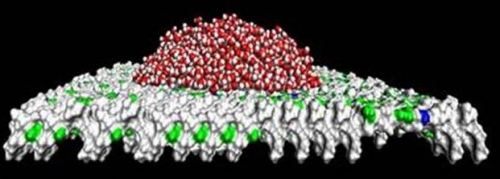
Image. Experiments in silico uncover molecular mechanisms of surface wetting: nanodroplet geometry used in calculation of water contact angle on flattened melittin, a natural nanopatterned surface. Image courtesy of Alenka Luzar, Ph.D.,/VCU.Sathya Achia Abraham, VCU Communications and Public Relations.

"The work addresses, via molecular-level simulations, a routine feature of macroscopic surface measurements done daily in experimental labs and shows that the observed results can be interpreted quite straightforwardly when the molecular scale features of surface topography, and a little chemistry, are considered," said principal investigator Alenka Luzar, Ph.D., a professor in the VCU Department of Chemistry.

According to Luzar, understanding the wetting of nanopatterned surfaces at a molecular level are important for everyday applications in materials science (inkjet printing, for example), and biology in protein hydration.

"Solvent access to distinct surface ingredients, in addition to the chemical composition, is key to the wettability of a heterogeneous material. This notion can guide computer-assisted design (CAD) of improved materials and helps explain the solubility and function of biomolecules in aqueous solution," she said.

The team demonstrated non-additivity of the cosine of contact angle, or the adhesion energy, on the fraction of hydrophobic/hydrophilic chemistries by measuring nano-droplet contact angles on model surfaces. They found these deviations to be positive, meaning the surface is more hydrophilic at a given fraction than previously predicted by linear expectation, or negative, meaning that the surface is more hydrophobic than previously predicted. Luzar said that the source of these effects can be traced down to size-asymmetry of distinct surface functionalities, as the more prominent groups hide the smaller ones.

Jihang Wang, Ph.D., a graduate student in Luzar’s research group, is the lead author on this paper, which is based on work done solely at VCU. Luzar also collaborated with Dusan Bratko, Ph.D., a professor with the VCU Department of Chemistry.

The study was supported in part by the National Science Foundation and U.S. Department of Energy.

Learn more at http://www.vcu.edu/

Also read: Accurate assessment of water quality for improved process control

Follow Small Times on Twitter.com by clicking www.twitter.com/smalltimes. Or join our Facebook group

Yole Développement released a new report, MEMS Microphone, presenting MEMS microphones technologies, the related supply chain and its key players. Yole Développement also analyses the MEMS microphones applications and markets including worldwide market metrics from 2010 to 2016 and market shares. What are the key technologies challenges? What will be the evolution of such market?

Micro electromechanical system (MEMS) microphones are already widely used in consumer applications (cell phones, laptops). More and more mobile phones are using 2 or more MEMS microphones for Active Noise Cancellation (ANC). Other consumer products such as laptops, camcorders etc. are using MEMS microphones arrays (2,4 or 6 microphones) for the multidirectional function.

"The mobile phone market is still the largest consumer of MEMS microphones. With the penetration of MEMS microphones in the iPhone 4 and other smart phones, Yole estimates rapid growth of the market in 2011-2016. By 2013, shipments will increase to over 1 billion units and more than 2 billion units by 2016," explains Wenbin Din, market analyst at Yole Développement, who authored the report.

Knowles is the market leader with more than 80% market share. Even though competitors are growing, such as AAC Acoustic Technologies, Hosiden and BSE, how to compete with Knowles remains the big question for the rest of the players in this industry.

More companies with new products will try to compete against Knowles, through new design, new packaging and new software enabling key functions. 2011 is a very important year with multiple launches of new devices by existing MEMS microphone companies: Analog Devices, Akustica, TDK-EPC, Wolfson Technologies, etc.

Companies cited in the report:

AAC Acoustic Technologies, Akustica/Bosch, Analog Devices, APM, Apogee, Apple, ASE, AudioPixels, Auxitrol, AvagoTech, B&K, BenQ, BSE, Continental, CSIL, CSMC-Tech, Draper Lab, Goertek, Google, GMEMS, Hosiden, Infineon, INN, Knowles acoustics, LG, Lingsen Pecision Industries, MEMSensing, MEMSTech, Merry electronics, Microflown, MosArt Packaging, Motorola, NASA, NCT, Nokia, NXP, Omron, Panasonic, Phone Or, Samsung, Siemens, Silicon Matrix, Solid State System, ST Microelectronics, Tong Hsing, TDK-EPC, Toshiba, UMC, VK mobile, VTT Electronics, Wolfson, Xfab, Yamaha

Infineon has turned into a microphone die supplier and works with Asian MEMS microphone players. Other companies are trying to become microphone manufacturers instead of just foundries (MEMSTech, for example). Some players say that it is just a step of transition to buy microphone dies from others.

The access to MEMS microphone original design will be more and more important in the future and we can expect both strong R&D projects and also M&A to get access to MEMS design and manufacturing capabilities. The Yole report offers a more in-depth discussion on this scope and key strategic evolution of the industry.

IP rights and packaging patents are critical for manufacturers to achieve performance and cost goals. This report will include a special focus here, describing recent disputes of main players.

Wenbin Din is responsible for MEMS market research at Yole Développement. She previously worked at research center CEA Grenoble (France). She holds a Microelectronics Engineering degree from the National Engineering School in Caen, plus a Master Degree in Business Administration from IAE Caen, France.

For more information on this report, visit http://www.i-micronews.com/reports/MEMS-Microphone/202

Follow Small Times on Twitter.com by clicking www.twitter.com/smalltimes. Or join our Facebook group

April 21, 2011 — A University of Pittsburgh-led team has created a single-electron transistor that provides a building block for new, more powerful computer memories, advanced electronic materials, and the basic components of quantum computers.

The researchers report in Nature Nanotechnology that the transistor’s central component, a 1.5nm-diameter island, operates with the addition of only one or two electrons. That capability would make the transistor important to a range of computational applications, from ultradense memories to quantum processors.

In addition, the tiny central island could be used as an artificial atom for developing new classes of artificial electronic materials, such as exotic superconductors with properties not found in natural materials, explained lead researcher Jeremy Levy, a professor of physics and astronomy in Pitt’s School of Arts and Sciences. Levy worked with lead author and Pitt physics and astronomy graduate student Guanglei Cheng, as well as with Pitt physics and astronomy researchers Feng Bi, Daniela Bogorin, and Cheng Cen. The Pitt researchers worked with a team from the University of Wisconsin at Madison led by materials science and engineering professor Chang-Beom Eom, including research associates Chung Wun Bark, Jae-Wan Park, and Chad Folkman. Also part of the team were Gilberto Medeiros-Ribeiro, of HP Labs, and Pablo F. Siles, a doctoral student at the State University of Campinas in Brazil.

Levy and his colleagues named their device SketchSET, or sketch-based single-electron transistor, after a technique developed in Levy’s lab in 2008 that works like a microscopic Etch A Sketch, the drawing toy that inspired the idea. Using the sharp conducting probe of an atomic force microscope (AFM), Levy can create such electronic devices as wires and transistors of nanometer dimensions at the interface of a crystal of strontium titanate and a 1.2nm-thick layer of lanthanum aluminate. The electronic devices can then be erased and the interface used anew.

The SketchSET, which is the first single-electron transistor made entirely of oxide-based materials, consists of an island formation that can house up to two electrons. The number of electrons on the island — zero, one, or two — results in distinct conductive properties. Wires extending from the transistor carry additional electrons across the island. An atomic-scale depiction of the SketchSET is available at http://www.news.pitt.edu/news/Levy_SketchSET_NatureNano.

One virtue of a single-electron transistor is its extreme sensitivity to an electric charge. Another property of these oxide materials is ferroelectricity, which allows the transistor to act as a solid-state memory. The ferroelectric state can, in the absence of external power, control the number of electrons on the island, which in turn can be used to represent the 1 or 0 state of a memory element. A computer memory based on this property would be able to retain information even when the processor itself is powered down, Levy said. The ferroelectric state also is expected to be sensitive to small pressure changes at nanometer scales, making this device potentially useful as a nanoscale charge and force sensor.

Since August 2010, Levy has led a $7.5 million, multi-institutional project to construct a semiconductor with properties similar to SketchSET, he said. Funded by the U.S. Air Force Office of Scientific Research’s Multi-University Research Initiative (MURI) program, the five-year effort is intended to overcome some of the most significant challenges related to the development of quantum information technology. Levy works on that project with researchers from Cornell, Stanford, the University of California at Santa Barbara, the University of Michigan, and UW-Madison.

The research in Nature Nanotechnology also was supported in part by grants from the U.S. Defense Advanced Research Projects Agency (DARPA), the U.S. Army Research Office, the National Science Foundation, and the Fine Foundation.

Follow Small Times on Twitter.com by clicking www.twitter.com/smalltimes. Or join our Facebook group

April 20, 2011 — Stanford researchers have developed a new biosensor microchip that could significantly speed up the process of drug development. The microchips, packed with highly sensitive "nanosensors," analyze how proteins bind to one another, a critical step for evaluating the effectiveness and possible side effects of a potential medication.

Image 1. A microchip with an array of 64 nanosensors. The nanosensors appear as small dark dots in an 8 x 8 grid in the center of the illuminated part of the backlit microchip. Courtesy of Sebastian Osterfeld

A single centimeter-sized array of the nanosensors can simultaneously and continuously monitor thousands of times more protein-binding events than any existing sensor. The new sensor is also able to detect interactions with greater sensitivity and deliver the results significantly faster than the present "gold standard" method.

"You can fit thousands, even tens of thousands, of different proteins of interest on the same chip and run the protein-binding experiments in one shot," said Shan Wang, a professor of materials science and engineering, and of electrical engineering, who led the research effort.

"In theory, in one test, you could look at a drug’s affinity for every protein in the human body," said Richard Gaster, MD/PhD candidate in bioengineering and medicine, who is the first author of a paper describing the research that is in the current issue of Nature Nanotechnology, available online now (http://www.nature.com/nnano/journal/vaop/ncurrent/full/nnano.2011.45.html).

The power of the nanosensor array lies in two advances. First, the use of magnetic nanotags attached to the protein being studied (medication, for example) greatly increases the sensitivity of the monitoring.

Second, an analytical model the researchers developed enables them to accurately predict the final outcome of an interaction based on only a few minutes of monitoring data. Current techniques typically monitor no more than four simultaneous interactions and the process can take hours.

Image 2. A microchip with a nanosensor array (orange squares) is shown with a different protein (various colors) attached to each sensor. Four proteins of a potential medication (blue Y-shapes), with magnetic nanotags attached (grey spheres), have been added. One medication protein is shown binding with a protein on a nanosensor. Courtesy of Richard Gaster.

Members of Wang’s research group developed the magnetic nanosensor technology several years ago and demonstrated its sensitivity in experiments in which they showed that it could detect a cancer-associated protein biomarker in mouse blood at a thousandth of the concentration that commercially available techniques could detect. That research was described in a 2009 paper in Nature Medicine.

The researchers tailor the nanotags to attach to the particular protein being studied. When a nanotag-equipped protein binds with another protein that is attached to a nanosensor, the magnetic nanotag alters the ambient magnetic field around the nanosensor in a small but distinct way that is sensed by the detector.

"Let’s say we are looking at a breast cancer drug," Gaster said. "The goal of the drug is to bind to the target protein on the breast cancer cells as strongly as possible. But we also want to know: How strongly does that drug aberrantly bind to other proteins in the body?"

To determine that, the researchers would put breast cancer proteins on the nanosensor array, along with proteins from the liver, lungs, kidneys and any other kind of tissue. The medication, with its magnetic nanotags attached, would bind with proteins in varying degrees. "We can see how strongly the drug binds to breast cancer cells and then also how strongly it binds to any other cells in the human body such as your liver, kidneys and brain," Gaster said. "So we can start to predict the adverse affects to this drug without ever putting it in a human patient." The next step is to use this microchip with a specific drug under development.

It is the increased sensitivity to detection that comes with the magnetic nanotags that enables Gaster and Wang to determine not only when a bond forms, but also its strength. "The rate at which a protein binds and releases, tells how strong the bond is," Gaster said. That can be an important factor with numerous medications.

The nanosensor is based on the same type of sensor used in computer hard drives, Wang said. "Because our chip is completely based on existing microelectronics technology and procedures, the number of sensors per area is highly scalable with very little cost," he said.

Although the chips used in the work described in the Nature Nanotechnology paper had a little more than 1,000 sensors per square centimeter, Wang said it should be no problem to put tens of thousands of sensors on the same footprint.

"It can be scaled to over 100,000 sensors per centimeter, without even pushing the technology limits in microelectronics industry," he said.

Wang said he sees a bright future for increasingly powerful nanosensor arrays, as the technology infrastructure for making such nanosensor arrays is in place today. 

Other Stanford researchers who participated in the research and are coauthors of the Nature Nanotechnology paper are Liang Xu and Shu-Jen Han, both of whom were graduate students in materials science and engineering at the time the research was done; Robert Wilson, senior scientist in materials science and engineering; and Drew Hall, graduate student in electrical engineering. Other coauthors are Drs. Sebastian Osterfeld and Heng Yu from MagArray Inc. in Sunnyvale. Osterfeld and Yu are former alumni of the Wang Group.

Funding for the research came from the National Cancer Institute, the National Science Foundation, the Defense Advanced Research Projects Agency, the Gates Foundation and National Semiconductor Corporation

Story courtesy of Louis Bergeron, Stanford University. http://www.stanford.edu/

Follow Small Times on Twitter.com by clicking www.twitter.com/smalltimes. Or join our Facebook group

April 20, 2011 — SmartKem Limited, developer of novel, printable organic semiconductor materials and ink formulations for flexible electronics, received investment funding from the Porton Capital Group and Finance Wales Investments Limited. The investment allows SmartKem to further develop its flexible printed electronics solutions.

Based in Denbighshire, Wales, SmartKem develops a novel range of high mobility organic semiconductor molecules and ink formulations compatible with printed electronic processes. This is an inexpensive, low weight, low energy, alternative to silicon semiconductors and can be used to print organic circuits and devices onto thin flexible substrates such as plastics and paper.

SmartKem has just completed a key R&D phase and is focusing on the formulation of innovative organic semiconductor inks for improved performance and manufacturing of printed transistor arrays and logic circuits. The company targets electronic displays, thin-film RFID, smart sensors and printed logic circuit integration. The funding puts SmartKem at a definitive position in the microelectronics market.

Steve Kelly, CEO SmartKem, comments, “Our semiconductor materials are currently being sampled to a number of electronic device manufacturers and with this investment, SmartKem can scale up market testing and accelerate towards commercialization. This will allow us to further establish our position as a leading independent provider of organic semiconductor solutions for the printed electronics sector and to continue our breakthrough research and development projects.”

SmartKem is a high tech enterprise developing an new technology focusing on high performance/high value organic semiconductor materials that can be printed to form electronic circuits onto lightweight, rugged and low cost polymer films. For more information on SmartKem, visit www.smartkem.com.

Follow Small Times on Twitter.com by clicking www.twitter.com/smalltimes. Or join our Facebook group

Update November 16, 2011 — Aurrion won the contract for the DARPA Electronic-Photonic Heterogeneous Integration (E-PHI) program to develop technologies and architectures to enable chip-scale electronic-photonic/mixed-signal integrated circuits on a common silicon substrate. Aurrion’s goal is to develop the necessary technologies, architectures, and design innovations to enable novel chip-scale electronic-photonic and mixed-signal integrated circuits on a common silicon substrate.

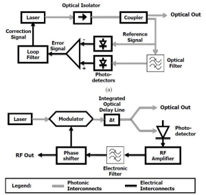
April 20, 2011 — Microelectronics scientists at the U.S. Defense Advanced Research Projects Agency (DARPA) in Arlington, VA, are reaching out to industry to find new ways of blending electronic, photonic, and micro-electro mechanical systems (MEMS) components on one silicon integrated circuit (IC).

The goal is to develop microelectronics technology for optoelectronic microsystems such as transceivers for telecommunications, coherent optical systems for laser radar (LADAR) sensors and communications, optical arbitrary waveform generators, and multi-wavelength imagers with integrated image processing and readout circuitry.

Click to Enlarge

The DARPA Microelectronics Technology Office (MTO) released a broad agency announcement (DARPA-BAA-11-45) late last week for the Electronic-Photonic Heterogeneous Integration (E-PHI) program to develop technologies and architectures to enable chip-scale electronic/photonic/mixed-signal integrated circuits on a common silicon substrate.

Technologies developed in the E-PHI program should provide considerable performance improvements and size reductions over current state-of-the-art technologies, DARPA officials say. Of particular interest are low-noise electronic/photonic signal sources in the 20GHz radio frequency (RF) band and in the 1,000 to 2,000nm near-infrared (IR) optical band. These technologies could improve optical gyroscopes, direction finding, optical communications, and frequency reference synchronization for advanced high-bandwidth RF and mixed signal chip-integrated systems, notes DARPA. DARPA scientists anticipate that integrating photonics and electronics on a silicon substrate could produce compact optical oscillators, faster electronic feedback, enhanced coupling among photonic components, and better thermal and vibration tolerance.

First, these technologies must be manufactured on existing silicon CMOS chip fabs. Examples of potential approaches include micro-assembly, epitaxial layer bonding and printing, and direct epitaxial growth in silicon process flows.

Companies interested should submit proposals by June 3, 2011.

For questions or concerns, contact DARPA’s Scott Rodgers by e-mail at [email protected]

More information is online at https://www.fbo.gov/spg/ODA/DARPA/CMO/DARPA-BAA-11-45/listing.html.

A proposer’s day to brief industry and providing teaming opportunities will take place May 2 in the Washington, D.C. area. Those interested in attending should register no later than April 27 by e-mail at [email protected].

The E-PHI is divided into three parts: heterogeneous electronic-photonic integration process and device technologies; heterogeneously integrated electronic/photonic architectures; demonstration microsystems. Industry proposals that address all three areas are of particular interest, DARPA officials say.

The aim of the first part is to develop fabrication and device technologies to integrate different photonic and optoelectronic materials on a silicon CMOS-compatible substrate. Modular approaches are of particular interest, DARPA officials say.

The second part focuses on architectures and design approaches that take advantage of heterogeneously integrated materials and electronic and photonic devices. The third part centers on demonstrating microsystems based on technologies and approaches developed in the first two parts of the E-PHI program — particularly continuous-wave and pulsed laser sources; RF optoelectronic signal sources; and other novel demonstration systems.

The E-PHI initiative is part of a larger DARPA program called Diverse Accessible Heterogeneous Integration (DAHI) to develop a manufacturable device-level technology for a broad variety of materials and devices — including electronics, photonics, and MEMS — with complex architectures on a common silicon substrate.