Tag Archives: Small Times Magazine

March 9, 2011 — SouthWest NanoTechnologies’ (SWeNT) single-wall carbon nanotubes (SWCNT) exhibit promising potential for use in biomedical treatments such as cancer photo thermal therapies, new research reveals. The key is the CNT’s ability to enter the cytoplasm without toxic effects, then cause apoptosis when radiated with a 980nm laser.

According to an article published in Biophotonics and Immune Responses, researchers in China and the U.S. showed that SWeNT SWcNT "possessed superior nanoscale interactions and physical properties that make them useful in various biological systems."

One intrinsic property of SWCNTs is their strong optical absorbance in the near-infrared (NIR) of the spectrum. As a result, they can be used to selectively increase thermal destruction in target tumors. The SWeNT SWCNT has an intense absorption band at 980nm. When radiated with a 980nm laser, these tubes affect cellular oxidation and destroy the mitochondrial membrane potentially causing apoptosis, or programmed cell death.

"The SWCNTs appear to enter the cytoplasm without cytotoxic effects in cells, and can be used as effective and selective nanomaterials for cancer photo thermal therapy," explains Wei R. Chen, a researcher at the University of Central Oklahoma. "The distinct architecture of the SWCNT can shuttle various molecular cargoes, including anticancer drugs and proteins, crossing through cellular membrane without cell disruption."

"We’re excited by the findings that SWeNT SWCNT killed the cancer cells and didn’t harm the healthy ones," said SWeNT CEO Dave Arthur. "These findings distinguish the qualities and special properties of our…Specialty Multi-Wall (SMW) carbon nanotubes [for biomedical applications]."

The research is supported by the National Basic Research Program of China, the Program for Changjiang Scholars and Innovative Research Team in University and the National Natural Science Foundation of China.

Feifan Zhou1, Da Xing1*, Wei R. Chen1,2, Direct Imaging the Subcellular Localization of Single-Walled Carbon Nanotubes Biophotonics and Immune Responses, Biophotonics and Immune Responses: http://spie.org/x648.html?product_id=874307

1. MOE Key Laboratory of Laser Life Science & Institute of Laser Life Science, College of Biophotonics, South China Normal University, Guangzhou 510631, China
2. Biomedical Engineering Program, Department of Engineering and Physics, College of Mathematics and Science, University of Central Oklahoma, Edmond, OK 73034, USA

SouthWest NanoTechnologies, Inc. (SWeNT) is a specialty chemical company that manufactures high quality single-wall and specialty multi-wall carbon nanotubes, printable inks and CNT-coated fabrics for a range of products and applications including energy-efficient lighting, affordable photovoltaics, improved energy storage and printed electronics. For more information, visit www.swentnano.com

Follow Small Times on Twitter.com by clicking www.twitter.com/smalltimes. Or join our Facebook group

By Kris Verstreken, MD, PhD and Hanne Degans, PhD –  Imec

March 9, 2011 — How will nanoelectronics and nanotechnology contribute to prevention, diagnosis, therapy and post therapy of diseases? Will the introduction of nanoelectronics in pharmacy bring a breakthrough in developing revolutionary therapies such as immuno- or gene therapy? The continued scaling of chip technology resulted in nanoelectronics dimensions evolving increasingly toward cell dimensions, cell parts, and even molecules. As a result, electronic and biological functions can interact, and new applications arise in the area of biomedical electronics.

Biosensor technologies combining a biological identifying element (protein, DNA/RNA, virus, cell) with a physicochemical detector component are widely applicable in drug development at all stages of the development track (from lab to clinical tests), for localized therapy, for inexpensive and comfortable tools for post-therapy, for early diagnosis (genetic profiling) and even for prevention. Innovative biosensors based on nanoelectronics and nanotechnology will be key to creating a better, patient-oriented and less expensive healthcare in the future.

The pharmaceutical industry’s interest in disease diagnosis is growing. These days, diagnosis is being carried out especially by post-symptomatic analysis and diagnosis in laboratories. In the future, technologies based on nano-electronics will enable diagnosis by means of genetic or other early screening of patients, and therapies will be administered with personalized observation. Biomedical electronics will also improve treatment efficiencies and reduce its costs. Sensor-based technologies will enable localized therapy, only intervening when necessary and reducing the side effects of a treatment. Post-therapy based on nanoelectronics will be less burdensome on the daily life of the patient. Such instruments should be low-cost, portable, and comfortable in maintenance and operation.

An essential aspect for the pharmaceutical industry is that new measuring methods are not only fast and efficient; they should also be widely applicable and therefore can be produced in large volumes at reasonable cost. The industry is looking for instruments that can be used not only for drug development, but also during the post-therapeutic stage, to keep an eye on the patients that participated in the clinical tests for drug development. These instruments that will be used for genetic profiling for disease diagnosis and prevention.

Click to Enlarge

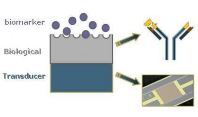
Figure. General concept of a biosensor to detect a target in blood.

New measuring methods using nanoelectronics-based biosensors are of key interest to the pharmaceutical industry because of the variety of applications. They are useful for diagnosis, but also in lab studies (genetic profiling), for preclinical and clinical tests, and for therapy and post therapy. Molecular biosensors detect a biomarker (antibodies, enzymes, DNA, diseased cells, foreign substances such as radioisotopes) in blood. They allow fast, exact and very specific measurement of a biomarker or of several different biomarkers at the same time. Biomarkers are blood substances that are characteristic for a certain biological condition and therefore can be used to determine diseases. A biomarker can be a genetic code within the DNA that is characteristic for a particular disease; but it can also be a diseased cell, such as a cancer cell. Additionally, biomarkers can be foreign substances such as radio isotopes, which are being injected into the blood to examine, for example, organ functions. In order to detect biomarkers in the blood, a blood sample needs to be analyzed. Currently, time-consuming and expensive lab tests have to be carried out in several steps to detect biomarkers. When molecular biosensors are integrated into an electronic system (lab-on-chip), detection can be done much faster and cheaper. Imec develops lab-on-chip systems, such as a breast cancer diagnostic system that can detect cancer cells.

Chip technology’s role in healthcare has the world’s attention. Nanoelectronics will help more patients than we can today, at a lower cost price and for a larger number of diseases, or at least such is the hope. Imec’s research supports the necessary innovation of biomedical instruments for prevention, diagnosis and therapy. Within its life science program, imec cooperates with industrial partners for smart electronic systems in order to study diseases, diagnosis and disease therapy: lab-on-chip systems, nanoparticles for treatment of diseases, technologies for intelligent implants, etc.

Kris Verstreken obtained the degree of Medical Doctor, the Ph.D. degree in Medical Sciences, and the M.S. degree in Electrical Engineering from the Catholic University of Leuven (Belgium). Since 2008, Kris is director of imec’s Life Sciences program.

Hanne Degans received the Ph.D degree in Sciences at the Catholic University of Leuven (Belgium). Since 2008, she works as a scientific editor and external communications officer at imec.

Follow Small Times on Twitter.com by clicking www.twitter.com/smalltimes. Or join our Facebook group
March 8, 2011 — Carbon nanotubes (CNTs) are promising elements for optoelectronic components. However, so far there were no electronic methods to analyze the ultra fast optoelectronic dynamics of the nanotubes. A team of physicists headed by Professor Alexander Holleitner from the Technische Universitaet Muenchen (TUM) has now come up with a new method to directly measure the dynamics of photo-excited electrons in nanoscale photodetectors.

Carbon nanotubes have a multitude of unusual properties which make them promising candidates for optoelectronic components. It has proven extremely difficult to analyze or influence their optic and electronic properties. A team of researchers headed by Professor Alexander Holleitner, a physicist at the Technische Universitaet Muenchen and member of the Cluster of Excellence Nanosystems Munich (NIM), has now succeeded in developing a measurement method allowing a time-based resolution of the so-called photocurrent in photodetectors with picosecond precision.

This new measurement technique is about a hundred times faster than any existing method. It allowed the scientists to measure the precise speed of electrons. In the carbon nanotubes, the electrons only cover a distance of about 8 ten-thousandths of a millimeter or 800nm in one picosecond.

At the heart of the photodetectors in question are carbon tubes with a diameter of about one nanometer spanning a tiny gap between two gold detectors. The physicists measured the speed of the electrons by means of a special time-resolved laser spectroscopy process – the pump-probe technique. It works by exciting electrons in the carbon nanotube by means of a laser pulse and observing the dynamics of the process using a second laser.

The insights and analytic opportunities made possible by the presented technique are relevant to a range of applications, most notably, the further development of optoelectronic components such as nanoscale photodetectors, photo-switches, and solar cells.

The studies were funded by the German Research Foundation (Cluster of Excellence Nanosystems Initiative Munich, NIM) and the Center for NanoScience (CeNS) at Ludwig-Maximilians-Universitaet Muenchen. Further contributions to the publication came from physicists of the University of Regensburg (Germany) and the Swiss Federal Institute of Technology, Zurich.

The experimental results are presented in the journal Nano Letters:
Time-Resolved Picosecond Photocurrents in Contacted Carbon Nanotubes, Leonhard Prechtel, Li Song, Stephan Manus, Dieter Schuh, Werner Wegscheider, Alexander W. Holleitner, Nano Letters 2011, 11 (1), pp 269–272, DOI: 10.1021/nl1036897 http://pubs.acs.org/doi/abs/10.1021/nl1036897

Learn more at www.tum.de

Follow Small Times on Twitter.com by clicking www.twitter.com/smalltimes. Or join our Facebook group
March 8, 2011 – BUSINESS WIRE — TESCAN, scanning electron microscope and focused ion beam workstation maker, delivered a VEGA 3 scanning electron microscope (SEM) to the Massachusetts Institute of Technology (MIT).

The VEGA 3 SEM will support the undergraduate students in the mechanical engineering program, specifically in the Micro and Nano Engineering lab. This course, co-founded by Dr. Sang-Gook Kim encourages creative thinking through hands-on experience via building, observing and manipulating micro and nano scale structures (MEMS, Microfluidics and Nano Materials).

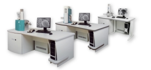
Click to EnlargeThe VEGA 3 includes high-performance electronics for faster image acquisition (down to 20ns/pixel) and signal processing, an ultra-fast scanning system with compensated static and dynamic image aberrations, an extended range of scanning modes using the original Wide Field Optics, In-Flight Beam Tracing for real-time beam optimization, updated software control with high level of automation, and built-in scripting for user-defined applications. The proprietary Intermediate Lens (IML) works as an "aperture changer." The column design, without any mechanical centering elements, allows fully automated column set-up and alignment. Live stereoscopic imaging, using the advanced 3D Beam Technology, enables 3D viewing and navigation of micro- and nanoscale subjects. Jaroslav Klima, CEO of TESCAN, noted that the SEM will perform easily in the leading-edge research arena with multiple users.
TESCAN is focused on research, development and manufacturing of scientific instruments and laboratory equipment. Learn more at www.tescan.com

Follow Small Times on Twitter.com by clicking www.twitter.com/smalltimes. Or join our Facebook group

March 8, 2011 – BUSINESS WIRE — IMT, wafer level packaging (WLP) company and MEMS foundry, introduced its hermetic gold-to-gold (Au-Au) thermo compression bonding. In development for nearly a year, this bond is being actively used in production, and it is said to be one of the lowest cost methods of achieving a hermetic wafer level package bond.

Low-temperate, low-cost wafer bonding could benefit MEMS packaging, as well as other applications.

In addition to the Au-Au thermo compression and the other bond technologies supported, IMT’s flagship remains its proprietary low-temperature hermetic eutectic bond. With sealing temperatures below 190°C and support for reflow temperatures of more than 500°C, this bond is ideal for temperature-sensitive sensors or electronics that require a hermetic package. The bond line width is controlled at less than 50µm.

"More than 80% of our total business makes use of wafer level packaging," said John Foster, IMT Chairman and CEO.

IMT produces and develops MEMS devices and is a pure-play MEMS foundry in the United States. IMT designs, manufactures, tests and supplies products to the RF, biotech, biomed, optical communications, infrared, navigation and general markets servicing Fortune 500 companies as well as startups. For more information, visit http://www.imtmems.com.

Subscribe to Solid State Technology/Advanced Packaging.

Follow Advanced Packaging on Twitter.com by clicking www.twitter.com/advpackaging. Or join our Facebook group

March 7, 2011 — Shipments of complementary metal oxide semiconductor (CMOS) image sensors for digital still cameras (DSCs) are set for rapid growth over the next three years, allowing them to exceed those of charge-coupled devices (CCD) for the first time ever in 2013, according to new IHS iSuppli research. CMOS image sensors are winning over Sony, Canon, and other OEMs with better power consumption, lower fab costs, and circuit integration, among other benefits.

CMOS image sensor shipments for DSCs in 2013 will reach 71.1 million units, up from 30.7 million in 2010. Meanwhile, CCD shipments will decline to 66.9 million in 2013, down from 94.1 million in 2010. By 2014, more than 85 million DSC CMOS units will be shipping, compared to 51 million for CCD.

Figure. Digital still camera (DSC) image sensor unit shipments by technology (millions of units).

"After many years of using CCD technology, original equipment manufacturers (OEM) like Sony, Canon, Kodak, Casio and Samsung now are turning to CMOS, which has narrowed the image quality gap with CCDs to a great degree," said Pamela Tufegdzic, analyst for consumer electronics at IHS. "This has allowed DSC makers to enjoy the advantages provided by CMOS sensors, including lower power consumption and reduced cost."

The lower power consumption of CMOS sensors yields longer battery life. Meanwhile, CMOS sensors are cheaper to produce than CCDs, cutting the cost for manufacturing DSCs. Other advantages of CMOS sensors include their support for multiple channels of sensor data to be read out simultaneously at high speeds, improving the performance of DSCs. CMOS sensors also allow for the possible inclusion of on-chip peripheral circuits, increasing the integration of electronics and reducing the size of DSCs.

Finally, CMOS sensors support backside illumination technology, enabling better quality imaging in low and normal lighting conditions. Backside illumination is especially of interest to camera OEMs that are shifting from CCD technology to CMOS.

Some lingering issues remain, however, involving the switch to CMOS technology. In comparison to CCDs, CMOS image sensors generate more electrical noise, which can result in poor image quality with irregular pixels. CMOS image sensors also create random noise that appears in different pixels at different times, caused by flickering light.

2009 was a tough time for DSCs, as it was for most consumer electronics products. However, IHS believes the worst has passed and that the market is set to expand in 2011 and beyond. Growth will be fueled by lower price points that stimulate demand and drive unit sales. Furthermore, a number of new areas within the DSC market will continue to expand, such as hybrid cameras (video and still images), Wi-Fi digital, and 3D cameras. Such factors, in combination with the positive outlook for digital single-lens reflex (DSLR) cameras, whose prices continue to drop, will increase demand and desire among consumers to use DSCs over their mobile handset cameras in the future.

Read more in "Image Sensors Continue to Experience Demand for 2011 and Beyond," abstract at http://isuppli.com/Abstract/P12201_20110216155231.pdf

IHS iSuppli technology value chain research and advisory services range from electronic component research to device-specific application market forecasts, from teardown analysis to consumer electronics market trends and analysis and from display device and systems research to automotive telematics, navigation and safety systems research. More information is available at www.isuppli.com

Follow Small Times on Twitter.com by clicking www.twitter.com/smalltimes. Or join our Facebook group

March 7, 2011 — Coventor Inc., software supplier for developing micro-electromechanical systems (MEMS), announced availability of SEMulator3D 2011, the latest version of its virtual fabrication software for semiconductor and MEMS process development organizations. It includes the debut of SEMulator3D Reader.

SEMulator3D is already in use by semiconductor companies, MEMS integrated device manufacturers (IDMs), and MEMS foundries for tasks ranging from process integration and documentation of advanced logic and memory process nodes to MEMS design verification.

The SEMulator3D 2011 release provides a three-fold performance boost in model building time and new robust 3D mesh generation capabilities that create silicon-accurate meshes for physics-based simulations used to optimize the performance and manufacturability of semiconductor and MEMS devices. In addition, Coventor is providing the first release of SEMulator3D Reader, a downloadable interactive 3D model viewer that will streamline communications among process development team members and with suppliers and customers.

The release of SEMulator3D 2011 offers 3D virtual fabrication for existing process integration and documentation applications, as well as emerging applications, including novel semiconductor processes, non-destructive metrology, and highly integrated MEMS+CMOS processes.

SEMulator3D’s new mesh generation capability means that device simulations are no longer limited to idealized device models. Surface and volume meshes can be exported to finite element analysis (FEA) and TCAD simulation tools in multiple industry-standard formats, including ans (Ansys), dxf, obj, and unv formats. The meshes are of uniform quality and density suitable for simulation of many physical domains, including mechanical, thermal, and electromagnetics, in addition to coupled physics such as electromechanics.

The new SEMulator3D Reader is a full-featured 3D viewer that uses a compact file format designed for portability. It enables process development and foundry service teams to easily share 3D device models that convey far more information than the static screenshot images or PowerPoint slides typically used to communicate with colleagues or customers. Users are able to interact directly with the models to manipulate the 3D view, see a cross section at any location, toggle visibility of layers, and animate the fabrication process. Comments and annotations can be added for each process step to further streamline communications and documentation throughout the entire development cycle. A downloadable version of the SEMulator3D Reader is immediately available with online access to a variety of sample semiconductor and MEMS 3D models.

"IBM uses Coventor’s SEMulator3D to emulate advanced FEOL, MOL and BEOL integrated processes, with specific attention to 22nm technology and beyond. SEMulator3D allows modeling of a complete process sequence and creates realistic 3D models that can be shared with colleagues. The process/layout editor tools allow development and calibration of a process emulation and expands our understanding of the resulting structures to a variety of layouts," said David Fried, 22nm chief technologist at IBM. "With this capability, our visibility into the full technology implication of process selections and changes has been improved. SEMulator3D has helped IBM predict problems that otherwise would only have been found by subsequent testing and physical failure analysis."

"IMEC uses SEMulator3D for process documentation and design verification. Our SiGeMEMS-above-IC technology allows product developers to monolithically integrate MEMS devices with CMOS circuits, enabling new applications and reduced form factors. By providing SEMulator3D process files with our PDK, we enable designers to verify manufacturability of their designs before tape-out for fabrication. Using SEMulator3D, we can ensure that designers receive the accurate and complete process information they require," commented Stephane Donnay, Ph.D., CMORE program manager at IMEC.

Coventor profiled customer test cases to identify steps that required the most computing time, and then optimized the algorithms and implemented parallel processing support (making use of multi-core CPUs) to achieve performance gains of 3 to 4x over the previous release. SEMulator3D 2011 is more than three times faster for a 25nm flash memory application. In addition, the tool now detects incremental changes to the process description and automatically re-builds only subsequent process steps, saving on average 50% or more in model development time.

"SEMulator3D is our tool…for experimenting with new technologies and ideas," said Thomas Ostermann, staff engineer, Power Technology Development, Automotive Power at Infineon Technologies Austria AG. "We also use SEMulator3D to create 3D cross sections for documentation and training of new colleagues. The ability to generate 3D pictures and animations makes it much easier to explain a process."

Coventor Inc. makes automated design products for micro-electromechanical systems (MEMS) and virtual fabrication of MEMS and semiconductor devices. More information is available at http://www.coventor.com

Follow Small Times on Twitter.com by clicking www.twitter.com/smalltimes. Or join our Facebook group

March 7, 2011 – Marketwire — Boston Micromachines Corporation (BMC), MEMS-based deformable mirror (DM) provider for adaptive optics systems, won a Phase 1 contract for $100,000 from NASA’s Small Business Innovation Research Program (SBIR) to support space-based imaging research.

The Phase 1 project is for the development of a reliable, fault-tolerant microelectromechanical deformable mirror (MEMS-DM) technology, which will fill a critical gap in NASA’s roadmap for future coronagraphic observatories. BMC will implement two innovative, complementary modifications to the MEMS manufacturing process. The team will develop a drive electronics approach that inherently limits actuator electrical current density generated to prevent permanent failure when a short time frame single fault failure occurs, as well as modify the actuator design to mitigate failure due to adhesion between contacting surfaces of the actuator flexure and fixed base.

NASA has identified a current technology need for compact, ultra-precise, multi-thousand actuator DM devices. Space-based telescopes have become indispensible in advancing the frontiers of astrophysics. Over the past decade NASA has pioneered coronagraphic instrument concepts and test beds to provide a foundation for exploring feasibility of coronagraphic approaches to high-contrast imaging and spectroscopy.

"Space-based astronomical imaging systems are inherently challenged by the need to achieve diffraction-limited performance with relatively lightweight optical components. Given the current constraints on fabrication methods, a new manufacturing technique is required to increase reliability and prevent single actuator failures," said Paul Bierden, president and co-founder of Boston Micromachines. "This project will result in innovative advances in component design and fabrication and substantial progress in the development of high-resolution deformable mirrors suitable for space-based operation."

This Phase 1 award is part of NASA’s Small Business Innovation Research programs. The competitive programs afford small businesses the chance to propose unique ideas that meet specific research and development needs of the government. The criteria used to choose these winning proposals include technical merit and feasibility, experience, qualifications, effectiveness of the work plan and commercial potential.

Boston Micromachines Corporation (BMC) makes advanced microelectromechanical systems (MEMS)-based mirror products for use in commercial adaptive optics systems. By applying wavefront correction to produce high resolution images, BMC devices can be used for imaging biological tissue and the human retina and to enhance images blurred by the earth’s atmosphere. The company’s suite of compact deformable mirror (DM) products is cost effective and high performance. For more information on BMC, please visit www.bostonmicromachines.com.

Other NASA news in microelectronics:

Follow Small Times on Twitter.com by clicking www.twitter.com/smalltimes. Or join our Facebook group

March 4, 2011 — A little zinc can do a lot of damage to graphene. Rice University researchers have taken advantage of that to create single-atomic-layer lithography. The Rice lab of chemist James Tour sputtered zinc onto multilayered graphene, enabling the team to remove a single layer at a time without disturbing the layers beneath.

A microscopic checkerboard pattern shows the ability of Rice University’s new technique, as reported in Science, to remove single layers of graphene without disturbing the layers beneath. (Credit: Tour Lab/Rice University)

The discovery could be useful as researchers explore graphene’s electrical properties for new generations of microcircuitry and other graphene-based devices. Graphene, the one-atom-thick form of carbon, won its discoverers the most recent Nobel Prize in physics.

The researchers created a graphene checkerboard by removing horizontal and vertical layers to create a three-dimensional pattern. The researchers were able to create a 100nm line in a sheet of graphene, which suggests the only horizontal limit to the resolution of the process is the resolution of the metal patterning method.

"The next step will be to control the horizontal patterning with similar precision to what we have attained in the vertical dimension," Tour said. "Then there’s no more room at the bottom at any dimension, at least if we call single atoms our endpoint — which it is, for practical purposes."

"The removal of a single sheet of graphene or graphene oxide was a surprise," said Tour, Rice’s T.T. and W.F. Chao Chair in Chemistry as well as a professor of mechanical engineering and materials science and of computer science. "We thought multiple layers would be removed by this protocol, but to see single layers removed is one of those exciting events in science where nature gives us far more than we expected."

The Rice U. researchers printed a micro owl, Rice’s mascot, about 15 millionths of a meter wide. For the owl, Dimiev cut a stencil in PMMA with an electron beam and placed it on graphene oxide. He sputter-coated zinc through the stencil and then washed the zinc away with dilute hydrochloric acid, leaving the embedded owl behind. (Credit: Tour Lab/Rice University)

Tour said the ability to remove single layers of graphene in a controlled manner "affords the most precise level of device-patterning ever known, or ever to be known, where we have single-atom resolution in the vertical dimension. This will forever be the limit of vertical patterning — we have hit the bottom of the scale."

Ayrat Dimiev, a postdoctoral scientist in Tour’s lab, discovered the technique and figured out why graphene is so amenable to patterning. He sputtered zinc onto graphene oxide and other variants created through chemical conversion, chemical vapor deposition (CVD) and micromechanically (the "Scotch-tape" method). Bathing the graphene in dilute hydrochloric acid removed graphene wherever the zinc touched it, leaving the layers underneath intact. The graphene was then rinsed with water and dried in a stream of nitrogen.

Investigation of the sputtered surface before applying the acid wash revealed that the metals formed defects in the graphene, breaking bonds with the surrounding sheet like a cutter through chicken wire. Sputtering zinc, aluminum, gold and copper all produced similar effects, though zinc was best at delivering the desired patterning.

Sputter-coating graphene with aluminum showed similar effects. But when Dimiev tried applying zinc via thermal evaporation, the graphene stayed intact.

Results are reported this week in the journal Science. Read the abstract at: 

A team of Rice University researchers has developed a way to remove layers of graphene from a stack leaving underlying layers in a pristine state. Co-authors of a new Science paper on the research include, from left: Ayrat Dimiev, Alexander Slesarev, Professor James Tour, Zhengzong Sun and Alexander Sinitskii. Missing from the photo is former Rice postdoctoral researcher Dmitry Kosynkin. (Jeff Fitlow/Rice University)

http://www.sciencemag.org/content/331/6021/1168.abstract Co-authors include research associate Dmitry Kosynkin, postdoctoral research associate Alexander Sinitskii and graduate students Alexander Slesarev and Zhengzong Sun, all of Rice.

The Air Force Office of Scientific Research, the Air Force Research Lab through the University Technology Corporation, the Office of Naval Research Graphene MURI Program, and M-I SWACO funded the research.

Video of the researchers discussing their work is available at: http://www.youtube.com/watch?v=RqPg0rebSl8

Follow Small Times on Twitter.com by clicking www.twitter.com/smalltimes. Or join our Facebook group

March 4, 2011 — Researchers in the University of Arizona’s physics department, along with collaborators from the Massachusetts Institute of Technology (MIT) and the National Materials Science Institute in Japan, found that by placing a graphene layer on a material almost identical in structure, boron nitride (BN), instead of the commonly used silicon oxide (SiO2) found in microchips, they could significantly improve its electronic properties.

Click to Enlarge

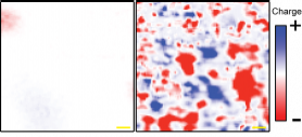
Placed on boron nitride, graphene shows much smaller electric charge fluctuations, shown in red and blue (left) than when mounted on a silicon oxide wafer (right). (Image courtesy of Brian LeRoy/UA)

The study of the physical properties and potential applications of graphene has suffered from a lack of suitable carrier materials that can support a flat graphene layer while not interfering with its electrical properties, the researchers said.

Substituting silicon wafers with boron nitride, a graphene-like structure consisting of boron and nitrogen atoms in place of the carbon atoms, the group was the first to measure the topography and electrical properties of the resulting smooth graphene layer with atomic resolution.

Click to Enlarge

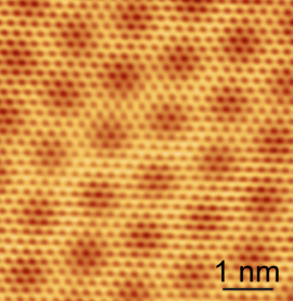
Under the scanning tunneling microscope, graphene reveals its honeycomb structure made up of rings of carbon atom, visible as small hexagons. The larger hexagons result from an interference process occurring between the graphene and the underlying boron nitride. The scale bar measures one nanometer, or one billionth of a meter. (Image courtesy of Brian LeRoy/UA)

"Structurally, boron nitride is basically the same as graphene, but electronically, it’s completely different," said Brian LeRoy, an assistant professor of physics and senior author of the study. "Graphene is a conductor, boron nitride is an insulator."

"We want our graphene to sit on something insulating, because we are interested in studying the properties of the graphene alone. For example, if you want to measure its resistance, and you put it on metal, you’re just going to measure the resistance of the metal because it’s going to conduct better than the graphene."

To measure the topography of the graphene surface, the team uses a scanning tunneling microscope, which has an ultrafine tip that can be moved around. "We move the tip very close to the graphene, until electrons start tunneling to it," Jiamin Xue, a doctoral student in LeRoy’s lab and the paper’s leading author, explained. "That’s how we can see the surface. If there is a bump, the tip moves up a bit."

"Using a scanning tunneling microscope, we can look at atoms and study them," Leroy added. "When we put graphene on silicon oxide and look at the atoms, we see bumps that are about a nanometer in height. Boron nitride…smooths out the bumps by an order of magnitude."

For the spectroscopic measurement, Xue holds the tip at a fixed distance above the sample. He then changes the voltage and measures how much current flows as a function of that voltage and any given point across the sample. This allows him to map out different energy levels across the sample.

"You want as thin an insulator as possible," LeRoy added. "The initial idea was to pick something flat but insulating. Because boron nitride essentially has the same structure as graphene, you can peel it into layers in the same way. Therefore, we use a metal as a base, put a thin layer of boron nitride on it and then graphene on top."

"When you have graphene sitting on silicon oxide, there are trapped electric charges inside the silicon oxide in some places, and these induce some charge in the overlying graphene. You get quite a bit of variation in the density of electrons. If graphene sits on boron nitride, the variation is two orders of magnitude less," LeRoy said.

The team’s results are published in the advance online publication of Nature Materials.

Click to Enlarge

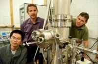
Jiamin Xue, Philippe Jacquod and Brian LeRoy (left to right) with the scanning tunneling microscope they use to study graphene. (Photo by Patrick McArdle/UANews)

In addition to potential applications in integrated circuits, solar cells, miniaturized bio devices and gas molecule sensors, graphene has attracted the attention of physicists for its unique properties in conducting electricity on an atomic level. Graphene has little resistance and allows electrons to behave as massless particles like photons while traveling through the hexagonal grid at very high speeds.

The UA portion of this research was funded by the U.S. Army Research Office and the National Science Foundation.

Follow Small Times on Twitter.com by clicking www.twitter.com/smalltimes. Or join our Facebook group