Tag Archives: Small Times Magazine

March 3, 2011 — Vistec Lithography Inc., electron-beam lithography system supplier, received a major order from Greece. The National Center for Scientific Research (NCSR Demokritos) bought an EBPG5000plusES system for one of its associated Institute of Microelectronics (IMEL). This will be the first 100kV lithography system in Greece, enabling multidisciplinary cutting-edge nano-research.
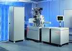
Click to Enlarge"Due to the different fields of research carried out at the IMEL we had very special demands for the new patterning system. It not only had to be capable of a multi user environment but also had to provide high class and efficient nano-lithography in all areas of our activities spanning from nanoelectronic devices to sensors and MEMS/NEMS. The EBPG5000plusES is the perfect match to these requirements and it will allow IMEL to further improve its position at the nanotechnology forefront," said Professor Dimitris Tsoukalas, director of IMEL. The Vistec EBPG5000plusES is a high-performance lithography tool based on reliable and well-proven system architecture. Due to its electron-optical column, the system can expose various substrate types with a spot size down to <2.2nm, enabling nano-dimensional features below 8nm. The system incorporates an interactive graphical user interface (GUI) that provides ease of use for diverse multi user environments.

IMEL is the top research provider of its type in Greece, noted Rainer Schmid, GM at Vistec Lithography, adding that the EBPG5000plusES 100kV system will allow the institute to maintain a leading role in national nano-research, European research projects, networks of excellence, and technology platforms.

NCSR Demokritos is a multidisciplinary Research Center located close to Athens. Its activities are performed in 8 Institutes and are concentrated in the areas of nanosciences & micro-nanotechnology, new materials, energy, health, environment, informatics & telecommunications and cultural heritage.

IMEL is one of the 8 Institutes of NCSR Demokritos with a mission to perform medium- to long-term research in micro and nanotechnology. The Institute supports educational activities in Greece and offers services to external users.

The Vistec Electron Beam Lithography Group is a global manufacturer and supplier of e-beam lithography systems with applications ranging from nano and bio-technology to photonics and industrial environments like mask making or direct writing for fast prototype development and design evaluation.

The Vistec Electron Beam Lithography Group combines Vistec Lithography and Vistec Electron Beam. Vistec Lithography develops, manufactures, and sells electron-beam lithography equipment based on Gaussian Beam technology. Vistec Electron Beam provides electron-beam lithography equipment based on Shaped Beam technology.

Learn more at www.vistec-semi.com

Follow Small Times on Twitter.com by clicking www.twitter.com/smalltimes. Or join our Facebook group

March 3, 2011 – MARKET WIRE — MSGI Technology Solutions Inc. (OTCBB: MSGI), a provider of proprietary solutions to commercial and government organizations, provided a science and technology update to its investors on its lab-on-chip chemical sensing technology being developed for NAsA.

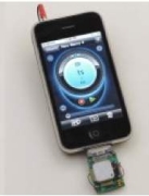
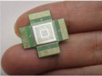
Click to EnlargeAs part of MSGI Space Act Agreements with NASA, a handheld diagnostic device has been developed with medical and environmental testing applications. The new device plugs directly into an iPhone and can collect and analyze chemical data in real time. The device senses chemicals in the air using a sample jet and a multi-channel silicon-based sensing chip with a variety of nanomaterials.

The device consists of 256 nanosensors on the chip and uses a pattern recognition algorithm to identify the ‘finger print’ of the analyte of interest. The sensing device effectively learns the response pattern from changes in resistance correlated to concentration levels of certain target chemicals and gases.

This research has been conducted with support from the US Dept of Homeland Security, US Department of Defense, and MSGI using breakthroughs in nanotechnology and chemical sensing.

Click to EnlargeWithin the medical diagnostic field, the sensor will extract and test breath for a variety of biomarkers indicating various stages of a life-threatening disease. The first such chemical sensor will be used as a non-invasive bloodless test for diabetes. Environmental diagnostic applications include testing the air in a burning building for levels of carbon monoxide and other dangerous or toxic gases, screening for attempts of bio-terrorism.

Jeremy Barbera, CEO of MSGI Technology Solutions, commented, "Alongside our NASA partners, we have been making great technological strides in the areas of chemical sensing and solar energy. Our innovative technology has the ability to improve many facets of society including homeland security, environmental testing, diagnostic testing, energy conservation and much more."

MSGI Technology Solutions Inc. (OTCBB: MSGI) is a provider of proprietary solutions to commercial and government organizations. MSGI has executed several Space Act Agreements with The National Aeronautics and Space Administration (NASA), forming a partnership between MSGI and the NASA Ames Research Center for the purpose of research and development, technology transfer and near-term commercialization of NASA inventions.

Follow Small Times on Twitter.com by clicking www.twitter.com/smalltimes. Or join our Facebook group
March 3, 2011 — Computer scientists at the National Institute of Standards and Technology (NIST) have improved software that can take much of the guesswork out of difficult materials development and environmental simulation problems. 

Click to Enlarge
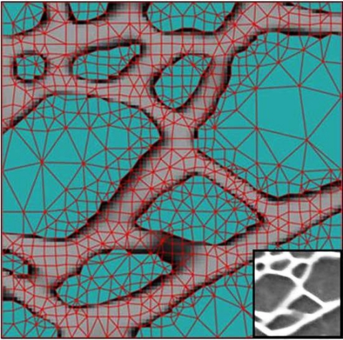
Figure: Once provided with a microscope’s image of a composite material, OOF software can help analyze the effects of the material’s internal structure on stress. Using OOF, researchers can identify the different substances (blue and gray areas) that make up the material and compute their response to stress or other effects, providing clues about how the overall sample will behave. Credit: Langer, NIST

The software package, OOF (Object-Oriented Finite element analysis) is a specialized tool to help materials designers understand how stress and other factors act on a material with a complex internal structure, as is the case with many alloys and ceramics. As its starting point, OOF uses micrograph images of a material taken by a microscope. At the simplest level, OOF is designed to answer questions like, “I know what this material looks like and what it’s made of, but I wonder what would happen if I pull on it in different ways?” or “I have a picture of this stuff and I know that different parts expand more than others as temperature increases; I wonder where the stresses are greatest?”

OOF has been available in previous versions since 1998. The new version (2.1) adds a number of improvements:

  • improves OOF’s ability to envision non-linear behavior, such as large-scale deformation, which plays a significant role in many types of stress response;
  • allows users to analyze a material’s performance over time, not just under static conditions as was the case previously;
  • templates allow programmers to plug in their own details and formulas describing a particular substance.

Later this year, the team expects to enable users to analyze three-dimensional micrographs of a material, rather than the 2D "slices" that can be analyzed at this point.

OOF is available for free download at http://www.ctcms.nist.gov/oof/oof2/. The package runs on Unix like systems, including Linux, OS X and Linux-like environments within Windows.

The National Institute of Standards and Technology (NIST) is an agency of the U.S. Commerce Department.

Follow Small Times on Twitter.com by clicking www.twitter.com/smalltimes. Or join our Facebook group

March 3, 2011 – BUSINESS WIRE — Excelitas Technologies, optoelectronics provider, achieved record, world-class performance results for high photon detection efficiency (PDE) and low dark counts in the development and commercialization of its solid state silicon photomultipliers (SiPM) technology. SiPMs are an important element in Excelitas’ low light level detection (L3D) suite of technologies and products targeting the medical and analytical market space.

The results have been published and presented at the "CERN Industry-Academia Matching Event on SiPM and Related Technologies," in Geneva, Switzerland in February. The event brought together 120 experts active in cutting-edge photon detection work from both industry and academia.

In 2009, the company entered into an exclusive agreement with Max Planck Innovation, the technology transfer organization of the Max Planck Society, for the licensing of its ultra-fast, low cross-talk SiPM technology. Silicon photomultipliers offer very high PDE, ultra-short response time, and low power consumption, suiting low-light level applications such as fluorescence and molecular imaging in life sciences, clinical diagnostics, and analytical instrument sectors.

Excelitas Technologies is showcasing its broad array of light emission and low light level detection solutions tailored specifically for the analytical and life sciences markets at Pittcon 2011, Booth 5060. Pittcon 2011 takes place March 13-18 at the Georgia World Congress Center in Atlanta, GA.

Excelitas Technologies targets illumination, detection and other high-performance technology needs of OEM customers. The company was previously the Illumination and Detection Solutions (IDS) business unit of PerkinElmer, and is now owned by Veritas Capital. Learn more at www.excelitas.com

Follow Small Times on Twitter.com by clicking www.twitter.com/smalltimes. Or join our Facebook group

March 2, 2011 – A two-day seminar later this month in San Jose will offer insights into testing of MEMS inertial sensors, and seek to develop a "strategic plan" to decrease cost and increase efficiency of MEMS device testing.

The two-day MEMS Testing Standards Workshop and M2M Forum, hosted by the MEMS Industry Group (MIG) on March 16-17, will first offer a testing standards workshop, looking at current practices, needs, and opportunities for qualifying and testing inertial sensors. Speakers include Analog Devices, Acutronic, MEMSCAP, and NIST. Keynoting an evening reception will be Gary O’Brien, director of corporate research in Robert Bosch’s advanced MEMS design group, reviewing the company’s MEMS fabrication techniques and the importance of test procedures.

The second day will encompass a "M2M Forum" (née MEMS Technology Roadmap and Industry Congress, or METRIC), with the goal of laying out an industry plan for reducing cost of MEMS devices through testing strategies. Working groups will focus on system-level testing (moderated by TI and Silex Microsystems), innovations in testing (moderated by Acuity and AM Fitzgerald), and MEMS testing protocols and standards (moderated by NIST and the Science Technology Policy Institute).

The event is being held March 16-17 at the Doubletree San Jose hotel. Go to the MEMS Industry Group’s Web site for information on registering. And take the MIG’s (anonymous) survey on what MEMS standards are in use at your company or organization.

March 2, 2011 — Researchers at North Carolina State University have developed a cheap and easy method for assembling nanowires, controlling their alignment and density. Dr. Yong Zhu, an assistant professor of mechanical and aerospace engineering at NC State, deposited the nanowires on a stretched rubber substrate, then released the tension on the substrate. When the nanowires settled, they aligned at a right angle to where the tension originated.

The researchers hope the findings will foster additional research into a range of device applications using nanowires, from nanoelectronics to nanosensors, especially on unconventional substrates such as rubber, plastic and paper.

"Alignment is a critical first step for developing devices that use nanowires," says Zhu, who co-authored a paper describing the research. "Hopefully our simple and cost-effective method will facilitate research in this field."

Aligning nanowires is challenging because they are created as a profusion of randomly oriented nanoscale wires between 10 and 100nm in diameter. Before any practical applications can be pursued, the user must assemble the nanowires in an orderly way. Specifically, users need to align the nanowires in a common direction and define their density. Controlling alignment and density is commonly called "assembling" the nanowires.

The more the rubber substrate is stretched, the more aligned the nanowires will be, and the greater the nanowire density will be. "Our method is cost-effective," says Feng Xu, a Ph.D. student working on this project. "It can also be used for nanowires synthesized by different methods or processed in different conditions, for instance, silver nanowires synthesized in solution and silicon nanowires synthesized by the vapor-liquid-solid method, as demonstrated in our work."

Previous research has presented a number of other methods for assembling nanowires. The new method can be used in conjunction with previous methods to achieve even better nanowire assembly.

The use of a rubber substrate in this method facilitates broad research and manufacturing sectors. For example, a key element of research into stretchable nanoelectronics involves aligning nanowires on a stretchable rubber substrate. Similarly, rubber is also the material used as stamps in transfer printing, a fabrication method used in manufacturing nanodevices on diverse substrates ranging from silicon to glass to plastic.

Zhu notes that the initial step of the method, when the nanowires are first deposited on stretched rubber, sometimes yields an inconsistent degree of nanowire alignment. The team is currently working to understand the fundamental interface mechanics, including adhesion and static friction, between nanowires and rubber substrates, which is expected to lead to a better control of the assembly process and hence a higher yield of the nanowire assembly.

The paper, "Strain-Release Assembly of Nanowires on Stretchable Substrates," was published Feb. 22 in ACS Nano. The paper was co-authored by Zhu, Xu, NC State Ph.D. student John Durham, and Dr. Benjamin Wiley, an assistant professor at Duke University. Access it online here: http://pubs.acs.org/doi/abs/10.1021/nn103183d
Abstract: A simple yet effective method for assembly of highly aligned nanowires (NWs) on stretchable substrates is reported. In this method, NWs were first transferred to a strained stretchable substrate. After the strain was released, the NWs aligned in the transverse direction and the area coverage of the NWs on the substrate increased. This method can be applied to any NWs deposited on a stretchable film and can be repeated multiple times to increase the alignment and density of the NWs. For silver (Ag) and silicon (Si) NWs on poly(dimethylsiloxane) (PDMS) substrates, the probability of NW alignment increased from 29% to 90% for Ag NWs, and from 25% to 88% for Si NWs after two assembly steps; the density increased by 60% and 75% for the Ag and Si NWs, respectively. The large-strain elasticity of the substrate and the static friction between the NWs and the substrate play key roles in this assembly method. We find that a model that takes into account the volume incompressibility of PDMS reliably predicts the degree of NW alignment and NW density. The utility of this assembly method was demonstrated by fabricating a strain sensor array composed of aligned Si NWs on a PDMS substrate, with a device yield of 95%.

The research was funded by the National Science Foundation.

NC State’s Department of Mechanical and Aerospace Engineering is part of the university’s College of Engineering.

Follow Small Times on Twitter.com by clicking www.twitter.com/smalltimes. Or join our Facebook group

March 1, 2011 — Electrical energy can be generated from a temperature difference in a circuit with suitable materials. In simulations, ETH Zurich scientists show which materials are most likely to succeed in a thermoelectric process.

Click to Enlarge 
 
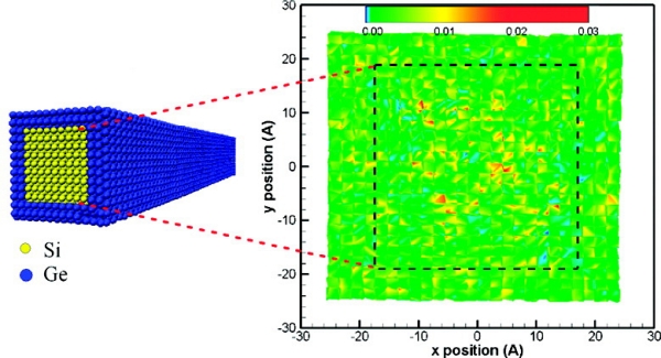
The computer-simulated thermoelectric material is an atomically thin germanium (Ge) coating on a thin silicon nanowire, which dramatically reduces the wire’s thermal conductivity. Only the red spots in the cross-section indicate high heat flux areas. The nanowires look like long french fries: elongated rectangular cuboids more than 300 silicon unit cells long and with a cross-section 9 unit cells wide and 9 high. The wires are 160nm long and about 5nm in equivalent diameter. The nanowires are coated with an atomically-thin layer of germanium, the thickness of the layer being only one to two unit cells of the semiconductor material.

A SiGe nanowire with this construction would be a worthy candidate for use in thermoelectricity. The only problem is that, up to now, the tiny semiconductor wire in this form exists only in the computer of Ming Hu, a post-doctoral scientist in the group of Dimos Poulikakos, Professor of Thermodynamics at the Institute of Energy Technology. Professor K. Giapis of the California Institute of Technology, USA, who spent his Sabbatical leave with the Poulikakos group at ETH Zurich, also collaborated in performing the research that led to the development of this wire.

Thermoelectricity exploits the fact that temperature and electricity can be under certain conditions inter-convertible. Due to the Seebeck effect, a small electrical voltage occurs in a circuit when a temperature difference is present between the contact points of two different kinds of electrical conductors in the circuit. However, not all conducting or semiconducting materials are suitable for thermoelectricity generation. To exhibit high conversion coefficients rendering a material viable to realistic applications the material thermal conductivity must be as small as possible, whereas its electrical conductivity must be large. Dimos Poulikakos says, "Such materials are practically non-existent in nature."

Although the thermal conductivity of bulk silicon is high, this thermal conductivity deteriorates as soon as the semiconductor is converted into a wire-like nanostructure. "Even pure silicon nanowires are not good enough for efficient energy conversion," says Ming Hu.

Through computer simulations, Hu Ming has showed that silicon nanowires conduct heat even more poorly if they are coated with an atomically thin layer of germanium, another semiconductor. The thermal conductivity decreases by 75% compared to pure silicon nanowires, and does so at room temperature. When Hu added more layers of germanium in his model, the thermal conductivity increased again.

The researchers showed that the reason for the dramatic reduction in the thermal conductivity of germanium-coated silicon nanowires lies in the altered vibration modes of the phonons that transport heat through the crystal lattice. The wavelengths of the particles were shortened and compressed at the interfacial layer between the silicon and the germanium, which blocked the heat transport to a very large degree.

Therefore, the researchers conclude that thin silicon nanowires should be coated with one or two layers of germanium to enable a significant step toward achieving viable thermoelectric processes.

The SiGe nanowires still exist only in Ming Hu’s computer. However, the plan is to manufacture them soon in Poulikakos’ laboratory for real experiments. Thermoelectric methods could make an important contribution to alternative energy production in the future. For example, the ETH Zurich professor can envisage that, with the aid of suitable installations, they could be used to exploit the waste heat from machines or buildings to generate electricity, which can be stored or fed into the grid. Based on the present state of knowledge, one could imagine devices that supply electricity to individual houses or portable equipment. Thermoelectric modules, e.g. as big as a kitchen table, could also act as solar panels to generate electrical energy from solar energy. Poulikakos warns that "such practical applications are still a rather long way into the future."

Reference

Hu M, Giapis KP, Goicochea JV, Zhang X and Poulikakos D., Significant Reduction of Thermal Conductivity in Si/Ge Core-Shell Nanowires., Nano Letters, 2011, 11, 618–623. doi: 10.1021/nl103718a

Follow Small Times on Twitter.com by clicking www.twitter.com/smalltimes. Or join our Facebook group

March 1, 2011 – Business Wire — CVD Equipment Corporation (NASDAQ: CVV) and Graphene Laboratories Inc. now offer commercial CVDGraphene research starter materials and customization services for transparent and conductive CVD-grown graphene films, transferred onto substrates such as insulating silicon dioxide, plastic, and glass.

These materials and services target accelerated development of novel graphene-enabled products that are compatible with standard semiconductor processing. CVD Equipment Corporation manufactures CVD-grown graphene materials in its Application Laboratory. The transfer of Graphene onto a variety of standard and customer-supplied substrates is performed jointly with Graphene Laboratories Inc., which directly markets the products and services worldwide using CVD Equipment Corporation’s CVDGraphene trademark.

Since our first commercial offering of 2D CVDGraphene materials in Q2 2010, our CVDGraphene material has been supplied to several hundred researchers worldwide. Interest in graphene materials was further enhanced by the awarding of the Nobel Prize in Physics in October 2010 for the discovery and isolation of graphene. By offering a Graphene transfer service onto customer-specified materials, we will fulfill strong demand by academic and industrial researchers, said the companies’ representatives. CVD-grown graphene yields high-quality large-scale graphene coatings, stated Dr. Elena Polyakova, president and CEO of Graphene Laboratories, Inc. "In addition to offering off-the-shelf products, we also offer contract process development and customized Graphene products," Polyakova added.

This transfer service will enable better customer support for graphene incorporation into electronic, solar, bio and medical fields. Single-layer graphene films on an insulator like silicon dioxide are a starting material for developing graphene-based transistors, NEMS and MEMS, and sensors. Transparent graphene films on glass and plastics are of interest to developers of touch-screen displays, flexible electronics, and solar cells, says Karlheinz Strobl, VP of business development for CVD Equipment Corporation.

Graphene Laboratories Inc. brings functional graphene materials and devices to market. For further information about Graphene Laboratories Inc., visit www.graphenelab.com

CVD Equipment Corporation (NASDAQ: CVV) is a designer and manufacturer of standard and custom state-of-the-art equipment used in the development, design and manufacture of advanced electronic components, materials and coatings for research and industrial applications. Learn more at www.CVDequipment.com

Follow Small Times on Twitter.com by clicking www.twitter.com/smalltimes. Or join our Facebook group

March 1, 2011 — A team led by Jan Schroers, a materials scientist at Yale University, has shown that some recently developed bulk metallic glasses (BMGs) — metal alloys that have randomly arranged atoms as opposed to the orderly, crystalline structure found in ordinary metals — can be blow molded like plastics into complex shapes that can’t be achieved using regular metal, yet without sacrificing the strength or durability that metal affords. The material is able to take on a seemingly endless variety of forms.

Click to Enlarge

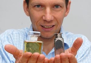
Jan Schroers and his team have developed novel metal alloys that can be blow molded into virtually any shape.

"These alloys look like ordinary metal but can be blow molded just as cheaply and as easily as plastic," Schroers said. So far the team has created a number of complex shapes, including seamless metallic bottles, watch cases, miniature resonators, and biomedical implants. These shapes can be molded in less than a minute and are twice as strong as typical steel.

The materials cost about the same as high-end steel, Schroers said, but can be processed as cheaply as plastic. The alloys are made up of different metals, including zirconium, nickel, titanium and copper.

The team blow molded the alloys at low temperatures and low pressures, where the bulk metallic glass softens dramatically and flows as easily as plastic but without crystallizing like regular metal. It’s the low temperatures and low pressures that allowed the team to shape the BMGs with ease, versatility and precision, Schroers said. To carefully control and maintain the ideal temperature for blow molding, the team shaped the BMGs in a vacuum or in fluid.

"The trick is to avoid friction typically present in other forming techniques," Schroers said. "Blow molding completely eliminates friction, allowing us to create any number of complicated shapes, down to the nanoscale."

Schroers and his team are using their new processing technique to fabricate miniature resonators for microelectromechanical systems (MEMS) as well as gyroscopes and other resonator applications.

In addition, by blow molding the BMGs, the team was able to combine three separate steps in traditional metal processing (shaping, joining and finishing) into one, allowing them to carry out previously cumbersome, time- and energy-intensive processing in less than a minute.

"This could enable a whole new paradigm for shaping metals," Schroers said. "The superior properties of BMGs relative to plastics and typical metals, combined with the ease, economy and precision of blow molding, have the potential to impact society just as much as the development of synthetic plastics and their associated processing methods have in the last century."

Their findings are described online in the current issue of the journal Materials Today. Other authors of the paper include Thomas M. Hodges and Golden Kumar (Yale University); Hari Raman and A.J. Barnes (SuperformUSA); and Quoc Pham and Theodore A. Waniuk (Liquidmetal Technologies).

Learn more at www.yale.edu.

Follow Small Times on Twitter.com by clicking www.twitter.com/smalltimes. Or join our Facebook group

By Debra Vogler, senior technical editor

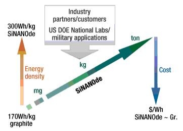
March 1, 2011 – Nanosys’ process-ready silicon composites (SiNANOde, Fig 1.) increase lithium ion (Li-ion) battery cell capacity without compromising cycle life. Yimin Zhu, director, battery & fuel cell, at Nanosys, recently spoke at the IEEE Bay Area Nanotechnology Council lunch forum (2/15/11, Santa Clara, CA).

Click to Enlarge
Figure 1. SiNANOde system. SOURCE: Nanosys

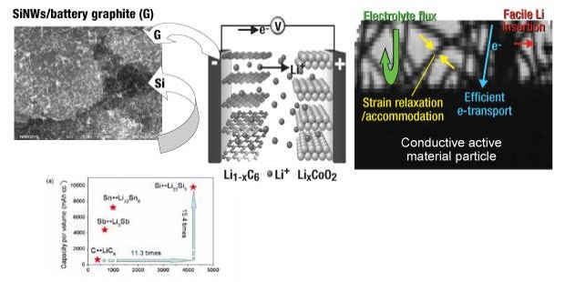
The SiNANOde nanomaterial deforms to fill void areas in the carbon anode material matrix and remains intact and fully functional after 100% DoD cycle testing. The technology also demonstrated a >2× capacity improvement using 10% additive in a Li+ battery anode. Nanosys is co-developing battery solutions with several of the world’s largest Li+ battery makers, noted Zhu. And volume revenue shipments are expected in 2011. Figure 2 shows the current status of the technology.

Click to Enlarge
Figure 2. SiNANOde technology status. SOURCE: Nanosys

In his presentation, Zhu noted how the value in the nanotechnology materials revolution is shifting to novel, tunable materials. “Architected materials not only can be processed using the mature means, but also allow the control of microstructure resulting in unique products,” said Zhu.

Click to EnlargeListen to Zhu’s interview: Download (iPhone/iPod users) or Play Now

In a podcast interview at the event, Zhu discusses details on how silicon nanocomposites are being used to accelerate the improvement in storage capacity of Li-ion cells with Debra Vogler, senior technical editor. He outlined how Nanosys was able to overcome some of the challenges in developing the microstructure of its architected materials for energy storage solutions. One of the capabilities the company developed was a new prototyping process, the goal of which was to develop a substrate-free growth process; Zhu describes the process.

Listen to another interview with Nanosys, this one about quantum dots, here.

Follow Small Times on Twitter.com by clicking www.twitter.com/smalltimes. Or join our Facebook group