Tag Archives: Small Times Magazine

February 23, 2011 — No two quantum dots are identical, but a new etching method for shaping and positioning these semiconductor nanocrystals might change that. Tests at the National Institute of Standards and Technology (NIST) also confirm that etched quantum dots emit single particles of light (photons), boosting prospects for powering new types of devices for quantum communications.
 

Click to Enlarge
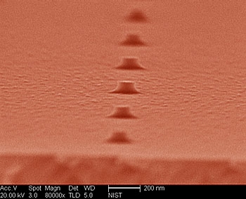
Image. Colorized micrograph of quantum dots made using electron beam lithography and etching. This type of quantum dot can be shaped and positioned more reliably than dots made with conventional crystal growth methods. Credit: Verma/NIST

The conventional way to build quantum dots is to grow them like crystals in a solution, but this somewhat haphazard process results in irregular shapes. The new, more precise process was developed by NIST postdoctoral researcher Varun Verma when he was a student at the University of Illinois. Verma uses electron beam lithography (e-beam litho) and etching to carve quantum dots inside a semiconductor sandwich (quantum well) that confines particles in two dimensions. Lithography controls the dot’s size and position, while sandwich thickness and composition — as well as dot size — can be used to tune the color of the quantum dot’s light emissions.

Some quantum dots are capable of emitting individual, isolated photons on demand, a crucial trait for quantum information systems that encode information by manipulating single photons. In new work reported in Optics Express,* NIST tests demonstrated that the lithographed and etched quantum dots work as sources of single photons. The tests were performed on dots made of indium gallium arsenide (InGaAs). Dots of various diameters were patterned in specific positions in square arrays. Using a laser to excite individual dots and a photon detector to analyze emissions, NIST researchers found that dots 35 nanometers (nm) wide, for instance, emitted nearly all light at a wavelength of 888.6 nm. The timing pattern indicated that the light was emitted as a train of single photons. 

NIST researchers now plan to construct reflective cavities around individual etched dots to guide their light emissions. If each dot can emit most photons perpendicular to the chip surface, more light can be collected to make a more efficient single photon source. Vertical emission has been demonstrated with crystal-grown quantum dots, but these dots can’t be positioned or distributed reliably in cavities. Etched dots offer precise positioning and the possibility of making identical dots, which could be used to generate special states of light such as two or more photons that are entangled, a quantum phenomenon that links their properties even at a distance.

The quantum dots tested in the experiments were made at NIST. A final step was carried out at the University of Illinois, where a crystal layer was grown over the dots to form clean interfaces.

* V.B. Verma, M.J. Stevens, K.L. Silverman, N.L. Dias, A. Garg, J.J. Coleman and R.P. Mirin. Photon antibunching from a single lithographically defined InGaAs/GaAs quantum dot. Optics Express. Vol. 19, No. 5, Feb. 28,  2011, p. 4182. Posted online Feb. 17, 2011. Read the abstract here.

The National Institute of Standards and Technology (NIST) is an agency of the U.S. Commerce Department.

Follow Small Times on Twitter.com by clicking www.twitter.com/smalltimes. Or join our Facebook group
February 23, 2011 — Nitto Denko Asia Technical Centre (NAT) will be expanding its Singapore base to include a prototyping centre in Singapore. The center will be pioneered at Singapore’s Agency for Science, Technology and Research (A*STAR) Institute of Materials Research and Engineering (IMRE) under a unique Lab-in-RI* program. NAT can leverage on existing infrastructure, research expertise, and save cost on facilities and equipment while working to establish the new prototyping center.
 
The decision for the new center stems from IMRE’s successful R&D project with NAT on optical waveguide devices, which are cheaper to manufacture and more sensitive than current alternatives. NAT now wants to explore the biosensing applications of these devices and put them into a new range of low-cost, easy-to-use, home-based, consumer biosensors.
 
"The optical waveguide devices that were developed will give us the opportunity to create version 2.0 biosensors for future homes," said Dr Su Xiaodi, a senior scientist who heads the IMRE research team. She will be working with NAT to put the devices into home-based biosensors that allow users to monitor their health with greater frequency and care, in their home, between visits to the doctor. The targeted users are those with health conditions that could change rapidly or require immediate attention.
 
"IMRE has been a credible partner since our initial collaboration in 2008, and we would like to continue to draw on IMRE’s intellectual resources and excellent facilities to further our R&D activities in Singapore," said Dr Visit Thaveeprungsriporn, Director of NAT.
 
"The new sensor demonstrates how materials science research can benefit even the biomedical industry," said Prof Andy Hor, IMRE’s executive director, adding that the prototyping lab in IMRE shows how industrially relevant research institutes can be.
 
Nitto Denko is one of Japan’s leading diversified materials manufacturer and a major producer of optical films used in LCD TVs. It invested S$10 million in setting up the Nitto Denko Asia Technical Centre (NAT) in Singapore to work on organic electronics research in 2008.
 
The IMRE-Nitto Denko team will begin R&D development at the new prototyping center this month, with a prototype expected to be available in early 2012.

IMRE has built strong capabilities in materials analysis, characterization, materials growth, patterning, fabrication, synthesis and integration. State-of-the-art facilities include the SERC Nanofabrication and Characterisation Facility to conduct world-class materials science research. Industry-coupled research is conducted on organic solar cells, nanocomposites, flexible organic light-emitting diodes (OLEDs), solid-state lighting, nanoimprinting, microfluidics and next generation atomic scale interconnect technology. For more information about IMRE, please visit www.imre.a-star.edu.sg

The Agency for Science, Technology and Research (A*STAR) is the lead agency for fostering world-class scientific research and talent for a vibrant knowledge-based and innovation-driven Singapore. A*STAR oversees 14 biomedical sciences, and physical sciences and engineering research institutes, and seven consortia & centres, which are located in Biopolis and Fusionopolis, as well as their immediate vicinity. For more information about A*STAR, please visit www.a-star.edu.sg.

Nitto Denko Asia Technical Centre Pte Ltd manages the Integrated Organic Optoelectronic Sensing Device Project – three concurrent research projects with the Data Storage Institute, Institute of Materials Research & Engineering and Nanyang Technological University, to advance the field of organic electronic device development.

*Lab-in-RI – A laboratory based in one of A*STAR’s research institutes (RIs) in which the RIs provide partners with infrastructure and framework at an early stage of their R&D projects, allowing companies to jumpstart their R&D activities in Singapore.

Follow Small Times on Twitter.com by clicking www.twitter.com/smalltimes. Or join our Facebook group

February 22, 2011 – Vocus/PRWEB — GIA released a global report, "Micro Electromechanical Systems (MEMs) Devices: A Global Strategic Business Report," on the micro electromechanical system (MEMS) devices market, which is forecast to reach US$9.2 billion by 2015. An uptick in passenger car production, improving consumer demand, and dwindling stockpiles in the supply chain have revived MEMS shipments. Investments in new product development, innovation, and expansion of production capacity bode well for the future of the market.

The prolonged recession and credit crisis triggered price, volume, and revenue volatility in the MEMS industry. Consumer demand weakened for electronic devices/equipment, home appliances, telecommunications equipment, and automobiles. Demand for MEMS devices witnessed marked declines in the automotive and consumer products end-use sectors.

The automobile industry, a major high-volume end-user of MEMS technologies, was the worst affected by the recession. Although shielded to a degree by mandatory regulatory safety standards, especially in Europe and North America, automotive MEMS applications witnessed weakened business prospects as a result of the crushing effect of depressed automotive production. Investments in high-end dashboard electronics waned. Cheaper, affordable, less-equipped models additionally lowered demand for accelerometers for use in airbags, tire pressure monitoring systems (TPMS), and vehicle stability control.

Following automotive applications, the consumer MEMS sensor segment was worst hit. Specific segments such as mobile phones, PDAs, and business projectors fell hardest.

The recession also made a disproportionate impact on industrial production as a result of reduced manufacturing, commercial, and economic activity, thereby hurting industrial applications of MEMS for oil/gas exploration, instrumentation, and process industries, such as, food & beverage, chemicals, pharmaceuticals, plastics, rubber, textiles, among others.

In the telecommunication space, MEMS applications in optical networks also softened significantly. Network operators had to prune down investment outlays in 2008 and 2009 to hedge the financial weakness in the market as well as in the balance sheets. Cooling demand for fiber optic communication services, and broadband Internet services frustrated telecom carriers and as a result pushed fiber optic networking projects into an uncertain and unstable period. Several fiber optic broadband projects have been delayed as a result of network operators reining in capital investments. All of these factors impacted demand for optical telecom network equipment, and in the process the market for optical MEMS in telecom equipment.

Additionally, the complete meltdown of the real estate, housing and construction industry resulted in major disruptions of fiber to green field projects. Cancellation of new building projects resulted in reduced demand for fiber to the home (FTTH) technologies. Also impacted were fiber optics in brown field projects. All of these factors indirectly resulted in bringing down the level of orders for optical MEMS used in metro and long-haul optical telecommunications gear. Use of optical telecom MEMS in 1XN switches, Variable Optical Attenuators (VOAs), cross connects, Wavelength-Selective Switching Reconfigurable Optical Add/Drop Multiplexers (WSS ROADMs) and tunable filters, therefore withered, although temporarily.

With the recession now at its tail end, a sanguine future awaits the world MEMS market, with MEMS device manufacturers focusing on research and development to break into newer application areas. Microsensors and microactuators, which represent the hallmark of the electromechanical domain, are finding use in countless applications. Integrators will be reinforcing their MEMS component stocks to develop new state-of-the-art products, which deliver key features and functionality involving MEMS technology. Although commoditization has already set in with high-volume applications like consumer electronics and automotives, the technology continues to witness radical changes in other sectors like industrial, healthcare, and semiconductor, wherein MEMS+IC are influencing the traditional architecture of System on Chip (SoC).

MEMS technology to make medical diagnostic and monitoring technologies less invasive will garner special attention, especially so against a backdrop of a rapidly aging world population. The value proposition revolving around patient comfort, ease of drug delivery, and ensuing patient compliance will drive demand for MEMS in this space.

Inkjet printheads is the largest selling MEMS device. However, the inkjet printheads market is suffering the two-fold impact of the global recession and the ongoing transition from disposable to permanent printheads. As a result, unit shipments are forecast to decline through 2015. Beginning from 2011, MEMS displays will see encouraging growth due to demand for pico projectors and new MEMS flat-panel technologies for consumer electronics. ESC mandates will help spur the sales of accelerometers, gyroscopes, and high-pressure sensors, whereas TPMS mandates will propel MEMS pressure sensor sales by 2015. Europe and US account for a major share of the global Micro Electromechanical Systems (MEMs) Devices revenues, as stated by the new market research report. Global demand for MEMS in Medical/BioMedical End-Use is expected to increase at a robust pace during 2007 through 2015 period.

Major players in the marketplace include Analog Devices Inc., Apogee Technology Inc., Bosch Sensortec, Colibrys Ltd, Coventor Inc., Dalsa Semiconductor, Epson Toyocom, Hewlett-Packard, Invensense, IntelliSense Software Corporation, Kavlico Corporation, Kistler Instrument Corp., LioniX BV, MEMSCAP S.A., Memsic Inc., Micralyne Inc., NeoPhotonics Corporation, Panasonic Corp, Sensonor Technologies, Silicon Microstructures, Inc., STMicroelectronics, TowerJazz, Texas Instruments Inc, among others.

The research report titled “Micro Electromechanical Systems (MEMs) Devices: A Global Strategic Business Report” announced by Global Industry Analysts, Inc., provides a comprehensive review of market trends, issues, drivers, company profiles, mergers, acquisitions and other strategic industry activities. The report provides market estimates and projections (in US$) for major geographic markets including the United States, Canada, Japan, Europe (France, Germany, Italy, UK, Spain, Russia, Rest of Europe), Asia-Pacific, Latin America and Rest of World. End Use segments analyzed include Commercial/Industrial, Medical/BioMedical, Telecommunication, Computers, and Other Applications. Global MEMS devices market is also analyzed by product categories, such as, Accelerometers, Gyroscopes, Inkjet heads, Wafer Probes & Optical MEMS, Pressure Sensors, and Others. For more details, visit
http://www.strategyr.com/Micro_Electromechanical_Systems_MEMs_Devices_Market_Report.asp

Follow Small Times on Twitter.com by clicking www.twitter.com/smalltimes. Or join our Facebook group
 

Update, February 22: MEMStim received $27,000 for best business and presentation, and outstanding team.

MEMStim sells MEMS electrode leads to medical device companies and won $20,000 for the Pryor-Hale award for best business, $5,000 for the Williamson award for Outstanding Business and Business/Engineering Team and won $2,000 for the Outstanding Presentation Award.

MEMStim plans to sell MEMS electrode leads to medical device companies for integration into their targeted nerve stimulation devices. Ultimately, the company is committed to improving the standard of patient care in neurostimulation. The two MBA students and Doctorate student that form the company team will use the award money to quantify regulatory risks and further prototype development.

"The Michigan Business Challenge Best Business Award is an incredible honor because of the caliber of the judges and other businesses in the competition," said Angelique Johnson, 2011 EECS M.S./Ph.D. and member of the MEMStim team. "We are a strong team and have learned new entrepreneurial skills throughout the competition that build upon our diverse past experiences and will help us bring our technology to market." 


February 8, 2011 – PRNewswire-USNewswire — The Samuel Zell & Robert H. Lurie Institute for Entrepreneurial Studies at the University of Michigan Ross School of Business announced that eight teams have advanced to the semi-finals of this year’s Michigan Business Challenge, including MEMStim, an ODM that sells MEMS electrode leads for medical devices.

The multi-round business plan competition is a cornerstone of the Institute’s action-based educational programming, which enables students to put their entrepreneurial passions into practice while studying and provides them the resources necessary to transform promising business ideas into successful ventures.

Now in its 28th year, The Michigan Business Challenge has evolved from a one-day competition to encourage entrepreneurship and business development among students into a four-month event that exposes students across the University to the rigorous business development and planning process required to commercialize a great idea. Nearly half of the competing teams include students from Engineering, Medicine, Law, and other areas of study, and all teams are provided with training and invaluable feedback at each phase from judges, which include seasoned business leaders and professional leaders.

"In the past decade alone, the Michigan Business Challenge has engaged over 500 teams, many of which have gone on to grow into successful ventures here in Michigan and far beyond," said Tom Kinnear, Executive Director of the Samuel Zell & Robert H. Lurie Institute for Entrepreneurial Studies. "Many students come here eager to bring their own business ideas to fruition, leveraging coursework and programs such as this one to fine-tune plans, develop go-to-market strategies and establish important relationships. It is the opportunities created by this action-based education that sets the Institute apart from other entrepreneurial programs out there."

The 2011 semi-finalist teams represent sectors including medicine, life sciences, high technology and web services. They are:

  • Brio Device – a medical device company whose flagship product, SmartAirway, is designed to improve the success of emergency intubations.
  • IRIZ Technologies – a company that looks to revolutionize cancer treatment by producing and selling micro-fluidic assays (drug-testing environments) to research organizations and pharmaceutical companies.
  • MEMStim – an original design manufacturer selling MEMS electrode leads to medical device companies for integration into their targeted nerve stimulation devices.
  • ReGenerate – a company that designs, markets and leases on-site anaerobic digesters to food service operators to transform unwanted and costly organic waste into a renewable source of energy and nutrient-rich compost.
  • Reveal Design Automation – a technology provider that solves the chip verification scalability challenge, enabling chip design firms to eliminate more bugs in more complex designs with less time and with fewer people.
  • STIgma Free – a point-of-care medical diagnostics firm focused initially on the rapid diagnosis of sexually transmitted infections (STIs). 
  • SurveyBroker – a website that will match businesses and consultancies with survey fieldwork companies that can best meet their market research needs.
  • Thoosa – an international freight brokerage specializing in container shipments that identifies the best shipping options in terms of ocean carrier availability, cost, service level, and carbon production rates.

Many teams go on to participate in national intercollegiate competitions, where they often earn enough seed funding to fuel the initial stages of business growth and at times, attract sizable Series A investments. During 2009-2010, Michigan teams alone took home $464,000 in prize money at intercollegiate and U.S.-based competitions.

"The support and mentorship provided throughout the competition proved critical in turning an innovative  technology into a promising business with real market potential," said Scott Hanson, a post-doctoral Fellow at the College of Engineering and CEO of Ambiq Micro, winner of the Pryor-Hale Award for Best Business at the 2009-2010 Michigan Business Challenge which has since closed a seed round of funding from DFJ Mercury Venture Partners. "The initial prize money, coupled with the opportunity to hone our investment presentation skills on the national business plan competition circuit, were essential to get our business off the ground and take it to the next level."

The semi-final and final rounds of the competition are being held on Friday, February 18, and will award over $60,000 in prize money to participating teams. The competition awards presentation and Dare to Dream Grant recipient announcement is open to the public and will take place at 5:30 p.m. at the Ross School of Business 6th Floor Colloquium. The Institute and its Center for Venture Capital and Private Equity Finance bring together a potent mix of knowledge, experience and opportunities from the front lines of entrepreneurship and alternative investments. For more information, visit the Institute at www.zli.bus.umich.edu.

Follow Small Times on Twitter.com by clicking www.twitter.com/smalltimes. Or join our Facebook group
February 22, 2011 — "From $847M in 2009, the motion sensor market will reach $2.56B in 2015," says Laurent Robin, market and technology analyst at Yole Développement. The firm’s new report analyzes the motion sensor value chain and infrastructure & players for consumer business.

Click to Enlarge

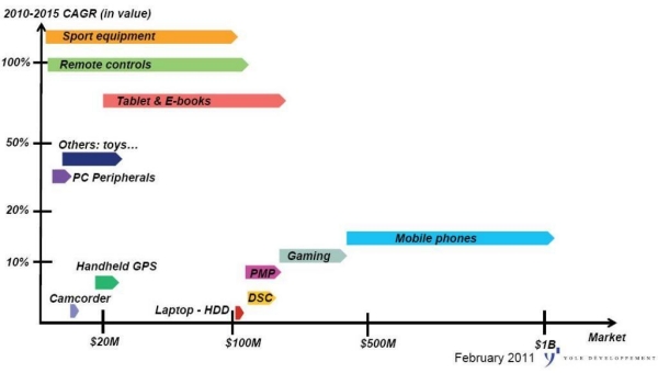
Arrows show market size evolution from 2010 to 2015.

Figure. 2010-2015 market trends for motion sensors: Accelerometers, gyroscopes, and compass for consumer and mobile applications. SOURCE: Motion Sensors for Consumer & Mobile Applications Report, 2011, Yole.

In this report, Yole Développement provides an application focus on key existing markets and promising emerging ones for motion sensing electronics: new features, technical roadmap, insight about future technology trends & challenges. This study includes market data on motion sensors for consumer & mobile products: key market metrics & dynamics.

The inertial sensor market for consumer electronics is growing very quickly due to the fast adoption of accelerometers, gyroscopes and magnetometers in mobile phones, tablets, game stations and laptops. 20.3% annual growth is expected: from $847M in 2009, the motion sensor market will reach $2.56B in 2015.

The MEMS accelerometer market will show lucrative business opportunities in coming years. This market will be strategic because many applications are expected to rely on 3-axis accelerometer + 3-axis gyroscope in a single package within 2015. There is a strong synergy between accelerometer and gyroscope technologies and players.

The gyroscope market is thriving thanks to the successful introduction of 3-axis devices by ST Micro and InvenSense. While adoption in handsets is only starting to surge, (with iPhone since June 2010 and now with Android smartphones) the gaming market is quickly growing and additional markets are emerging like tablets or remote controls.

Compasses are also gaining strong market traction. 2010 was an incredible year for digital compass in handsets, but the market will find growth outside of the mobile phone area as well: on gaming, on DSC for advanced geo-tagging, etc. It will be particularly interesting to monitor strategies of newcomers to compete against AKM, which is way ahead in the market. Competition is gaining in intensity as the motion sensing market becomes increasingly attractive. More than 50 companies are targeting this business including large players and small companies. But in the consumer market, only a few companies are really making money out of this business, while the others are struggling to make a decent profit.

Competition:

There is competition among companies trying to offer a complete product family (accelerometers, gyroscopes and magnetometers), either internally or with partners (ST is partnering with Honeywell for example on electronic compass). 

Companies cited in the report:

3DV Systems, Acer, Activision, Advancedmicrofab, Aichi Steel, AKM, Alpine, Alps Electric, Amazon, Analog Devices, Apple, ARM, Asus, Atmel, Baolab, Bosch Sensortec, Broadcom, BSkyB, Canal+, Canesta, Canon, Catapult Innovation, CEA Leti, Comcast, CSR, Dai Nippon Printing, Dalsa, Decathlon, Deep Di Semiconductor, Dell, DirecTV, Domintech, Electronic Arts, Epcos, Epson Toyocom, FreeMotion, Freescale, Fuji, Fujitsu, Futaba, Garmin, GlobalFoundries, Google, Hillcrest Labs, Hitachi, Hokuriku, Honeywell, HP, HTC, IBM, Iliad, InvenSense, ITRI, JVC, Jyve, KDDI, Kionix, Kodak, Kyocera, Lenovo, LG, Life Fitness, ogitech, , Matrix, Maxim, Mcube, Medion, Memsic, Memsmart, Memstech, MESA Imaging, Micralyne, Microchip, MicroInfinity, Microsoft, Mio, Motorola, Movea, Murata, Navteq, NEC, Nike, Nintendo, Nokia, NTT Docomo, Nuvoton Technology, Nyko, Olympus, Orbotix, Pace, Palm, Panasonic, Parrot, Pixart, PMDTechnologies, Polar, Primesense, Prolific, Qualcomm, Qualtre, RIM, Rohm, Sagem, Samsung, Sanyo, Seagate, See Technology, Senodia, Sensitec, SensorDynamics, Sharp, Sitronix Technology, Sixsens, Skyartec, SMIC, SMK, Softbank, Sony, SonyEricsson, Speedo, Sprint, SSS, ST Microelectronics, Star Trac, Sunrex, Technicolor, Technogym, TeleAtlas, TI, TomTom, Toshiba, Tronics, Trusted Positioning, TSCM, UMC, Universal Electronics, Verreon, Virtus Advanced Sensors, VTech, VTI, Wacoh, Western Digital, XSens, Yamaha, YF International, Yishay Sensors, ZillionTV, ZTE and many others.

Competition among devices: accelerometer, gyroscopes and electronic compass can provide functions, either alone or in combination with each other. So companies have to propose the best sensor or sensor combination for a dedicated function.

Competing business models: fabless companies (InvenSense for example) are competing against integrated device manufacturers (ST, Kionix, Panasonic, Epson Toyocom, Freescale). Optimization of the production cost is one of the biggest key success factors. It is thus necessary for all players to work hard in order to really get the costs lower and produce on 8" wafer lines at a reasonable yield.

Hardware competing against software: companies such as Movea start to impact the traditional supply chain model by bringing a novel expertise in software and sensor fusion.

Technology competition: companies are proposing discrete devices (a 3-axis accelerometer, a 3-axis gyroscope, etc.) or sensor combination (acceleration sensor plus gyroscope, gyroscope plus electronic compass, etc.) either in a system-in-package or on a single die, along with a transition from a sensor offer to a solution offer (with sensor fusion).

Which company, business model, device will win? Motion sensing is both a booming and fragmented market, so multiple companies can have an important part of the business. Cost-effective production infrastructure is clearly important but as the market will be moving from device to functions, the software and "function delivery" part of the business will be more and more significant.

This area is exciting and still far from being mature. "We expect considerable evolutions in the next years as illustrated by the strong demand for more precise and long-term navigation solutions, including indoor pedestrian navigation," explains Laurent Robin. In parallel to the current race to develop ultra-low cost versions of motions sensors, few start-ups are working on revolutionary motion sensing technologies by using different sensing principle or different way of combining motion sensors, with compatibility to a low-cost production infrastructure.

Laurent Robin is in charge of the MEMS & Sensors market research at Yole Développement. He previously worked at image sensor company e2v Technologies (Grenoble, France) and at EM Microelectronics (Switzerland). He holds a Physics Engineering degree from the National Institute of Applied Sciences in Toulouse. He was also granted a Master Degree in Technology & Innovation Management from EM Lyon Business School, France.
 
Yole Développement is a group of companies providing market research, technology analysis, strategy consulting, media in addition to fi nance services. With a solid focus on emerging applications using silicon and/or micro manufacturing Yole Développement group has expanded to include more than 40 associates worldwide covering MEMS and Microfluidics, Advanced Packaging, Compound Semiconductors, Power Electronics, LED, and Photovoltaic. More information on www.yole.fr

Follow Small Times on Twitter.com by clicking www.twitter.com/smalltimes. Or join our Facebook group
February 22, 2011 — A prototype implantable eye pressure monitor for glaucoma patients is believed to contain the first complete millimeter-scale computing system. And a compact radio that needs no tuning to find the right frequency could be a key enabler to organizing millimeter-scale systems into wireless sensor networks.

Researchers present papers on each today at the International Solid-State Circuits Conference (ISSCC) in San Francisco. The work is being led by three faculty members in the U-M Department of Electrical Engineering and Computer Science: professors Dennis Sylvester and David Blaauw, and assistant professor David Wentzloff.

Click to Enlarge
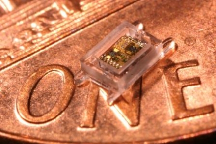
Photo: Designed for use in an implantable eye-pressure monitor, University of Michigan researchers developed what is believed to be the first complete millimeter-scale computing system. Credit: Greg Chen.

Blaauw and Sylvester’s new system is targeted toward medical applications. The work they present at ISSCC focuses on a pressure monitor designed to be implanted in the eye to conveniently and continuously track the progress of glaucoma, a potentially blinding disease. (The device is expected to be commercially available several years from now.)

In a package that’s just over 1 cubic millimeter, the system fits an ultra low-power microprocessor, a pressure sensor, memory, a thin-film battery, a solar cell and a wireless radio with an antenna that can transmit data to an external reader device that would be held near the eye.

"This is the first true millimeter-scale complete computing system," Sylvester said. "Our work is unique in the sense that we’re thinking about complete systems in which all the components are low-power and fit on the chip. We can collect data, store it and transmit it. The applications for systems of this size are endless."

The processor in the eye pressure monitor is the third generation of the researchers’ Phoenix chip, which uses a unique power gating architecture and an extreme sleep mode to achieve ultra-low power consumption. The newest system wakes every 15 minutes to take measurements and consumes an average of 5.3 nanowatts. To keep the battery charged, it requires exposure to 10 hours of indoor light each day or 1.5 hours of sunlight. It can store up to a week’s worth of information.

While this system is miniscule and complete, its radio doesn’t equip it to talk to other devices like it. That’s an important feature for any system targeted toward wireless sensor networks.

Wentzloff and doctoral student Kuo-Ken Huang have taken a step toward enabling such node-to-node communication. They’ve developed a consolidated radio with an on-chip antenna that doesn’t need the bulky external crystal that engineers rely on today when two isolated devices need to talk to each other. The crystal reference keeps time and selects a radio frequency band. Integrating the antenna and eliminating this crystal significantly shrinks the radio system. Wentzloff’s is less than 1 cubic millimeter in size.

He and Huang’s key innovation is to engineer the new antenna to keep time on its own and serve as its own reference. By integrating the antenna through an advanced CMOS process, they can precisely control its shape and size and therefore how it oscillates in response to electrical signals.

"Antennas have a natural resonant frequency for electrical signals that is defined by their geometry, much like a pure audio tone on a tuning fork," Wentzloff said. "By designing a circuit to monitor the signal on the antenna and measure how close it is to the antenna’s natural resonance, we can lock the transmitted signal to the antenna’s resonant frequency."

"This is the first integrated antenna that also serves as its own reference. The radio on our chip doesn’t need external tuning. Once you deploy a network of these, they’ll automatically align at the same frequency."

The researchers are now working on lowering the radio’s power consumption so that it’s compatible with millimeter-scale batteries.

At ISSCC, Greg Chen, a doctoral student in the Department of Electrical Engineering and Computer Science, presents "A Cubic-Millimeter Energy-Autonomous Wireless Intraocular Pressure Monitor." The researchers are collaborating with Ken Wise, the William Gould Dow Distinguished University Professor of Electrical Engineering and Computer Science on the packaging of the sensor, and with Paul Lichter, chair of the Department of Ophthalmology and Visual Sciences at the U-M Medical School, for the implantation studies. Huang presents "A 60GHz Antenna-Referenced Frequency-Locked Loop in 0.13μm CMOS for Wireless Sensor Networks." This research is funded by the National Science Foundation. The university is pursuing patent protection for the intellectual property, and is seeking commercialization partners to help bring the technology to market.

Nearly invisible millimeter-scale systems could enable ubiquitous computing, and the researchers say that’s the future of the industry. They point to Bell’s Law, a corollary to Moore’s Law. Bell’s Law says there’s a new class of smaller, cheaper computers about every decade. With each new class, the volume shrinks by two orders of magnitude and the number of systems per person increases. The law has held from 1960s’ mainframes through the 1980s’ personal computers, the 1990s’ notebooks and the new millennium’s smartphones/tablets.

"When you get smaller than handheld devices, you turn to these monitoring devices," Blaauw said. "The next big challenge is to achieve millimeter-scale systems, which have a host of new applications for monitoring our bodies, our environment and our buildings. Because they’re so small, you could manufacture hundreds of thousands on one wafer. There could be 10s to 100s of them per person and it’s this per capita increase that fuels the semiconductor industry’s growth."

The University of Michigan College of Engineering has a $180 million annual engineering research budget and 11 academic departments, numerous research centers and expansive entrepreneurial programs. Find out more at http://www.engin.umich.edu/.

Follow Small Times on Twitter.com by clicking www.twitter.com/smalltimes. Or join our Facebook group
February 21, 2011 – BUSINESS WIRE — MEMSCAP (NYSE Euronext: MEMS) (Paris:MEMS), micro-electro-mechanical systems (MEMS) technology developer, completed die-level reliability testing beyond 200 millions cycles on its Thermally Actuated Variable Optical Attenuators. MEMS based Variable Optical Attenuators are gaining momentum and market share over competing traditional technologies in optical networks applications ranging from optical modules protection to the growing segment of Power Management, according to MEMSCAP.

Recent die-level tests on the Thermally Actuated MEMS Variable Optical Attenuator product line confirmed that the MEMS devices operate within all specifications even after 200 millions cycles with all optical, mechanical and electrical properties remaining within their strict initial specifications. The key operating parameters of electrical resistance and power consumption of the units exhibit excellent stability over the full duration of the test.

Capitalizing on its optical MEMS intellectual property (IP) in design and manufacturing, MEMSCAP has developed Thermally Actuated Variable Optical Attenuators in Normally Open and Normally Closed configurations, including different die sizes, with or without metalized backside.

MEMSCAP’s Variable Optical Attenuator dies have been designed to fit most packaging technologies available on the market and are said to exhibit superior optical power attenuation stability in closed loop mode.

Fueled by the demand for faster internet connection and multiservice solutions, investments in existing and new optical network infrastructures are steadily growing to benefit the optical networking industry. Optical system integrators are looking for proven high quality and high reliability components to be safely integrated in complex optical modules operating up to 100 GBits.

Optical telecom markets are growing at a 28% CAGR from 2009 to 2014, as MEMS-based VOAs increasingly displace non-MEMS solutions, said Jérémie Bouchaud, director and principal analyst for MEMS and Sensors at IHS iSuppli (see iSuppli H2 2010 High Value MEMS Market Tracker).

MEMSCAP provides innovative MEMS-based products including components, component designs (IP), manufacturing and related services. More information on the company’s products and services can be obtained at www.memscap.com

Follow Small Times on Twitter.com by clicking www.twitter.com/smalltimes. Or join our Facebook group

February 21, 2011 — A pentaphenylene molecule sandwiched between two electrodes exhibited significantly different conductance depending on its tilt angle in relation to the electrodes. This research, carried out at Arizona State University’s Biodesign Institute and confirmed with a jiggle test, could influence nanoscale designs of telecommunications, memory, sensors, and other electronics.

In research appearing in the February 20 issue of the journal Nature Nanotechnology, Nongjian "NJ" Tao, a researcher at the Biodesign Institute at Arizona State University, has demonstrated a clever way of controlling electrical conductance of a single molecule, by exploiting the molecule’s mechanical properties.

Click to Enlarge
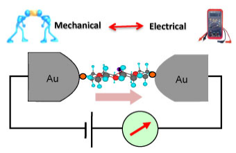
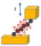
Figure 1. When electrical devices are shrunk to a molecular scale, both electrical and mechanical properties of a given molecule become critical. Specific properties may be exploited, depending on the needs of the application. Here, a single molecule is attached at either end to a pair of gold electrodes, forming an electrical circuit, whose current can be measured.

Defining and controlling the electrical conductance of a single molecule, attached to a pair of gold electrodes, is difficult at the quantum level. "Some molecules have unusual electromechanical properties, which are unlike silicon-based materials. A molecule can also recognize other molecules via specific interactions." These unique properties can offer tremendous functional flexibility to designers of nanoscale devices.

In the current research, Tao examines the electromechanical properties of single molecules sandwiched between conducting electrodes. When a voltage is applied, a resulting flow of current can be measured. A particular type of molecule, known as pentaphenylene, was used and its electrical conductance examined.

Tao’s group was able to vary the conductance by as much as an order of magnitude, simply by changing the orientation of the molecule with respect to the electrode surfaces. Specifically, the molecule’s tilt angle was altered, with conductance rising as the distance separating the electrodes decreased, and reaching a maximum when the molecule was poised between the electrodes at 90 degrees. 

Click to Enlarge

Figure 2. Atoms of a molecule (gray) are shown, with their accompanying pi orbitals (red). As the distance between electrodes is decreased, the pi orbitals can interact with the electron orbitals contained in the gold electrodes, a process known as lateral coupling. This effect increases electrical conductance through the molecule.

The reason for the dramatic fluctuation in conductance has to do with the so-called pi orbitals of the electrons making up the molecules, and their interaction with electron orbitals in the attached electrodes. As Tao notes, pi orbitals may be thought of as electron clouds, protruding perpendicularly from either side of the plane of the molecule. When the tilt angle of a molecule trapped between two electrodes is altered, these pi orbitals can come in contact and blend with electron orbitals contained in the gold electrode — a process known as lateral coupling. This lateral coupling of orbitals has the effect of increasing conductance.

In the case of the pentaphenylene molecule, the lateral coupling effect was pronounced, with conductance levels increasing up to 10 times as the lateral coupling of orbitals came into greater play. In contrast, the tetraphenyl molecule used as a control for the experiments did not exhibit lateral coupling and conductance values remained constant, regardless of the tilt angle applied to the molecule. Tao says that molecules can now be designed to either exploit or minimize lateral coupling effects of orbitals, thereby permitting the fine-tuning of conductance properties, based on an application’s specific requirements.

A further self-check on the conductance results was carried out using a modulation method. Here, the molecule’s position was jiggled in 3 spatial directions and the conductance values observed. Only when these rapid perturbations specifically changed the tilt angle of the molecule relative to the electrode were conductance values altered, indicating that lateral coupling of electron orbitals was indeed responsible for the effect. Tao also suggests that this modulation technique may be broadly applied as a new method for evaluating conductance changes in molecular-scale systems.

The research was supported by the Department of Energy (DOE) Basic Energy Science program.

In addition to directing the Biodesign Institute’s Center for Bioelectronics and Biosensors, Tao is a professor in the School of Electrical, Computer, and Energy Engineering, at ASU’s Ira A. Fulton Schools of Engineering, and an affiliated professor of chemistry and biochemistry, physics and material engineering. Tao leads a research team that studies quantum mechanics in electronics.

Courtesy of Richard Harth, science writer: The Biodesign Institute, ASU, [email protected]

Follow Small Times on Twitter.com by clicking www.twitter.com/smalltimes. Or join our Facebook group

February 18, 2011 — The market for printed electronics will be over $55 billion in 2020, according to research by IDTechEx.

Earlier roadmaps for printed electronics have been almost entirely erroneous, says Raghu Das, CEO, IDTechEx. It is not primarily about cost reduction, nor is there a trend towards organic versions taking over most applications. Combining organic and inorganic chemicals is increasingly the way to go, adds Dr Peter Harrop, chairman, IDTechEx. It is no longer focused mainly on improving existing products. Printing electronics is targeting radically different consumer products. A new ten year roadmap for printed electronics shows changes of direction with the materials, components, circuits and resulting products.

Printed electronics materials

New materials include relatively low cost, non-toxic products with electronic and electric properties for light creation to sensing of specific gases and generation of power in various ways, says Harrop.

Das points out that the introduction of printable copper by several companies last year, including Novacentrix and intinsiq, has led to a race to replace silver inks, with their price instability, in some applications such as antennas and transistor electrodes and interconnects. The alternative approach of using less silver by applying nano silver inks is also gaining traction. Much further down the line are CNT, graphene and other conductors and semiconductors offering even better performance. Currently, Heraeus is leader in organic transparent conductive inks and allied products with its Clevios brand.

Many developers in East Asia now see organic transistors improving in cost and performance too slowly to be the best solution for many high-frequency circuits in consumer goods, adds Das. For display backplanes, zinc oxide based semiconductors such as InGaZnO are prioritized for commercialization about two years after organic ones. Inkjet printed OLED TVs, RF-sputtered zinc oxide backplane transistors, printed manganese dioxide zinc batteries, printed organic transistors on a plastic substrate, and other products are being released by major electronics companies.

Printing solids is valuable, or at least printing materials that can easily be turned into solids at low enough temperatures not to damage low-cost plastic film substrates, Harrop points out. He notes that nanotubes are increasingly put down in the form of printing inks for high speed and wide area coverage.

Processing technologies

For deposition, screen and inkjet printing are the most widely deployed for printed electronics but flexo and gravure and occasionally fast letterpress are now encountered, Das asserts. Sometimes, using regular printing machines with minimal modification is in prospect. For example, organic photovoltaics and OLEDs are relatively straightforward to print but they need very good barrier sealants against oxygen and water ingress. Companies such as Henkel have new advances in this area.

Integrated systems printed roll-to-roll at low-cost render the possibility of having consumer goods as well as industrial electronic systems that are extremely compact and energy efficient, says Wolfgang Mildner, chairman of the board of directors, Organic and Printed Electronics Association.

Inkjet printing is being rapidly deployed for printing electrodes on solar cells, where non-contact deposition is desired because thinner solar cells are more fragile, Das adds.

Harrop says that much more sophisticated printing processes are being applied to next generation solid state batteries in such things as power tools and traction batteries for the electric car industry; even the electrolyte is deposited by print processes.

Flexible electronics applications in solar, semiconductors, energy storage

Samsung Electronics is prioritizing printed electronics in materials, production machines, and components and manufacturing processes. Panasonic is also seeking to deploy electronic printing much more widely, particularly for the filter and liquid crystal layers in LCDs, antennae, flexible keyboards, etc. Nokia is working on stretchable printed electronics. Oxford Photovoltaics, a company recently spun out from the University of Oxford in the UK, has developed new solar cell technology that is manufactured from cheap, abundant, non-toxic and non-corrosive materials and can be scaled to any volume. The Russians, Koreans and others are racing to make flexible color e-readers by printing both inorganic and organic layers and also composites. Large lithium-ion traction batteries can be printed for the booming electric vehicle market.

Making basic building blocks such as timers and energy harvesters with storage will be important. Consider the European FACESS project depositing a complete photovoltaic, power conversion and storage unit on a single plastic film. Army applications include printing energy harvesting layers such as the VirginiaTech CEHMS piezoelectric layers that convert movement into electricity.

GeorgiaTech has printed flexible transistor arrays using high-K inorganic gate dielectric with organic layers.

Researchers are creating a new type of solar cell designed to self-repair like natural photosynthetic systems in plants by using carbon nanotubes and DNA, an approach aimed at increasing service life and reducing cost.

Events:

IDTechEx event: Printed Electronics Europe in Düsseldorf, Germany, 5-6 April, http://www.idtechex.com/printedelectronicseurope10/en/

LOPE-C 2011 — Large-area, Organic and Printed Electronics Convention in Frankfurt, Germany, 28-30 June, www.lope-c.com

Follow Small Times on Twitter.com by clicking www.twitter.com/smalltimes. Or join our Facebook group

February 18, 2011 — A North Carolina State University endowment fund established to bridge pure research and product commercialization for entrepreneurs has awarded a $10k grant to a biomedical engineering project that will use MEMS to make catheters flexible, then stiff, for stent delivery.

The Richard L. and Marlene V. Daugherty Centennial Campus Entrepreneurialism Endowment has awarded the grant to a partnership between a NC State assistant professor in biomedical engineering and a Raleigh cardiologist. Drs. Glenn Walker and Ravish Sachar are planning to use their $10,000 award to develop a prototype for a ‘smart’ catheter.

Currently, catheters used by cardiologists do not offer enough flexibility and strength at the same time. Thus, physicians must use a combination of techniques to expertly place a catheter in the human body in order to successfully treat a clogged artery.

To overcome this problem, Walker, an assistant professor in NC State University’s department of biomedical engineering, and Sachar, a cardiologist with Wake Heart and Vascular Associates, teamed up to develop and commercialize a smart catheter that can be both flexible and strong. The catheter uses micro-electro-mechanical systems (MEMS) technology to electronically modulate catheter stiffness. It will be flexible enough to be maneuvered through winding blood vessels and positioned near the affected area, but it can also be stiffened to allow the delivery of a stent to the lesion site. This reduces the chances of injury to the patient during the procedure by reducing the number of catheters and guide wires that must be used.

The endowment is named after the retired IBM executive who ran the company’s RTP operations for 23 years, and his wife. Daugherty is a trustee of the Kenan Institute at NC State, as well as a board member for NC State’s Entrepreneurship Initiative. Daugherty was also Director of the Research Corporation for NC State’s Centennial Campus and board member of Progress Energy. He received the North Carolina Public Service Award in 1991 and the Raleigh Chamber of Commerce’s A.E. Finley Award in 1994.

Centennial Campus is a research park and technology campus owned and operated by North Carolina University. Home to more than 60 corporate, government and non-profit partners, such as Red Hat, ABB, and the USDA, collaborative research projects vary from nanofibers and secure open systems technology to serious gaming and biomedical engineering. Four university college programs also have a significant presence on campus – College of Engineering, College of Veterinary Medicine, College of Textiles and the College of Education. Learn more at http://www.centennial.ncsu.edu

Follow Small Times on Twitter.com by clicking www.twitter.com/smalltimes. Or join our Facebook group