Category Archives: Materials and Equipment

(July 21, 2010) — The Institute of Microelectronics (IME), a research institute of the Agency for Science, Technology and Research (A*STAR), announced a collaborative partnership with Stanford University to develop silicon-nanowire-based circuits that are inspired by the brain. Under the research collaborative agreement, IME and Stanford will jointly develop silicon nanowire based neuromorphic computational elements (silicon neurons) that take advantage of the capabilities of nanowire technology.

The quest to come up with an artificial system organized like the biological nervous system promises to drive the future of humanoid robots and supercomputers that can perform highly complex decision-making for gaming and defense technologies. The electronics systems using neuromorphic designs aim to work like the biological nervous system. The collaboration represents a further expansion of the extensive neuromorphic computing activities at Stanford University and provides a new application opportunity for nanowire transistors developed at IME.

The partnership leverages on the relative strengths of the respective institute. IME is a leading laboratory in the fabrication of nanowire transistors, with considerable progress reported in recent years, including the demonstration of functional circuits. Stanford University has a leading group in neuromorphic engineering, an approach to designing systems that work like the brain.

The joint project will be led by Dr Navab Singh, Principal Investigator of the NanoElectronics section at IME, and Associate Professor Kwabena Boahen, Director of the Brains In Silicon group at Stanford University. The project will tap Stanford University’s expertise in neuromorphic design to model and design silicon neuron circuits.  The circuits will be fabricated by IME using state-of-the-art nanowire technology, more specifically, the lateral gate-all-around FUSI gate transistor technology.

“The gate all around (GAA) transistors based on silicon nanowires are considered the most promising alternatives to scaling limitations of planar CMOS technology — foundation of today’s electronics. Nanowire transistors offer near ideal subthreshold behaviour, low off state leakage, and high drive current — all the characteristics required to enable a highly integrated design that works with little power, much like the real brain. On the other hand, due to nanowire’s structure and strong response in respect to tiny change in dimension, nanowire transistors also exhibit increased variability, strong low frequency and telegraph-style noise that are interesting to niche applications,” said Dr Singh.

On the unique characteristics of nanowire transistors, Associate Professor Boahen said, “Our joint mission is to develop revolutionary architectures that would be tolerant to, or better yet, thrive under the variability and noise. Interestingly, variability and noise are key elements of a biological brain.”

Professor Dim-Lee Kwong, executive director of IME, said, “IME’s alliance with Stanford University to develop neuromorphic test circuits will be a window to the future of an emerging discipline that is expected to have a ripple effect on a broad spectrum of industries.”

The Institute of Microelectronics (IME) is a research institute of the Science and Engineering Research Council of the Agency for Science, Technology and Research (A*STAR) of Singapore. A*STAR oversees 14 biomedical  sciences, and physical sciences and engineering research institutes, and seven consortia & centre, which are located in Biopolis and Fusionopolis, as well as their immediate vicinity. For more information about A*STAR, visit www.a-star.edu.sg

Also read:

Fully gate-all-around silicon nanowire CMOS devices

Although CVD-grown nanowires are good for demonstration purposes, getting them into manufacturing calls for the utilization of CMOS fabrication methods … (Solid State Technology, 2008, Volume 51, Issue 5, co-authored by Dr. Navab Singh and Professor Dim-Lee Kwong)

Toshiba tips Si nanowires for 16nm chips

Presenting at the VLSI Symposium, Toshiba says it has developed a silicon nanowire transistor with vastly improved on-current levels, targeting 16nm and beyond system LSIs … (Small Times, 2010, online issue)

(July 20, 2010) — Nextreme Thermal Solutions will now include materials evaluation and characterization services in its consulting portfolio. With recent advances in materials sciences and nanotechnology, new materials are being developed that exhibit thermoelectric properties.

The assessment of thermoelectric materials is a challenge, particularly when investigating them over significant temperature ranges. Nextreme has capabilities to conduct measurements across a range of temperatures, below 200K to above 700K. Properties that can be measured include Seebeck coefficient, electrical resistivity and thermal conductivity. Equipped with thermal modeling, design, and engineering consulting services, Nextreme’s team of engineers can accelerate the development of new applications that are currently thermally constrained.

In addition to the evaluation of materials, Nextreme offers thermal modeling, design and engineering services to deliver fully optimized thermal management solutions. Nextreme routinely conducts analytical and numerical thermal modeling at all design levels from component to module to subsystem. Design services range from rudimentary analysis such as 1D and 3D modeling to more complex analyses that may involve the use of passive heat rejection systems, such as heat sinks and exchangers, or the use of active devices such as thermoelectric coolers to solve the overall thermal problem. Advanced analysis of complex systems, components or packages often require more detailed modeling to understand heat flow and thermal gradients.

The use of Nextreme’s engineering services can enable rapid and successful prototyping and accelerate a program as well as reduce program delays. Services are tailored to needs and budget. "Initial evaluation and integration of micro-scale thermoelectrics is often a challenge for organizations without thermal engineering expertise or when existing resources are limited," said Dave Koester, VP of engineering at Nextreme.

Nextreme uses its thin-film thermoelectric technology to produce discrete and integrated cooling and power generation devices. Nextreme currently offers several thermoelectric coolers, such as the OptoCooler HV14 and UPF40, that are capable of cooling and heating in ranges from 0.4 to 4W, with plans to provide higher heat pumping in the near future. Modules for electronics cooling and power generation are available for order now and pricing is available upon request. Nextreme Labs is currently working in laser diode cooling, thermal margining, and clean energy harvesting solutions for wireless sensor networks and remote power management. For more information, go to www.nextreme.com.

(July 19, 2010) — A confluence of new piezo-based technology has added new capability into the nano- and micro-positioning world. The global market for piezoelectric-operated actuators and motors was estimated to be $6.6 billion in 2009 and is estimated to reach $12.3 billion by 2014, showing an AAGR of 13.2%/year.

Figure. Global share for piezoelectric actuators and motors by application, 2009 and 2014 ($ millions).
Click to Enlarge

Piezo actuation is increasingly suitable for applications formerly addressable only by magnetic motors, and the technology offers significant benefits in terms of size, speed, fieldlessness, reliability, vacuum compatibility, resolution and dynamics. These benefits, in turn, enable significant advances in existing and new applications. Piezomotors and actuators typically eliminate any need for gear reduction because they drive loads directly. Piezoelectric actuators have been commercialized in various areas such as information technology, robotics, biomedical engineering, automotive, ecological and energy engineering.

According to a recently published report from iRAP, Inc., ET112: Piezoelectric Actuators and Motors – Types, Applications, New Developments, Industry Structure and Global Markets, the global market for piezoelectric-operated actuators and motors was estimated to be $6.6 billion in 2009 and is estimated to reach $12.3 billion by 2014, showing an average annual growth rate (AAGR) of 13.2% per year.

The market for piezoelectric-operated actuators and motors in ultra-small scale precision motion related applications will be the largest segment, estimated to have reached $3,200 million (48.6% share) in 2009 and projected to reach $6,000 million in 2014, for an AAGR of 13.4%. The other major segment includes phone cameras, digital cameras, microscope lenses, mirrors and optics, estimated at $2,800 million (42.5% share) in 2009 and $5,200 million in 2014, for an AAGR of 13.1%.

The remaining 8.9% ($587 million) is a third market segment consisting of auto fuel injectors, micro-pumps, micro-blowers, printer cartridges, surgical instruments, mini-robots, etc.). In 2014, this market segment will have a share of 8.7% ($1,090 million).

Table. Global market size/percentage share for piezoelectric actuators and motors by application, through 2014 (Source: iRAP, Inc.)

Applications

2009 ($ Mil.) 2009 (%) 2014 ($ Mil.) 2014 (%)

AAGR (%)
2009-14

Ultra-small scale motion related applications 3,200 48.6 6,000 48.9 13.4
Cameras, microscope lenses, mirrors and optics     2,800 42.5 5,200 42.4 13.1
Others, e.g., auto fuel injectors, micro-pumps, micro-blowers, piezo ink cartridges, surgery instruments, mini-robots 587 8.9 1,090 8.7 13.1
Total  6,587 100 12,290 100 13.2

The manufacturers of optics, photonics and nanometrology equipment have been the major consumers of piezoelectric-operated motors and actuators.

Life sciences and medical technology also constitute a high-growth segment of the piezoelectric-operated actuators and motors market. This area is expected to grow at 18.7% annually and could record an even higher growth rate if there is wider acceptance by end users. It is still going through a gestation period. Read more about the life sciences and medical sector.

Over the projected period of five years, market share of piezoelectric-operated actuators and motors will increase, taking share from electromagnetic motors.

In terms of types, bulk PZT material-based piezo actuators and motors have the highest market share at 98%, with a market of US$6.455 billion in 2009; this segment will grow at an AAGR 12.4% to reach US$11.6 billion in 2014. Thick-film PZT used in piezo actuators and motors reached a market of US$65.83 million in 2009, approximately 1% of the total, and will show an AAGR of 30.1% to reach US$245.8 billion in 2014. Fiber composites used in actuators and motors had a market of US$39.52 million in 2009, and by 2014, with an AAGR of 50.7 %, the segment will reach US$307.2 million in sales. Lead-free ceramics used in actuators and motors had a market of US$26.345 million in 2009 and is expected to reach US$123 million by 2014, for an AAGR of 36%.

In terms of regional market share, North America leads, with 40.5% in 2009, followed by Europe with 34%, Japan with 20%, and the balance 5.5% for China and the rest of the world.

For more information from iRAP, Inc., visit http://www.innoresearch.net/report_summary.aspx?id=75&pg=154&rcd=ET-112&pd=7/1/2010

(July 16, 2010) — SEMICON West 2010 wrapped this week in San Francisco. This article includes JC Kim, SEMI Board of Directors Chair, discussing the show and the semiconductor industry future. We also have POVs from the show floor by the ElectroIQ.com bloggers.

JC Kim, Edwards Vacuum and chair of SEMI Board of Directors, celebrates the upturn in the semiconductor and packaging industry. Next year is expected to increase the positive business environment.

More from SEMICON West: 

SEMICON West, Day 1: CMP, slurries, metrology, thermal, zombies, observations

Techcet’s Michael Fury reports from Day 1 of SEMICON West, from keynotes to CMP to thermal characterization, and the continued use of “zombie” semiconductor manufacturing technologies.

SEMI: Materials bounce back to records, but slowing in 2010 

Unit shipments of key semiconductor materials are already back to record levels just a year after the most punishing period in the industry’s history, but the growth will slow in 2011 for several reasons, according to the latest forecast data presented at SEMICON West.Click to Enlarge

POVs on the Advanced Semiconductor Manufacturing Conference (ASMC) poster presentations

ElectroIQ.com’s senior technical editor Debra Vogler recorded a few of the reactions Sunday night at the interactive poster presentations, part of the Advanced Semiconductor Manufacturing Conference, taking place alongside SEMICON West this week in San Francisco.

A BlaSST from the Past

Stop reading! Unless you want to join me in reminiscing about the old days of Semicon West. Every time I’m about to head out, I have to think back to — egad — 1982 when I first attended. That makes this #29 for me.

(July 14, 2010) — In this video from SEMICON West 2010, Marcus Wimplinger, EV Group, summarizes the results of SEMATECH work using EVG’s 300mm bonding systems that enables submicron alignment. Highly accruate wafer bonding is used for Cu-to-Cu bonding and other packaging applications. Here, he speaks with senior technical editor Debra Vogler.

See all the latest from SEMICON West 2010 at: http://www.electroiq.com/index/Semiconductors/semiconwest2010.html

Read "Lithography and wafer bonding solutions for 3D integration," co-authored by Wimplinger, from Advanced Packaging, March 2010. Also attend the on-demand webcast presented by EVG, It’s Time For 3D Now – TSV Process Achievements

(July 14, 2010) — Rice University scientists have found the ultimate solvent for all kinds of carbon nanotubes (CNTs), a breakthrough that brings the creation of a highly conductive quantum nanowire closer.
 
Nanotubes have the frustrating habit of bundling, making them less useful than when they’re separated in a solution. Rice scientists led by Matteo Pasquali, a professor in chemical and biomolecular engineering and in chemistry, have been trying to untangle them for years as they look for scalable methods to make exceptionally strong, ultralight, highly conductive materials that could revolutionize power distribution, such as the armchair quantum wire.
 
The armchair quantum wire — a macroscopic cable of well-aligned metallic nanotubes — was envisioned by the late Richard Smalley, a Rice chemist who shared the Nobel Prize for his part in discovering the the family of molecules that includes the carbon nanotube. Rice is celebrating the 25th anniversary of that discovery this year.
 
Pasquali, primary author Nicholas Parra-Vasquez and their colleagues reported this month in the online journal ACS Nano that chlorosulfonic acid can dissolve half-millimeter-long nanotubes in solution, a critical step in spinning fibers from ultralong nanotubes.
 
Current methods to dissolve carbon nanotubes, which include surrounding the tubes with soap-like surfactants, doping them with alkali metals or attaching small chemical groups to the sidewalls, disperse nanotubes at relatively low concentrations. These techniques are not ideal for fiber spinning because they damage the properties of the nanotubes, either by attaching small molecules to their surfaces or by shortening them.
 
A few years ago, the Rice researchers discovered that chlorosulfonic acid, a "superacid," adds positive charges to the surface of the nanotubes without damaging them. This causes the nanotubes to spontaneously separate from each other in their natural bundled form.
 
This method is ideal for making nanotube solutions for fiber spinning because it produces fluid dopes that closely resemble those used in industrial spinning of high-performance fibers. Until recently, the researchers thought this dissolution method would be effective only for short single-walled nanotubes.
 
In the new paper, the Rice team reported that the acid dissolution method also works with any type of carbon nanotube, irrespective of length and type, as long as the nanotubes are relatively free of defects.
 
Parra-Vasquez described the process as "very easy."
 
"Just adding the nanotubes to chlorosulfonic acid results in dissolution, without even mixing," he said.
 
While earlier research had focused on single-walled carbon nanotubes, the team discovered chlorosulfonic acid is also adept at dissolving multiwalled nanotubes (MWNTs). "There are many processes that make multiwalled nanotubes at a cheaper cost, and there’s a lot of research with them," said Parra-Vasquez, who earned his Rice doctorate last year. "We hope this will open up new areas of research."
 
They also observed for the first time that long SWNTs dispersed by superacid form liquid crystals. "We already knew that with shorter nanotubes, the liquid-crystalline phase is very different from traditional liquid crystals, so liquid crystals formed from ultralong nanotubes should be interesting to study," he said.
 
Parra-Vasquez, now a postdoctoral researcher at Centre de Physique Moleculaire Optique et Hertzienne, Université de Bordeaux, Talence, France, came to Rice in 2002 for graduate studies with Pasquali and Smalley.
 
Study co-author Micah Green, assistant professor of chemical engineering at Texas Tech and a former postdoctoral fellow in Pasquali’s research group, said working with long nanotubes is key to attaining exceptional properties in fibers because both the mechanical and electrical properties depend on the length of the constituent nanotubes. Pasquali said that using long nanotubes in the fibers should improve their properties on the order of one to two magnitudes, and that similar enhanced properties are also expected in thin films of carbon nanotubes being investigated for flexible electronics applications.
 
An immediate goal for researchers, Parra-Vasquez said, will be to find "large quantities of ultralong single-walled nanotubes with low defects — and then making that fiber we have been dreaming of making since I arrived at Rice, a dream that Rick Smalley had and that we have all shared since."
 
Co-authors of the paper are graduate students Natnael Behabtu, Colin Young, Anubha Goyal and Cary Pint; Pulickel Ajayan, the Benjamin M. and Mary Greenwood Anderson Professor in Mechanical Engineering and Materials Science and of chemistry, and Robert Hauge, a distinguished faculty fellow in chemistry, all at Rice; and Judith Schmidt, Ellina Kesselman, Yachin Cohen and Yeshayahu Talmon of the Department of Chemical Engineering, Technion-Israel Institute of Technology, Haifa, Israel.
 
The Air Force Office of Scientific Research, the Air Force Research Laboratory, the National Science Foundation Division of Materials Research, the Robert A. Welch Foundation, the United States-Israel Binational Science Foundation and the Evans-Attwell Welch Postdoctoral Fellowship funded the research.
 
Read the abstract at http://pubs.acs.org/doi/abs/10.1021/nn100864v

by James Montgomery, news editor

July 13, 2010 – Innovation drives everything — and innovation spawned from the semiconductor and related industries is poised to do nothing less than change the world, or at least help everyone adapt better to it, as related by Bernie Meyerson of IBM, in SEMICON West’s opening keynote address on Tuesday morning.

The concept of innovation has significance at IBM — each year in an "Innovation Jam" it asks all employees to tell, basically, what big issues are important to them, and from that figure out what challenges can be addressed and solved with technology. Examples:

Water. In the US, 36 states foresee a water shortage (a top-of-mind theme to a show in California!). And two-thirds of cities in China are already there.

Traffic.
Meyerson’s slide showed a photo of paralyzing traffic jam in just one "small business district" in Los Angeles — and how things are worse in places like Rome and Beijing — and how traffic problems lead to huge amounts of lost time, wasted gas, tons of carbon emissions, all translated into billions of dollars.

Food.
A typical carrot travels 1600 miles to its final destination, other foods hundreds of miles. And $48B worth of food is simply thrown away.

Healthcare.
2.2M errors in dispensing medications occur simply because the prescription is misread.

The common theme among all these areas, Meyerson summed, is they are largely caused by too much or not enough information. Thus, he proposed, applying IT can help create a "smarter planet" to solve them. And this touches our industry in a handful of ways: semiconductors (logic, memory, storage), sensors, energy, etc. Our industry has a good track record at meeting challenges and pushing the envelope — over the last hundred years, there’s been a 100 improvement in what $1k can get in technology (battery developers are happy today with an 8× improvement!).

And the challenges are significant. Sequencing the genome in and of itself isn’t a revolutionary world-changing thing, Meyerson suggested — "but sequencing the genome for $80 — that’s revolutionary!"

Turning his attention specifically to advancements in semiconductors, he addressed the problems with Moore’s Law and scaling silicon, and how efforts to find answers have "lit up" the periodic table, which has also greatly increased complexities and costs. Some technologies are being investigated and show promise (e.g, nanowires, carbon nanotubes, and graphene), but none are ready to scale to making billions of devices.

Meeting challenges isn’t just about improving devices. "The speed of life is dreadfully slow," he said — specifically, it’s 3×10⁸ m/s. In football field-sized data centers, it takes lots of cycles (and power too) just to fetch data from a server 100m away. 3D can change that equation to just 100μm, he noted.

Radical collaboration, system-level innovation

Since finding new ways to develop technology will involve bumping up against fundamental rules of physics, industry has come around to the need to combine intellectual as well as financial capital in "radical collaborations" — such as has been done with the IBM-led Common Platform Alliance, in which companies with the same base technology go out and compete for customers. Such a model has made it into the course teachings at Harvard Business School, Meyerson noted.) Such collaboration has to come in the face of such massive numbers vs. the past. There will be a projected 2B people on the Internet, which has been a popular flag to wave as representative of demand — but it’s the "Internet of things," devices that produce and share data, which will be the real drivers, he noted. Consider: there will be 33B RFID tags, all wanting to "talk" to IT. And overall, a trillion various types of Internet-connected devices.

One area that can take advantage of cloud-computing, application specific methodology, one that can be highly utilized for batch workloads, and prioritize jobs in real-time, is EDA. Meyerson showed how IBM has created a "design cloud" with 20,000 cores, 150+TB RAM, and 3000 users, and figured out how to intelligently manage system workload so that utilizations are maximized — a slide showed a 48-hr map where system utilization was "steadfastly" above 90%.

Addressing the aforementioned global "human" challenges (water, etc.) will require just such system-level innovations, "holistic designs," Meyerson said. One example: "stream computing," essentially real-time continuous digestion and analysis of data from numerous sources, all funneled to a person (or decision tree) to make an informed decision. Consider a commodities trader pulling information from the NYSE, SEC, video news, and weather data to calculate proper buying (or selling) of oranges, with <1msec latency. TD Bank, he said, is already doing this to identify and execute trades, with <150μm latency. For a healthcare spin, a group in Ontario is using this methodology to identify infants in various ways, ultimately able to predict onset of a particular dangerous affliction a full 24hrs before a trained ICU nurse.

Another example of an intelligent "systems of systems": transportation. Generally speaking, conventional operation is to compile transaction data, e.g. tollbooths. Beyond that, systems could determine who crossed the point of toll, where, and how fast, and from this proactive traffic models could be devised. Ultimately the system could be optimized to take that data into account and build pricing models and even citywide infrastructures. Meyerson showed a correlation of traffic volume and speed, where 10-min ahead forecasts and real-time data tracked basically into identical trend lines. Such a system is already being established in Singapore, he noted.

Such system-level activity — not discrete differentiators — will define the "winners" in just the next five years, Meyerson suggested.

Quips

An engineer joke, courtesy of Meyerson: What happens when an engineer gets his hand caught in a door? He pries it out, and then sticks his other hand in to get a second set of data.

Technology development isn’t just complex and costly, it can be downright ugly. Meyerson showed a photo of the EUV lithography tool currently operating at Albany Nanotech. Not only does it cost roughly $100M, but, he said, it looks like "someone took an electromagnet through an auto junkyard."

July 12, 2010 – Unit shipments of key semiconductor materials are already back to record levels just a year after the most punishing period in the industry’s history, but the growth will slow in 2011 for several reasons, according to the latest forecast data presented at SEMICON West.

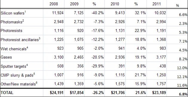
The total semiconductor materials market will grow 21.6% in 2010 to $21.71B (vs. -26.2% in 2009, $17.854B), said Dan Tracy, presenting at the Gartner-hosted Monday afternoon symposium. Look for this to slow to 6.8% in 2011 to $23.19B. (But still not at 2008 levels of $24.19B.)

Best growth in 2010: Silicon wafers (32% to $9.41B), followed by photoresists (23%, $1.13B) and CMP slurry/pads (21.7%, $1.11B). Wafers also represented the biggest turnaround from 2009, when they suffered a -40% decline. Projected 25% growth in wafer unit shipments this year could end up approaching 31%-32%, Tracy said (2Q area shipments were up at least 5% sequentially). There’s demand for 200mm wafers too, as capacity brought offline in 2007-2008 is now being brought back online for analog and discrete use. Even 6-in. wafer demand was up 20% through May, he pointed out.

"Wafer suppliers saw very steep erosion" in the downturn, Tracy pointed out. "They want to regain pricing strength in 2010."

Lowest growth in 2010, in single-digits, will be seen in wet chemicals (4.0%, $941B), photomasks (7.1%, $2.93B), and sputter targets (9.8%, $391B). Others are respectably in the teens.

As things slow into 2010, look for single-digits in the big categories (wafers, gases, photomasks/resists/ancillaries), but around 12% growth for CMP, sputter targets, and other/new materials. 

Click to Enlarge

(Source: SEMI)
1 Silicon wafers include merchant sales value only; includes SOI wafers; no reclaim wafers 
2 Includes captive market 
3 Includes resist removal chemicals, developers, anti-reflective coatings, contrast enhancers, edge bead removers, adhesion promoters, etc. 
4 Source is Techcet Group LLC, includes precious metals 
5 Estimates for IC applications only 
6 Includes low-k dielectrics, copper plating solutions, dielectric precursors, organometallic precursors, etc. 

Narrowing in on specific segments:

Photoresist chemicals. SEMI projects 23% growth in this segment in 2010. 193nm resists, which make up 40% of the market, will reach $450M in 2010 and ~$500M in 2011. They’ll continue to be used down to 22nm, Tracy noted; critical layers will have a resist uniquely "tuned" and produced for a specific device, process, or layer.

Photoresist chemicals. Look for 19% growth here in 2010, and 26% growth for removal materials. This sector’s CAGR from 2003-2010 (17%) is more than double the rate for fab materials.

Reclaim wafers. After surging from 2004-2007 and losing most of that volume over the past couple of years, reclaim wafer shipments are inching back up again, to around $300M this year. But ASPs, which started the same period at >$0.35/sq. in, have steadily declined, and are expected to barely stay flat from 2009-2011. Key issues: overcapacity for 300mm wafer claim; scrap silicon revenue has essentially dried up; and the variability and complexity of materials on wafers are more difficult to clean. five players exited the market during the downturn, Tracy said. As polysilicon suppliers ramped up product to fill growing need from PV solar, reclaim wafers lost that market inroads. As fabs and foundries fill up and utilization rates stay high, things should improve for silicon wafer reclaim suppliers.

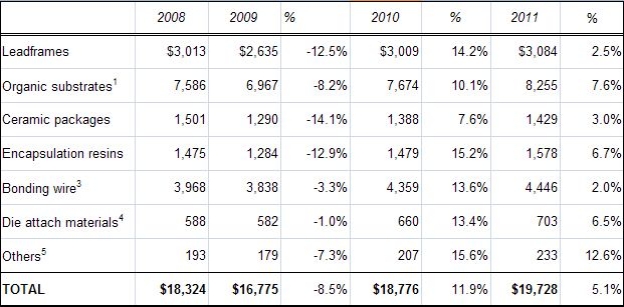
Packaging materials won’t have quite as good a year overall in 2010 as the overall sector, but it will be respectable with growth in the low teens both overall and in most segments, and could approach 15%, Tracy said — bookings through the half-year are already ahead of all billings through 2009. Top growth and best bounceback goes to encapsulation resins, and expect strong growth in organic substrates. Growth (in dollars) for bonder wire largely reflects the steep climb in the price of gold, though shipments also are growing steadily. Wire bond was 5.9% of 2009 shipments, twice what they were in 2008, and will reach 10% this year and 12%-13% in 2011.

For 2011 packaging materials also will see a slowdown to single-digit growth, though the "others" category — which includes things like wafer-level package dielectrics and solder balls — will stay in the low-teens. Note bonding wire lags the sector in 2011, barely eking out any growth at all (2%), just ahead of leadframes (although leadframe unit shipments have already surpassed pre-downturn levels). 

Click to Enlarge

(Source: SEMI)
1 Source is TechSearch International. Includes PBGA, PPGA, LGA, and CSP laminate substrates and flex BGA and CSP substrates
2 Assume gold value of $660/trz for 2007, $872/trz for 2008, $920 for 2009-2011 forecast period
3 Includes die attach film (tape) materials 
4 Other includes solder balls and wafer level package dielectrics 

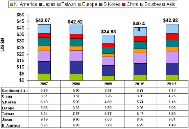
By region, Japan remains the largest installed capacity base, and there’s a lot of advanced packaging happening there too, Tracy pointed out. Taiwan also is strong due to its packaging houses and 300mm facilities. And three-quarters of China’s market are for packaging materials, as players move to advanced packaging technologies — that region actually grew in the lousy 2009 environment, Tracy pointed out.
 

Click to Enlarge

Materials forecast by region. (Source: SEMI)


(July 9, 2010) — Metallic carbon nanotubes (CNT) show great promise for applications from microelectronics to power lines because of their ballistic transmission of electrons. But magnets can stop those electrons in their tracks.

Rice physicist Junichiro Kono and his team have been studying the Aharonov-Bohm effect — the interaction between electrically charged particles and magnetic fields — and how it relates to carbon nanotubes. While doing so, they came to the unexpected conclusion that magnetic fields can turn highly conductive nanotubes into semiconductors.

Click to Enlarge

Their findings are published online this month in Physical Review Letters.

"When you apply a magnetic field, a band gap opens up and it becomes an insulator," said Kono, a Rice professor in electrical and computer engineering and in physics and astronomy. "You are changing a conductor into a semiconductor, and you can switch between the two. So this experiment explores both an important aspect of the results of the Aharonov-Bohm effect and the novel magnetic properties of CNTs."

Kono, graduate student Thomas Searles, and their colleagues at the National Institute of Standards and Technology (NIST) and in Japan successfully measured the magnetic susceptibility of a variety of nanotubes for the first time; they confirmed that metallics are far more susceptible to magnetic fields than semiconducting nanotubes, depending upon the orientation and strength of the field.

Single-walled nanotubes (SWNTs) — rolled-up sheets of graphene — would all look the same to the naked eye if one could see them. But a closer look reveals nanotubes come in many forms, chiralities, depending on how they’re rolled. Some are semiconducting; some are highly conductive metallics. The gold standard for conductivity is the armchair nanotube, so-called because the open ends form a pattern that looks like armchairs.

Kono and Searles traveled to the Tsukuba Magnet Laboratory at the National Institute for Materials Science (NIMS) in Japan, where the world’s second-largest electromagnet was used to tease a refined ensemble of 10 chiralities of SWNTs, some metallic and some semiconducting, into giving up their secrets.

By ramping the big magnet up to 35 tesla, they found that the nanotubes would begin to align themselves in parallel and that the metallics reacted far more strongly than the semiconductors. (For comparison, the average MRI machine for medical imaging has electromagnets rated at 0.5 to 3 tesla.) Spectroscopic analysis confirmed the metallics, particularly armchair nanotubes, were two to four times more susceptible to the magnetic field than semiconductors and that each chirality reacted differently.

The nanotubes were all about 0.7 to 0.8 nanometers (or billionths of a meter) wide and 500 nanometers long, so variations in size were not a factor in results by Searles. He spent a week last fall running experiments at the Tsukuba facility’s "hybrid," a large-bore superconducting magnet that contains a water-cooled resistive magnet.

Kono said the work would continue on purified batches of nanotubes produced by ultracentrifugation at Rice. That should yield more specific information about their susceptibility to magnetic fields, though he suspects the effect should be even stronger in longer metallics. "This work clearly shows that metallic tubes and semiconducting tubes are different, but now that we have metallic-enriched samples, we can compare different chiralities within the metallic family," he said.

Co-authors of the paper include Yasutaka Imanaka and Tadashi Takamasu of NIMS, Tsukuba, Japan; Hiroshi Ajiki of the Photon Pioneers Center at Osaka University, Japan; and Jeffrey Fagan and Erik Hobbie, researchers at NIST, Gaithersburg, Md.

Searles conducted the majority of the research during a visit to NIMS supported in part by a National Science Foundation Partnerships for International Research and Education grant to Kono and his co-principal investigators. Other funding came from the Department of Energy Office of Basic Energy Sciences, the Robert A. Welch Foundation and the Grant-in-Aid for Scientific Research from the Ministry of Education, Culture, Sports, Science and Technology of Japan.

Read the abstract here: http://prl.aps.org/abstract/PRL/v105/i1/e017403

Read more about semiconductors here

Read more about carbon nanotubes here

(July 7, 2010) — Multitest expanded the portfolio of its Singapore spare parts distribution center for pogo pin-based test contactors. With this step, all major spare parts for semiconductor package test handlers and contactors are now available for fast delivery to Asian package test sites.

The regional distribution center is a part of Multitest’s S3 program: Superior Spares Support. Together, with the recently launched e.services (an online spare part information and planning tool), the Singaporean distribution center significantly contributes to the smooth supply of spare parts.

All Asian customers will automatically benefit from this regional approach. By registering for e.services, customers will receive all of the benefits of Multitest’s S3 program.

Multitest is a manufacturer of test equipment for semiconductors: test handlers, contactors, and ATE printed circuit boards. For more information about Multitest’s eServices, visit www.multitest.com/e.services