Category Archives: Materials and Equipment

SWeNT gets grants for new CNTs


December 18, 2009

December 18, 2009 – Southwest Nanotechnologies Inc. (SWeNT) has received two grants from the Oklahoma Center for the Advancement of Science and Technology, to help develop new single-walled carbon nanotubes (CNT) with improved electrical conductivity and transparency.

Under one of the grants, coming through the Oklahoma Applied Research Support (OARS) program, SWeNT will develop materials targeted for use in CNT-printed electrodes for next-generation LED lighting applications that consume up to a third less power; other applications beyond LED lighting could include photovoltaics, supercapacitors, batteries, and displays, according to SWeNT CEO David Arthur. The grant amount was not disclosed, though OARS describes its program’s funding levels in two types: $10K-$45K (1-2 years) or $300K (1-3 years), 1:1 matched.

The other grant, pegged at about $60K, will bring in three undergraduate interns to help work on current projects at SWeNT.

"OCAST’s support for our employment of interns to assist us in new technology development will help us on the OARS activity as well as other research activities we have planned," Arthur said in a statement, adding that "SWeNT would not be a leading carbon nanotubes producer today without OCAST support."

December 17, 2009–The IMAPS-UK MicroTech-2010 and IEEE-CPMT Advanced Packaging Materials (APM), to be held Feb. 28 through March 2 at Cambridge University, is being billed as the major spring 2010 event on electronics packaging, interconnection, and integration in Europe.

MicroTech-2010 will highlight disruptive technologies and APM featuring advanced polymer, organic ,and inorganic materials, and will include keynote talks, technical presentations, and exhibits designed to provide leading-edge coverage of developments in all areas of packaging materials and processes. This event will be held at Cambridge University’s Møller Centre, located near many new and established AP-related companies.

APM, Polytronic and MicroTech are major packaging materials forums, providing opportunities to network and meet leading experts and exchange up-to-date packaging knowledge in the field.

December 14, 2009 –  Researchers at Stanford disclosed their latest work at this year’s International Electron Devices Meeting (IEDM) on combining carbon nanotubes (CNT) and logic circuits to devise new techniques for preventing flaws and building multilayer chip prototypes. The transistors are said to be grouped in the same "cascading" sequences as for computational logic and memory, with processes compatible with standard industrial-scale VLSI (very large scale integration) manufacturing.

"Carbon nanotube transistor technology has moved beyond the realm of scientific discovery and into engineering research," stated H.-S. Philip Wong, professor of electrical engineering at Stanford and a co-author of the paper. "We are now able to construct devices and build circuits on a wafer scale as opposed to previous ‘one-of-a-kind’ type demonstrations."

The chips employ two techniques already developed at Stanford: one (invented in 2007) to enable working transistors regardless of whether the CNTs are straight, and another (invented in 2008) to enable VLSI-scale fabrication of nanotube transistors on a chip. A third, newly developed technique announced at this year’s IEDM is a process for reliable removal of "metallic" CNTs that can conduct electrical current and short-circuit transistors. This technique, dubbed "VLSI-compatible metallic nanotube removal" (VMR), makes practical a previous idea (from Paul Collins and IBM colleagues, circa 2001) to break up the CNTs by exposing them to light, by creating a grid of electrodes to "zap" them away; this same grid can then be etched to produce any circuit design.


An electron microscope image showing carbon nanotube transistors (CNTs) arranged in an integrated logic circuit. (Source: Stanford)

Another IEDM disclosure from Stanford follows up on the VMR work by creating the first multilayer CNT 3D integrated circuit. 3D circuits are already being stacked and connected with conventional chipmaking materials, but the new research shows it can be done with CNTs integrated from the start as a 3D design that yields a higher density of connections among the layers. A prototype three-layer chip with dozens of CNT transistors were connected in functioning gates by nanotube and metal wiring — key to the achievement was a "relatively low-temperature process" that transfers CNTs from a quartz wafer onto a silicon chip.

Still a challenge is to increase the number of CNTs that can be patterned onto a given area on the chip, to thus scale up to modern chip design complexity of millions of transistors. The Semiconductor Research Corporation’s Focus Center Research Program and the National Science Foundation helped fund the research.

December 14, 2009 – The Supervisory Council of the Russian Corporation of Nanotechnologies (RUSNANO) recently approved two new measures: one for producing concentrated photovoltaic technology, and participation in work to develop porous nanostructured nonmetallic coatings.

In the former, RUSNANO aims to commercialize research coming out of the Ioffe Physical Technical Institute involving scientific principles and technical basis for concentrated photovoltaic (CPV) technology. Work will involve developing photoconverters with targeted efficiency of 37%-45% utilizing "cascading solar cells" (based on a nano-heterostructure) sized 4mm×4mm onto which solar light is focused 900-fold by 50×50mm Fresnel lenses; "specially designed naturally cooling heat sinks" keep the solar modules from overheating. The CPV cells used in tandem with the concentrators will be produced via modified chemical vapor deposition (CVD) method for different semiconductor materials on germanium substrate. The work also will involve producing high-precision sun tracking systems.

A full production cycle, including cultivation of nano-heterostructures, chip manufacturing, module assembly, sun-tracking systems production, and solar PV plant assembly, will be created under the project. The resulting plants are expected to put out ~85MW/year, with anticipated revenue by 2015 exceeding €130 million. Module Solar AG and a startup around the Ioffe technology (dubbed "Solnechniy Potok," or "Solar flux") will be involved in the project. RUSNANO will invest 1.29B rubles (about US$42.6M/€29.1M) in cash, matched by the other members of the project in funding and IP; another 3.15B rubles ($104.1M/€71M) will be solicited from investors.

Nanocoatings for metal surfaces

RUSNANO also has given the greenlight to participation in development of porous nanostructured nonmetallic inorganic materials, leveraging microarc oxidation (MAO) technology developed at Tomsk State University (with equipment and engineering provided by Sibspark).

The main focus of this project will be processing lines for applying inorganic nonmetallic ceramic coatings on metal surfaces. The MAO technique, developed in the 1980s, required large amounts of energy and was more expensive than traditional treatments. The improved version developed by Tomsk researchers uses "intricately designed power sources" (no further description offered by RUSNANO) to make the process more cost-effective. MAO is said to provide better resistance against wear (up to 2&times-8×), corrosion, and heat, and improves "decorative properties" for metals including aluminum, magnesium, titanium, and zirconium, RUSNANO says. The technology is also deemed "environmentally safe" as it is produces no cyanide and nickel/chromium waste and "is less explosion hazardous."

Total budget for the project, to be housed at Tomsk, will be 105M rubles ($3.5M/€2.4M), with 50M rubles ($1.6M/€1.1M) financed by RUSNANO; EleSi, a developer of industrial automation systems, also will co-invest in the project and provide implementation support. Full capacity output starting with 20 MAO processing lines/year is expected in three years.

Opportunities are seen in applications for construction, engineering, consumer electronics, and automotive/aircraft, both in Russia and worldwide. RUSNANO pegged the metal processing market art $34.6B in 2008, of which ~$4.5B was accessories and consumables; from 2009-2015 the larger market is expected to grow 6% annually to exceed $52B.

"The energy efficiency of MAO can provide a large-scale replacement of traditional surface treatment technologies such as electroplating, anodizing, and many others, allowing for greater hardness together with low-cost production and environmental safety," said Constantine Demetriou, managing director of RUSNANO, in a statement.

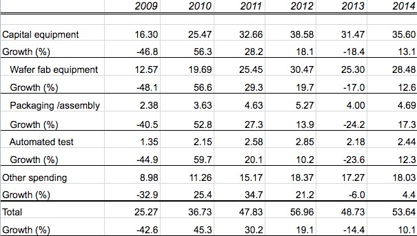
December 14, 2009 – The latest semiconductor capital spending forecast from Gartner solidifies the 2009 outlook with another positive bump-up, and the firm sees the climate significantly improving for almost all sectors well into the future.

The industry is enjoying "a very strong growth spurt" right now, noted Dean Freeman, research VP at Gartner. Foundries and a few memory companies started spending again in 2H09, and 1H10 will see an influx of technology upgrades; after a possible lull in 3Q10, look for capacity upgrades to ramp up into 2011s, he says.

After another dismal year in 2009 expanding on 2008’s dropoffs, every equipment sector will enjoy serious double-digit growth in 2010 — some above 50%, according to Gartner’s statistics. Wafer-fab equipment spending is seen surging nearly 57% (vs. a prediction of 38% just three months ago). The big question for this sector will be availability of 193nm immersion lithography tools, seen as critical for all technology upgrades — TSMC, for example, will be installing its first such tools, and leading-edge DRAM makers will move into the 4xnm range which also require the immersion tools. Gartner doesn’t predict a shortage yet, but long lead-times could limit WFE growth if demand continues to heat up.

Click to Enlarge
Worldwide semiconductor capital equipment spending forecast (US $B), 2009-2014. Some totals may differ due to rounding. (Source: Gartner)

Demand in the packaging/assembly sector will be overall very good (53% in 2010), but vary by certain equipment segments — e.g. advanced processes such as wafer-level packaging, 3D processes, and through-silicon vias (TSV), will require more investments going forward than the general market. Automated test equipment spending will surge nearly 60% in 2010, mainly due to the transition to mainstream adoption of DDR3 memory.

Another trend worth watching is industry consolidation, which has been seen in several examples following the past year’s meltdown and will likely continue, notes Gartner research VP Bob Johnson. "The impact of fewer equipment customers will continue to play out in the semiconductor equipment market and further consolidation is to be expected, with mergers and acquisitions, as well as companies closing down that can no longer afford to run a business in the semiconductor industry," he writes. "While initially this may seem to be a dark time for the equipment segment, as the industry consolidates a much stronger equipment sector will emerge to carry on in the future."

A few bits of explanation on the numbers (especially changes since the Sept. forecast), from Gartner’s Freeman, in an e-mail exchange with SST discussing the new numbers:

– A "rapid ramp" in 2H09 justified Gartner’s improved outlook for total capex in 2010 vs. its September outlook — but peeling the data into quarters, "you will find that growth is actually relatively flat coming off of 4Q09," Freeman noted. "2009 could see improved growth due to when revenue is taken/given by the equipment companies from the memory companies."

– Note that while outlooks have improved for almost every semiconductor equipment sector vs. Gartner’s September report, there is one exception:  automated test has had its outlook reduced not just for 2009 but the entire forecast period (see table below). "ATE spending declined mostly as a result that memory test has completely collapsed," and DDR3 ramps in 2009 "failed to materialize," Freeman explained. "The consolidation in the memory test space and improvement in test techniques will keep this growing at a lower pace than before."

– On the other hand, a substantial rise in "Other" capex, which is tied to buildings, software, etc., equates to a ramp in fab building, Freeman noted.

– Can we trust chipmakers — particularly historically gluttonous memory firms — to keep cool and not overheat the industry again, leading to more abrupt slowdowns and protracted downturns, as we’ve been predicting/hoping they would for years now? Memory badly overspent for capacity in the most recent cycle, creating a two-year downturn, Freeman noted, and it will once again build excess capacity — but this time "it will be a more muted cycle than previous ones," he predicts, which will narrow declining investments (and equipment sales) to just a single year instead of two deep years.

Click to Enlarge
Changes in Gartner’s forecasted semiconductor capital spending, Dec. 14 vs. Sept. 11.


December 8, 2009 – Researchers from Stanford U. have devised a way to turn ordinary paper into a battery: slather it with an inky concoction of carbon nanotubes and silver nanowires, and then cook it.

Coating a sheet of paper with ink containing carbon nanotubes and silver nanowires turns the paper into a "supercapacitor," which holds an electric charge like a battery but for a shorter period of time, and stores/discharges it much more rapidly. The particular version they came up with can last through 40,000 charge-discharge cycles, "at least an order of magnitude" better than conventional lithium-ion batteries, they claim. The thicker the coating, the greater the electrical storage/conductivity.

Yi Cui, assistant professor of materials science and engineering at Stanford, had previously done work on making such capacitive creations using plastics, but found the nanoink adheres better to the paper-based versions and makes them more durable; it can be folded and even soaked in acids or bases and performance does not degrade ("We haven’t tested what happens when you burn it," Cui quipped in a statement), and the CNTs resist peeling. No added adhesives also eliminates a factor that would otherwise decrease performance and increase production costs, the researchers note.

From their research, published this week by the Proceedings of the National Academy of Sciences:

Here, we show that commercially available paper can be made highly conductive with a sheet resistance as low as 1 ohm per square (Ω/sq) by using simple solution processes to achieve conformal coating of single-walled carbon nanotube (CNT) and silver nanowire films. […] When only CNT mass is considered, a specific capacitance of 200 F/g, a specific energy of 30-47 Watt-hour/kilogram (Wh/kg), a specific power of 200,000 W/kg, and a stable cycling life over 40,000 cycles are achieved. These values are much better than those of devices on other flat substrates, such as plastics. Even in a case in which the weight of all of the dead components is considered, a specific energy of 7.5 Wh/kg is achieved.

The main application for this work would be large-scale storage of electricity on the grid, in wind farms and solar energy systems. Other potential applications range from serving as the nonmetallic current collector in Li-ion batteries, to brushing onto a wall to create a conductive energy storage device to which LEDs could be connected, to use in electric or hybrid cars. "Society really needs a low-cost, high-performance energy storage device, such as batteries and simple supercapacitors," Cui said. "I don’t think it will be limited to just energy storage devices," noted Peidong Yang, professor of chemistry at the U. of California-Berkeley, quoted by Stanford. "This is potentially a very nice, low-cost, flexible electrode for any electrical device."

Click to Enlarge
SEM images of: (A) interface between carbon nanotubes and silver nanowires on Xerox paper, (B) Ag NW film, and (C) CNT film. (D) The resistance scaling with the Ag NW electrode distance. (Inset) Contact resistance measurement scheme. (Source: PNAS)


December 7, 2009 – Ten equipment and materials suppliers have received top nods from top foundry Taiwan Semiconductor Manufacturing Co. (TSMC) for contributions over the past year.

"We are very grateful for the full support of our suppliers during these challenging times for the global economy, and we hope to join hand in hand with them to overcome more challenges in the future through even stronger cooperation and closer partnership," said Stephen Tso, the foundry’s SVP and CIO, in a statement, adding a call to work closely with suppliers for other ends, e.g. solving "environmental problems" such as global warming and sustainability both environmental and industrial.

This year’s outstanding suppliers, praised by TSMC for "special contributions to delivery and technology cooperation during the economic downturn," include:

Equipment

– Best product: Ebara (CMP), Hitachi Kokusai Electric (furnaces)
– Best delivery support: Dainippon Screen (wet clean), Varian Semi. Equip. Assoc. (implanter)
– Best technology cooperation: ASML (lithography), Lam Research (etch)

Materials

– Supplier excellence awards: MEMC Electronic Materials (silicon wafers), Air Products and Chemicals (gas/chemical materials), Cabot Microelectronics (CMP materials), Tokyo Ohka Kogyo (lithography materials)

December 4, 2009 – After shrinking by nearly two-thirds over the past two years to lowest levels in more than two decades, global semiconductor equipment sales will surge mightily in 2010 and continue solid growth into 2011, according to updated forecast information from SEMI.

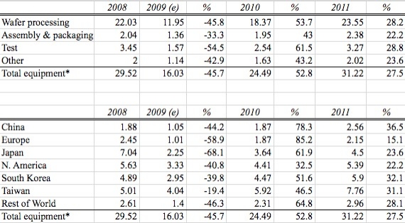
The new forecast pegs the final bloodbath of 2009: a -46% decline in total chip sales (33%-55% across individual segments) to $16.03B, the largest single-year decline since SEMI started tracking the numbers in 1991. That’s on top of a -31% decline suffered in 2008, to $29.52B.

But SEMI also projects an intense pickup in chip tool investments on the horizon: a 53% increase in 2010, and as much as 61% for backend application, driven by improved spending across memory (notably NAND flash), foundries, and packaging subcons, SEMI notes.
Click to Enlarge
Forecasts by equipment segment and region, in US $B. *Totals and percentages may differ due to rounding of numbers. (Source: SEMI)

By equipment segment, test equipment has taken the brunt of the 2009 downturn (-54%, to $1.57B), but will reap the most benefits in both 2010 (61%, to $2.54B) and 2011 (29%, to $3.27B). Assembly/packaging equipment is on the other end of the scale, suffering "only" a -33% decline in 2009 (to $1.36B), will keep to the curve in 2010 (43%, to $1.95B), and keep growing in 2011 but slightly less than other segments (22%, to $2.38B).

By region, 2009 was especially harsh to Japan (-68%) and Europe (-59%), but they will lead the march in 2010 with eye-popping growth (62% and 85%, respectively), alongside China (78%) and Rest-of-World (65%). China, ROW, and South Korea will lead in growth in 2011, each with >36% increases Y/Y.

Overall fab spending is expected to spike even more in 2010 (65%) — but with no new fabs are planned for the coming year, that raises the question about the industry’s preparedness to actually meet future demand, warns Christian Gregor Dieseldorff, with SEMI Industry Research and Statistics.

Click to Enlarge

Money spent on frontend facilities (R&D, pilot, volume fabs), in US $B. (Source: SEMI World Fab Forecast)

"Most companies will not invest in new facilities or significantly in new capacity in 2010," instead preferring to invest in technology upgrades, he writes in a new report. TSMC, Samsung, GlobalFoundries, and others are all in line to greatly increase spending, he notes. Construction spending is expected to surge 70% to $2.7B for an estimated 23 projects — but none of those are new facilities. A year ago SEMI’s World Fab Forecast projected 19 new fabs would start or resume in 2010; now, post-downturn, no additional plans are finalized, though five of those 19 are shells where delayed activity are expected to resume. In fact, 49 facilities have or will close by the end of 2010, which will reduce installed capacity by 4%-5%, a decline "unprecedented over the last 20 years" — even the post-2001 slump didn’t suffer a Y/Y decline, Dieseldorff notes.

In 2010, installed capacity is expected to put back 4%-5% installed capacity — but that means only returning to 2008 levels of demand. With utilization rates projected in the 80%-95% range (according to recent SICAS numbers), capacity sell-outs become a likelihood. Industry watchers now predicting anywhere from 10% to 22% semiconductor revenue growth in 2010. And with fabs investing in technology upgrades, not capacity, "the future growth rate of installed capacity appears not in sync with demand," he writes. It takes a year or more from groundbreaking to production ramp, so either capacity will be limited through 2010, or some devicemakers will realize they’ll be caught short and quickly start fab plans for extra capacity in 2011. And, he notes, "the one who is first, benefits the most."

December 3, 2009 – Researchers at the California Institute of Technology (Caltech) have combined the self-assembly ability of DNA with electronic properties of carbon nanotubes (CNT) to address the problem of organizing CNTs into nanoscale electronic circuits.

Click to Enlarge
(a) Single-wall carbon nanotubes labeled with "red" and "blue" DNA sequences attach to anti-red and anti-blue strands on a DNA origami, resulting in a self-assembled electronic switch. (b) An AFM image of one such structure. The blue nanotube appear brighter because it is on top of the origami; the red nanotube sits below. Scale bar is 50nm. (c) A diagrammatic view of the structure shown in b. The gray rectangle is the DNA origami. A self-assembled DNA ribbon attached to the origami improves structural stability and ease of handling. (Credit: Paul W.K. Rothemund, Hareem Maune, and Si-ping Han/Caltech/Nature Nanotechnology)

DNA origami is a type of self-assembled structure that can be programmed to form various shapes and patterns (e.g. smiley-faces, maps, even electrical diagrams). The structures are created from long single strands of viral DNA mixed with shorter synthetic DNA strands that bind them into desired shapes, generally 100nm on a side. Meanwhile, single-wall CNTs have intriguing electrical, strength, and heat conductive properties, but are problematic to arrange into desired patterns.

The solution they came up with was to soak the CNTs and DNA molecules in salt water, allowing the DNA to stick to the CNTs (protecting portions of them, to create a "handle" for recognition). Two batches were made ("blue" and "red"), and observed that single-strand DNA molecules with complementary sequences (e.g., "blue" and "antiblue") wrapped around to form a double helix. Next was building 100nm × 100nm "breadboards" in which DNA origami sequences are designed so that specific nanotubes will attach in preassigned positions — e.g., red-labeled CNTs crossing perpendicular to blue CNTs, to build a field-effect transistor (FET).

The systems were removed from solution and placed on a surface, and leads attached to measure electrical properties — and it indeed behaved like a FET, they claim. "One carbon, nanotube can switch the conductivity of the other due only to the electric field that forms when a voltage is applied to it," explained Paul W. K. Rothemund, Caltech senior research associate, in a statement. It didn’t work perfectly, noted Erik Winfree, Caltech associate professor of computer science, computation and neural systems, and bioengineering, but "it was sufficient to demonstrate the controlled construction of a simple device, a cross-junction of a pair of carbon nanotubes."

From their paper abstract:

We synthesize rectangular origami templates (75nm × 95nm) that display two lines of single-stranded DNA ‘hooks’ in a cross pattern with 6nm resolution. The perpendicular lines of hooks serve as sequence-specific binding sites for two types of nanotubes, each functionalized non-covalently with a distinct DNA linker molecule. The hook-binding domain of each linker is protected to ensure efficient hybridization. When origami templates and DNA-functionalized nanotubes are mixed, strand displacement-mediated deprotection and binding aligns the nanotubes into cross-junctions. Of several cross-junctions synthesized by this method, one demonstrated stable field-effect transistor-like behavior. In such organizations of electronic components, DNA origami serves as a programmable nanobreadboard; thus, DNA origami may allow the rapid prototyping of complex nanotube-based structures.

The group expects to improve their approach to more reliably build complex circuits involving not only CNTs but also other elements including electrodes and wiring. And the self-assembly approach is scalable to make multiple devices at a time, they note — e.g., enabling design of logic units for millions or billions of units self-assembling in parallel.

November 20, 2009 – The good news continues to shine in semiconductor equipment demand for suppliers in North America and Japan, according to the latest monthly data from SEMI and the SEAJ, though some softness may warrant some attention heading into the holiday season.

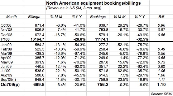
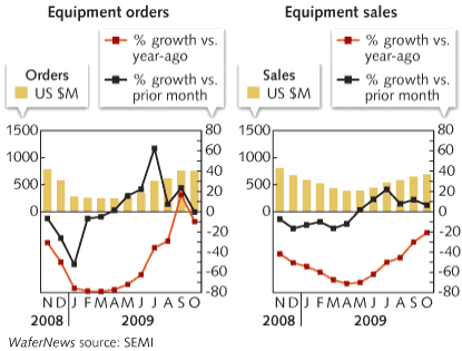
North America-based manufacturers of semiconductor manufacturing equipment received $756.2M worth of orders in October, about flat with September’s revised levels and just (barely) single-digit decline from a year ago. Billings also continued to improve Y/Y. now about -21% off, and still show M/M growth (though declining).

Japan, too, continues to see significant improvement in its chip tool sector, according to the Semiconductor Equipment Association of Japan (SEAJ). October bookings and billings (worldwide) were both up about 8% vs. September, to ¥66.42B and ¥48.22B, respectively, for a sparkling B:B of 1.28. It was the first Y/Y rise for global orders for Japan-made chip tools in 31 months, according to the SEAJ, though it cautioned against placing too much significance since the industry was well entrenched in its slump at this time a year ago.

Click to Enlarge

The good news, from SEMI’s numbers:

– Revised numbers for September were a little better than previously thought, about 3%-4% higher (bookings $758.9M vs. $732.8M, billings $648.4M vs. $624.6M), which translated into similar improvements in September’s M/M and Y/Y comparisons.

– The book-to-bill ratio (B:B) has stayed above the parity mark for four months now; October’s B:B of 1.10 means $110 worth of orders for every $100 worth of product billed for the month, a ratio that continues to indicate more business coming in than going out.

Things to watch:

– After finally showing sequential M/M growth to close the third quarter, bookings slipped back to a decline in October, a fact that bears watching, noted SEMI president/CEO Stanley Myers. He noted the group still continues to cautiously expect "slowly improving capital spending" for the rest of this year and into 2010.

– While suggesting an ongoing "slow" recovery, SEMI’s September revisions actually suggest the month was even more off-trend — nearly 17% M/M increase in orders and 12% in sales is well above previous months. With the holiday seasons coming up — and probably with extended downtime for suppliers still feeling pains from the downturn — it’s unlikely they’ll see business churn up again in the next couple of months.

Click to Enlarge