Category Archives: Materials and Equipment

by Michael A. Fury, Techcet GroupClick to Enlarge

April 28, 2011 – Day 4 of the MRS Spring 2011 meeting afforded me a bit more opportunity than yesterday to spend time outside of core CMOS issues. Screen printing with 80ft2 screens, for example, is pretty far afield from submicron fabrication methods. 3D integration was one focus for today, and there are a number of applications outside of electronics that are driving new printing and additive fabrication methods that may well serve the needs of the electronics industry.

Observation of the day: Session chairs come with a broad range of sensitivity to time and schedule. Flexibility and collegial discussions are welcome in single symposia, as they make good use of the extended knowledge and experience of people who have gathered from all over the world. But when the symposium is part of a 51-arm synchronized hydra, strict adherence to the printed schedule is a professional courtesy that needs to be uniformly respected.

MRS Spring 2011
Day 1: Lighting the paths for LED materials
Day 2: The III-V future of CMOS, the return of spin-on low-k
MRS Day 3: Memory, hardmasks, low-k — nothing’s confidential
Thin-film PV materials under the microscope @ MRS

(Additional presentation details can be found online on the MRS Spring 2011 abstracts page. The underscored codes at the beginning of papers reviewed below refer to the symposium, session, and paper number.)

Microdevices

Tsu-Jae King Liu of UC Berkeley (Q8.1) spoke about the use of NEMS devices for nonvolatile memory (NVRAM) applications, called NEMory. ION/IOFF and endurance for such devices are effectively ∞, with no radiation or shock sensitivity. By using an ONO charge trap nitride in the structure, the cantilever bias voltage can be adjusted to 0V, creating a bistable NV storage system with no power applied. Devices shown used an Al or TiN cantilever 0.1μm thick. Either the cantilever or the electrode must be coated with a thin oxide to avoid metal contact welding. In principle, the material set and fabrication methods are CMOS compatible and could be integrated into the on-chip interconnect levels. The ONO film only needs to be charged once, so a thick layer can be used, providing a 10-year retention time. Power consumption is two to six orders-of-magnitude lower than competing NVRAM technologies.

Virginia Chu from INESC Microsistemas e Nanotecnologias, Lisbon, Portugal (A13.1) talked about several applications of amorphous Si for the fabrication of MEMS and NEMS devices. Flex-mode resonators move out of plane and can suffer loss of Q in dissipative media, whereas bulk-mode resonators move in plane and can maintain a high Q in a variety of media. Bulk devices can also operate at a higher sustained resonance frequency. One device of interest is a magneto-resistive spin valve magnetic field detector that can sense deflections to 0.03Å optically and 0.06Å magnetically. Using flux concentrators, the device is being refined to sense the magnetic fields generated by human brain activity on the order of 10-12 Tesla (earth’s magnetic field is 10-4T).

Organic electronics

Stephen Forrest at the U. Michigan (T6.1) described the patterning of μm-scale organic electronics using organic vapor jet deposition. This is analogous to CVD TEOS vapor transport using a bubbler, except that in this method the organic source is deposited in its original form without decomposition. Patterning by shadow mask produces material gradients and poor edge definition that limit feature sizes to ~5μm. Nozzles are fabricated in Si with a resolution limit of printing 1.5μm features and a 30cm/sec substrate feed. It would take 25sec to print a 60" OLED display, but note that the method is more comparable to spray painting than to inkjet printing, as there is no on-off mechanism as presently implemented. Angstrom Engineering is their equipment development collaborator.

Tsuyoshi Sekitani from the U. of Tokyo (T6.2) showed some examples of large area (no, really large — 3.3m×3.5m screens!) screen printing of organic ICs with an accuracy of 20μm. On a smaller scale in their lab, they developed a new twill weave mesh material with high tensile strength (3000 N/mm) capable of tolerating very high viscosity silver inks that could deliver 25μΩcm resistivity with ambient temperature drying. This enabled formation of organic thin-film transistors with a 1mm cell pitch, not good enough for displays but adequate for sensors and other devices. Mobility was on the order of 0.1cm2/Vs. A PMOS unipolar inverter had a gain of 2, a CMOS circuit had a gain of 80. This screen print method was used to fabricate a flexible touch sensor sheet and a plastic mechanical switch array.

Extending the organic electronics themes from Forrest’s talk, Max Shtein at the U. of Michigan (T6.3) discussed the vapor jet printing of OLED and OPV materials. Among the objectives is the deposition of volatile organic materials without the use of solvents. Material flow is focused using a concentric guard flow of nitrogen or other low molecular weight gas. As guard flow rate increases, performance of Alq3, which is air and moisture sensitive, approaches that of vacuum-deposited material. Parylene CVD can be accomplished with the system by passing the precursor through a high temperature zone, which cracks the dimer to a monomer, then depositing the monomer on the substrate where it polymerizes.

Deposition

Francisco Zaera at UC Riverside (O7.5) studied the use of copper amidinate bis[(N,N’-di-sec-butylacetamidinate)Cu] as an ALD precursor. ALD monolayer behavior is observed at a deposition temperature of 350°K but at 400°K it is already behaving like CVD. A full monolayer of copper on a nickel substrate was achieved in 3-4 deposit/anneal cycles.

Avraham Rozenblat from Micron and Tel Aviv U. (O7.6) reviewed nucleation issues in the application of CVD tungsten below 45nm. Via shrinks decrease the bulk material and increase the interface contribution to via resistance. Over the deposition range of 290° C to 340° C on a Ti/TiN substrate, the resistance drop saturates at an average film thickness of 26nm regardless of temperature. Nucleation gives way to surface percolation conductivity before saturating with complete surface coverage.

Jon Gudmundsson at the U. of Iceland (O7.7) talked about the growth of ultra-thin TiN films on SiO2 using high-power impulse magnetron sputtering (HiPIMS), which produces crystallites smaller than DC magnetron sputtering but with a 30% lower deposition rate. On a MgO substrate compared to SiO2 substrate, the coalescence thickness drops from 1.09nm to 0.08nm, and the continuous film thickness drops from 5.5nm to 0.7nm. Films grown at 500°C are resistant to oxidation, indicating high density, and have a low resistivity of 54μΩcm on SiO2 and 16.6μΩcm on MgO.

Yair Ein-Eli at Technion-Israel Institute of Technology (O7.8) described a method for seedless electrodeposition of copper on Ta using an alkaline plating bath. It is expected to be applicable to Ru, Ru/Ta and other barrier metals that form a native oxide. Electrochemical studies were carried out in a K4P2O7 medium (pH 9.3). Native Ta2O5 oxide was first electrochemically reduced to metal, then copper solution with 3ppm DMcT were added and the potential was moved from -2V to -1.2V for deposition.

Cu TSVs, packaging tests, 3D interconnects

Arif Budiman from LANL (O8.3) studied mechanical stresses in copper through-silicon vias (TSV) using in situ synchrotron X-ray submicron diffraction. Grain size and stress mapping of the Cu within the via and of the Si itself during the post-deposition anneal proved itself to be a useful tool for understanding the mechanism behind via popping. All you need is a synchrotron.

Hae-A-Seul Shin of Seoul National U. (O8.4) talked about the evolution of damage during thermal cycling of Cu TSV studied with FIB, EBSD, and synchrotron XRD (yes, she used the same synchrotron in Berkeley as in the study above). Grain structure was found to be stable for 1 year following a 200°C anneal, thought to be due to the abundant presence of twin grain boundaries. Annealing reduced the average hydrostatic stress in the Cu from 229MPa to 177MPa due to the formation of voids and cracks.

Alexander Hsing at Stanford (O8.2) demonstrated the use of a suite of microprobe test methods for compressive, tensile and shear loading capabilities of Pb-free solders and structures used in chip bumps, pads and other electronic packaging schemes. The metrology operates at nanoscale dimensions lower than that used in conventional techniques.

Xiaopeng Xu from Synopsys (O8.5) described a simulation test method for evaluating stresses in microbump and underfill systems for a range of bump diameters, underfill materials, and geometry layouts. The effects of process sequence and annealing profiles were examined. It was observed that the chip regions with the largest device performance variation are not necessarily the same as the regions where the structure reliability is a greatest risk.

Owen Hildreth at Georgia Tech (O8.6) introduced metal assisted chemical etching (MaCE) for use in 3D interconnects. The metal catalyst moves into the Si substrate with the etch front, preserving the profile with etch depth. A shaped catalyst can create features not possible with other methods; for instance, an asymmetric catalyst will rotate as the etching proceeds, producing a hole with sidewall threads, like a screw. Such a via hole would provide mechanical adhesion for a TSV rather than relying only on interfacial adhesion.

Nanostructures and nanoparticles

Marco Rolandi of the U. of Washington (T7.6) talked about direct write of Si, Ge, and SiGe nanostructures using a biased AFM tip, a form of dip-pen nanolithography, an interesting technique with limited application in the manufacturing world. Productivity was increased by using a patterned gold-coated PDMS stamp. The ink was diphenyl silane or germane. Characterization of the deposited material showed high quality, carbon-free material by SIMS and X-ray PEEM. A roadmap for further improvement of the technique was shown.

Eric Duoss of the U. of Illinois @ Urbana (T7.7) taught us about direct-write assembly of functional inks for conductive microstructures. Today’s lesson covered a silver nanoparticle ink fabricated with a 20nm average particle size with a range of 5nm-50nm. Control of the ink velocity permits conformal printing or true 3D printing. Using up to a dozen passes, 3D features with an aspect ratio of 7 can be fabricated. Stacked chip joining was demonstrated by printing across an air bridge between the chip and the substrate below. This is possible because the ink dries so quickly as it exist the nozzle, making it, in effect, a fluid bonding wire that is available on demand. Conformal printing on hemispherical surfaces can be used to fabricate low Q antennas for mobile communications devices.

Printed electronics

Romain Cauchois from Gemalto (France) (O8.9) tailored the crystallographic texture and electrical properties of inkjet printed interconnects to optimize performance for RF and related applications. Their system operates with 30pL drops of a commercial silver ink with 30-40nm particles. Sintering is accomplished at 200°C using a rapid ramp of 150° C/min. Silver grain growth was also augmented by depositing a thin gold layer before the silver features, which resulted in a fiber texture that was not otherwise achievable. The resulting structure proved to improve wire bonding results over the conventional process.

PV

Bill Nemeth of NREL (A16.5) talked about use of a light down shifting (LDS) thin-film coating to improve the performance of a-Si:H solar cells. The concept is to use the wasted light that is not otherwise absorbed by the cell by shifting the frequency of the light that falls outside of the cell’s peak absorption range. Down shifting differs from down conversion in that shifting implies a conversion efficiency <100%. Instead of the expected current gain of 0.28mA/cm2, they saw a loss of 0.13mA/cm2. This was attributed to side scattering due to nonoptimized experimental conditions. They will try again.


Michael A. Fury, Ph.D, is senior technology analyst at Techcet Group, LLC, P.O. Box 29, Del Mar, CA 92014; e-mail [email protected].

April 28, 2011 — SEMI, the global industry association serving the manufacturing supply chain for the microelectronics, display, photovoltaic and related industries, announced that president and CEO Stanley T. Myers has informed the SEMI International Board of Directors of his intention to step back from executive leadership of SEMI this year.

Myers has participated for more than 50 years in the semiconductor industry, including 24 years as a SEMI board member and 15 years as president and CEO of the association. He was chairman of the SEMI International Board in 1994.

Last year, the Semiconductor Industry Association (SIA) also changed leadership, with Brian C. Toohey taking over the president role from George Scalise, who has led the association since 1997. Prior to joining SIA, Toohey served as senior vice president of the Pharmaceutical Research and Manufacturers of America (PhRMA). He has also held senior management positions at DEKA R&D Corporation, AirCell, Inc., and the U.S. Department of Commerce.

SEMI Board of Directors Chairman Rick Wallace (CEO of KLA-Tencor) has appointed a Board search committee to evaluate candidate successors for the role that Myers will be vacating. Tim O’Shea, with the executive search firm Heidrick & Struggles, will conduct the search for SEMI. Myers plans to continue supporting the association when a new president and CEO is named.

"Under [Myers’] leadership, SEMI has grown and diversified to meet the changing needs of member companies that participate in one of the world’s most complex and sophisticated high-tech industries. As Stan anticipates the next chapter of his life, we appreciate his thoughtful and deliberate framework for a succession plan."

Prior to his appointment as SEMI president and CEO, Myers worked for 17 years at Siltec where he served as president and CEO until 1985. In 1986, Siltec was acquired by Mitsubishi Materials Corporation. Siltec changed its name to Mitsubishi Silicon America (MSA) and Myers continued as president and CEO until he moved to SEMI in 1996. Prior to Siltec/MSA, Myers worked for Monsanto Corporation for 18 years.

Myers is chairman of the National Science Foundation (NSF) Advisory Board to MATEC (Maricopa Advanced Technology Education Center). He also is a member of the Engineering Advisory Board to the School of Engineering, San Jose State University.

Myers was the recipient of the Exemplary Community Leadership Award by the Silicon Valley Conference on Community and Justice in 2006. In May 2007, he was inducted into the Chemical and Petroleum Engineering Hall of Fame at the University of Kansas. In February 2008, Myers was inducted into the Silicon Valley Engineering Hall of Fame.

SEMI is the global industry association serving the manufacturing supply chains for the microelectronic, display and photovoltaic industries. For more information, visit www.semi.org.

Subscribe to Solid State Technology/Advanced Packaging.

Follow Solid State Technology on Twitter.com via editors Pete Singer, twitter.com/PetesTweetsPW and Debra Vogler, twitter.com/dvogler_PV_semi.

Or join our Facebook group

April 28, 2011 – BUSINESS WIRE — Tokyo-based JSR Corporation named the first non-Japanese Officer to its Officers Committee. Eric R. Johnson, the current president of the company’s US semiconductor materials operations, JSR Micro, Inc., has been named as an Officer effective June 17.

While JSR has always functioned internationally, Johnson’s placement on the Officers Committee is representative of the company’s push to make JSR a truly global company, internally and externally, and of the critical role JSR Micro, Inc. (the US operations) is expected to play in the strategic future of the company. "For the JSR Group, North America is a strategically crucial market where we are expanding our businesses beyond semiconductor materials," said Mitsunobu Koshiba, president of JSR Corporation.

Johnson joined JSR Micro in 2001 as a senior vice president and was named president in 2005. As an Officer, Johnson will continue in his role as president of JSR Micro, Inc. but will also be involved in strategic planning and the strategic review process for JSR Corporation.

Johnson called the appointment a "tremendous honor" and stated his desire to support JSR’s strategic vision and people globally.

JSR Corporation is an advanced manufacturer in high-performance chemicals. JSR operates a wide array of global businesses ranging from the petrochemical business, including synthetic rubber, to the cutting-edge information processing and electronic materials business, including the manufacture of semiconductor materials and liquid crystal display materials.

JSR Micro supplies electronic materials to the world’s leading semiconductor manufacturers for imaging, packaging and CMP applications. Learn more about JSR Micro at http://www.jsrmicro.com/

Subscribe to Solid State Technology/Advanced Packaging.

Follow Advanced Packaging on Twitter.com by clicking www.twitter.com/advpackaging. Or join our Facebook group

By Debra Vogler, senior technical editor

April 25, 2011 — Imec researchers will present a paper titled "Carbon nanotube interconnects: electrical characterization of 150nm CNT contacts with Cu damascene top contact" at the IITC 2011 Conference (May 9-12, Dresden, Germany).

Click to EnlargeDr. Marleen van der Veen, senior research scientist at imec discussed the research results and their significance in this podcast interview:  Download or Play Now
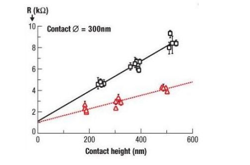
Van der Veen highlighted the process technologies and steps used to grow the carbon nanotubes (CNTs) and the properties and attributes of the multi-walled CNTs (MWCNT) that resulted (Fig. 1). As noted in the paper, the lower slope for the Al2O3 pre-coated CNT implies a three times better CNT resistivity than the SiO2-coated ones.

Click to Enlarge

Figure 1. Single CNT contact hole resistance as a function of the contact height for CNT coated with SiO2 (solid line) and Al2O3/SiO2 (dotted line).

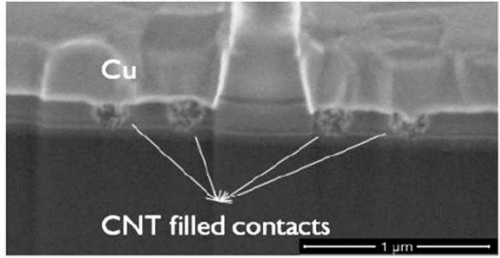
The researchers took the integration process for 300mm contacts and transferred it to 150nm contact holes compatible with the module for 130nm device technologies (Fig. 2). The researchers maintain that because CNTs grown from different recipes and processed under different conditions can be rapidly benchmarked, they believe that their work will be important for manufacturing CMOS-compatible CNT interconnects, as well as for improving CNT interconnect resistance in advanced CMOS interconnects.

a) Click to Enlarge
b) Click to Enlarge

Figure 2. SEM images from different stages of the integration in 150nm contact holes a) before damascene litho and b) after barrier deposition and Cu fill.


More IITC previews:

IBM IITC preview: BEOL interconnect tech for <22nm

Beyond ball shear test: Microprobing chip/package stress at Stanford

By Debra Vogler, senior technical editor

April 25, 2011 — Imec researchers will present a paper titled "Carbon nanotube interconnects: electrical characterization of 150nm CNT contacts with Cu damascene top contact" at the IITC 2011 Conference (May 9-12, Dresden, Germany).

Click to EnlargeDr. Marleen van der Veen, senior research scientist at imec discussed the research results and their significance in this podcast interview:  Download or Play Now
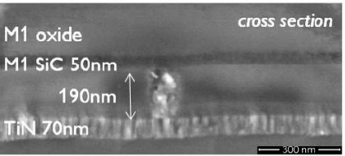
Van der Veen highlighted the process technologies and steps used to grow the carbon nanotubes (CNTs) and the properties and attributes of the multi-walled CNTs (MWCNT) that resulted (Fig. 1). As noted in the paper, the lower slope for the Al2O3 pre-coated CNT implies a three times better CNT resistivity than the SiO2-coated ones.

Figure 1. Single CNT contact hole resistance as a function of the contact height for CNT coated with SiO2 (solid line) and Al2O3/SiO2 (dotted line).

The researchers took the integration process for 300mm contacts and transferred it to 150nm contact holes compatible with the module for 130nm device technologies (Fig. 2). The researchers maintain that because CNTs grown from different recipes and processed under different conditions can be rapidly benchmarked, they believe that their work will be important for manufacturing CMOS-compatible CNT interconnects, as well as for improving CNT interconnect resistance in advanced CMOS interconnects.

a) 
b) 

Figure 2. SEM images from different stages of the integration in 150nm contact holes a) before damascene litho and b) after barrier deposition and Cu fill.


More IITC previews:

IBM IITC preview: BEOL interconnect tech for <22nm

Beyond ball shear test: Microprobing chip/package stress at Stanford

by James Montgomery, news editor

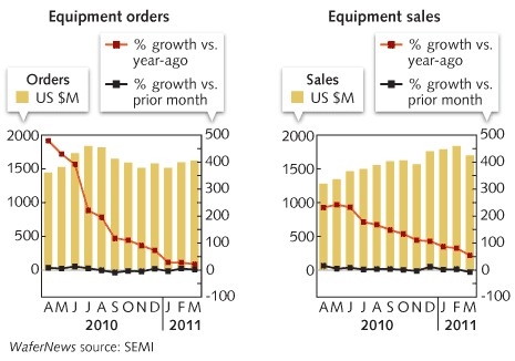
April 25, 2011 – Demand for semiconductor manufacturing equipment climbed again in March to a six-month high, according to data from SEMI.

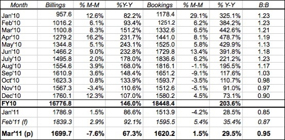
For March, North America-based manufacturers of semiconductor equipment posted $1.62B in bookings, up 1.5% from February and 21% higher than a year ago. Billings were just a fraction under $1.70B, a -7.6% sequential decline but still up 50% Y/Y. Compared with preliminary results, SEMI added about $11M-$2M to February’s totals for both sales and bookings.

Preliminary 1Q11 data indicates a 7.6% increase in sales ($5.326B) vs. a 0.9% increase in bookings ($4.730B).

Click to Enlarge

Click to Enlarge

A look inside the March 2011 numbers:

  • Bookings have added about $100M in the past two months — for most firms it’s the close of their 1Q11 books. But overall the total bookings hasn’t fluctuated much beyond the $1.5B-$1.6B range since Sept. 2010. "We see industry investments remaining steady," noted SEMI president/CEO Stanley Myers, in a statement.
  • The billings data is a little curious. Usually sales get a bump in a fiscal/calendar quarter-ending month — but in March they gave back $140M, more than half the $260M that had been added in the previous three months. It’s likely just the passing of a bubble down the supply chain — tool bookings took a -9% hit back in September, implying a reasonable six-month fulfillment pipeline.
  • The book-to-bill ratio climbed again to 0.95, meaning $95 worth of orders received for every $100 billed. That means more business is going out (sales) than coming in (orders), but it’s also within shouting distance of the 1.0 parity mark, and is closer than the three previous months.

In Japan, more sales than bookings were tallied during March — ¥122.037B/US $1.49B (+20.9% M/M), vs. ¥115.862B/$1.90B (+5%) — so the B:B ratio slipped below parity to 0.95.

Breaking the backend-frontend trend correlation

While SEMI’s monthly numbers are really a trailing indicator of industry health, they can provide some insight into specific sectors’ performance and what might be expected next. Frontend bookings in March (the 3-mo. average) were $1.37B, down -0.7% M/M and -1.4% Q/Q — but backend tool bookings spiked 22.6% M/M (32% Q/Q) to $246M, points out Satya Kumar from Credit Suisse in a research note. Backend billings grew 19.5% M/M to $244.9M, resulting in an above-parity B:B of 1.01, better than the overall market.

The March data also is noteworthy because they encompass three weeks of post-quake data out of Japan, Kumar notes.

The aforementioned plateau in equipment bookings supports Kumar’s assertion that we’re in a period where the industry’s typical peaks and valleys are being muted somewhat, and there’s no longer a clear pathway between backend (leading) and frontend (trailing) cyclicality. Kumar brackets this particular cycle we’re in at ~2009 trough – 2013 peak; initially bookings rose as utilization levels pick up, but by now they’re being "sustained at high levels such that supply additions roughly equal demand growth," he writes. Backend bookings, meanwhile, "have gone through a full cycle," peaking last July, troughing in November, and now up 36% from then, "all the while frontend bookings were either increasing or have been sustained at high levels." So, last year’s backend bookings drop didn’t correlate to frontend declines as might have been expected, he writes. "Instead, equipment lead time differences for the segments, time taken to add new capacity, and overall supply/demand for the two segments are the drivers for orders."

April 25, 2011 — A University of Arkansas physicist has received the largest award granted to an individual researcher from the Army Research Laboratory to search for a novel class of nanomaterials with rationally designed properties.

Physicist Jak Chakhalian seeks to create a new class of materials: topological insulators combined with magnetic and superconductivity properties within just a few atomic layers. The materials could enable topological quantum computers, which could break complex encryption codes and compute things beyond the power of today’s supercomputers.

"It will revolutionize the way we think about electrons moving in conventional insulators and metals even at the nanoscale," Chakhalian said. The Army Research Lab is funding his research with $1.2 million over five years.

Recently Chakhalian, associate professor of physics in the J. William Fulbright College of Arts and Sciences, and colleagues found that atomic orbitals change substantially at the interface between a ferromagnet and a high-temperature superconductor. This finding opens up a new way of designing nanoscale superconducting materials. It also fundamentally changes scientific convention, which suggests that only electron spin and atomic charge — not atomic orbitals — influence the properties of nanostructures.

Chakhalian wants to create a topological insulator as a nanostructure with magnetic and superconducting properties in a few atomic layers at the interface.

Chakhalian will use the grant from the Army Research Laboratory to build new equipment to create and test atomically thin superlattices by combining novel materials and using the interface as a tool.

Photo. Doctoral student Benjamin Gray, left, and Jak Chakhalian in the laboratory with a unique state-of-the-art piece of equipment built last summer to fabricate atomic layers of complex oxides.

This research was cited by Science as one of the top 10 research breakthroughs of 2007.

Until recently, researchers only recognized three fundamental types of materials: metals such as iron and gold, insulators and semiconductors. In 2006, theoretical physicists suggested that another completely unknown class of insulating materials might exist. This class, called topological insulators, would not conduct electricity inside the crystal but permits the perfect conduction on the surface within a single atomic layer. This happens because geometry protects the surface electrons. In 2007, scientists looked at the alloy bismuth telluride and found the properties that this theory predicted. They had discovered a new class of material.

"On the inside, bismuth telluride is an insulator, but on the surface, within one atomic layer, it’s a perfect conductor," Chakhalian said. "It will conduct within the single atomic layer no matter how disordered the crystal on the inside. This is a whole new class of materials very similar to the Nobel prize-winning material, graphene, with many other interesting twists."

Chakhalian is a member of the University of Arkansas Institute for Nanoscience and Engineering. He holds the Charles E. and Clydene Scharlau Endowed Professorship in Chemistry.

Learn more at http://www.uark.edu/home/

Follow Small Times on Twitter.com by clicking www.twitter.com/smalltimes. Or join our Facebook group

April 23, 2011 — North America-based manufacturers of semiconductor equipment posted $1.70 billion in orders in March 2011 (three-month average basis) and a book-to-bill ratio of 0.95, according to the March Book-to-Bill Report published by SEMI.

The three-month average of worldwide bookings in March 2011 was $1.62 billion. The bookings figure is 1.5% more than the final February 2011 level of $1.60 billion, and is 21.6% above the $1.33 billion in orders posted in March 2010.

The three-month average of worldwide billings in March 2011 was $1.70 billion. The billings figure is 7.6% less than the final February 2011 level of $1.84 billion, and is 54.4% more than the March 2010 billings level of $1.10 billion.

"Orders are over 20% higher than one year ago and we see industry investments remaining steady," said Stanley T. Myers, president and CEO of SEMI. 

  Billings (3-mo. avg)  Bookings (3-mo. avg) Book-to-Bill
October 2010 1,623.3 1,593.7  0.98
November 2010  1,567.3 1,512.6 0.97
December 2010   1,760.1  1,580.2 0.90
January 2011  1,786.9  1,513.9 0.85
February 2011 (final)  1,839.3  1,595.5 0.87
March 2011 (prelim)  1,699.7  1,620.2 0.95
Billings and bookings figures are in millions of U.S. dollars. Source: SEMI April 2011.

The SEMI book-to-bill is a ratio of three-month moving averages of worldwide bookings and billings for North American-based semiconductor equipment manufacturers. A book-to-bill of 0.95 means that $95 worth of orders were received for every $100 of product billed for the month.   

The data contained in this release were compiled by David Powell, Inc., an independent financial services firm, without audit, from data submitted directly by the participants. SEMI and David Powell, Inc. assume no responsibility for the accuracy of the underlying data.

The data are contained in a monthly Book-to-Bill Report published by SEMI. The report tracks billings and bookings worldwide of North American-headquartered manufacturers of equipment used to manufacture semiconductor devices, not billings and bookings of the chips themselves. The Book-to-Bill report is one of three reports included with the Equipment Market Data Subscription (EMDS).

SEMI is the global industry association serving the manufacturing supply chains for the microelectronic, display and photovoltaic industries. For more information, visit www.semi.org. Read SEMI’s blog.

Subscribe to Solid State Technology/Advanced Packaging.

Follow Solid State Technology on Twitter.com via editors Pete Singer, twitter.com/PetesTweetsPW and Debra Vogler, twitter.com/dvogler_PV_semi.

Or join our Facebook group

April 23, 2011 — Laird Technologies Inc. released the Tpcm 580SP Series phase change material, a high-performance, screen-printable or stencilable thermal interface material (TIM) product with a thermal conductivity of 4.0W/mK that provides an alternative to thermal grease.

The PCM pad contains a solvent that assists in processing, which allows for surface wetting. After drying, the solvent is moistureless to the touch, and therefore eliminates the mess associated with thermal grease.

Once the solvent is removed, Tpcm 580SP begins to soften and flow at temperatures around 45

April 20, 2011 – Intel has handed out its annual supplier awards, this year to 28 companies, including some one-time "Achievement" awards for particular impact.

Click to Enlarge
(Image of statue from Intel.com)

To earn Intel’s "Supplier Continuous Quality Improvement" (SCQI) award — now in its 24th year — eight companies (vs. 10 honorees in 2009 and 16 in 2008) scored at least 95% on a list of performance and ability goals, including cost, quality, availability, delivery, technology and environmental/social/governance, over the past year. They also achieved ≥90% on an improvement plan and "demonstrated solid quality and business systems."

Another 20 suppliers (vs. 16 in 2009 and 26 in 2008) scored 80% or better to earn Intel’s 2010 "Preferred Quality Supplier" (PQS) recognition. Criteria include "consistently exceed[ing]" Intel expectations, aligning to technology and manufacturing roadmaps, meeting cost reduction goals, and delivering excellent "customer satisfaction." And this year, four suppliers were picked for an "Achievement Award," billed as a "one-time extraordinary achievement" that has "enabled significant business impact to Intel across the areas of cost, quality, availability, technology, sustainability and customer satisfaction."

"Our industry is experiencing significant changes that make it even more important to partner with outstanding suppliers to deliver leading-edge technology to our customers," noted said William Holt, SVP/GM of Intel’s Technology and Manufacturing Group, in a statement. "Continuous improvement is what differentiates good companies from great companies," added Brian Krzanich, SVP/GM of Intel’s Manufacturing and Supply Chain, and the eight SCQI winners excelled in "innovation, agility, customer responsiveness, and environmental sustainability."

More facts about this year’s inductees:

  • Disco, Hitachi High-Tech, Hitachi Kokusai, Senju, and Sumco are all threepeat SCQI winners. Fujifilm and Rofin-Baasel are three-time PQS winners.
  • TEL was the only supplier to climb up from last year’s PQS ranks into SCQI status.
  • Falling off last year’s SCQI list from a year ago: Daewon Semiconductor Packaging (now PQS status), DEK, Moses Lake/Tama Chemicals (also PQS status), Munters, and Verizon.
  • Gone from the PQS list: AceCo, ASE, Cisco, Nippon Mining & Metals, Nordson ASYMTEK, and Praxair Electronics. Grohmann and Hirata were PQS winners in 2009 but took home this year’s inaugural "achievement award."
  • Note that ASML and Nikon are both are still among Intel’s most recognized suppliers. Nikon used to be the incumbent litho tool supplier (and SCQI winner in 2008), but Intel is known to be splitting its litho business now with ASML — and with both suppliers recognized for a second year in a row, that plan seems to be working well.

Intel launched the SCQI program in 1987 to improve the systems and output of key suppliers, and minimize its time and money spent inspecting incoming material, goods, and services purchased. The company honored 26 companies in 2009, 40 in 2008, 48 in 2007, 54 in 2006, 38 in 2005, 43 in 2004, 45 in 2003, and 42 in 2002. (Note the trend of fewer companies being honored; the company didn’t say whether this is attributable to its own criteria, or to marketplace dynamics.)

The 2010 SCQI winners are:

* Disco (blade dicing and laser saws, wafer thinning, and polishing equipment)
* Hitachi High-Technologies (etching systems, FE-SEMs, CD-SEM, defect inspection tools)
* Hitachi Kokusai Electric (diffusion furnaces)
JSR (photoresists, packaging materials, and CMP consumables)
* Senju Metal Industry (electronic interconnect materials)
Shinko Electric Industries (plastic laminated packages and heat spreaders)
* SUMCO (200mm and 300mm polished and test silicon wafers)
** Tokyo Electron (semiconductor production equipment)

Winners of the 2010 PQS award include:

** ASML (lithography process tools)
** Cabot Microelectronics (CMP slurries)
* Daewon Semiconductor Packaging (handling media)
** Daifuku (fab automated material handling systems)
Dai Nippon Printing (advanced photomasks)
** Fujifilm Electronic Materials (chemistry, equipment for semiconductor device manufacturing)
Mitsubishi Gas Chemical (chemicals for semiconductor device manufacturing)
* Moses Lake Industries/TAMA Chemicals (ultrahigh-purity chemicals)
Murata Manufacturing (multilayer ceramic capacitors, inductors, and interference components)
** Nikon (lithography scanners and steppers)
** Rofin-Baasel (laser mark equipment)
Siltronic (polished and epitaxial silicon wafers)
STATS ChipPAC (turnkey packaging and test services)
Taiyo Yuden (multilayer ceramic capacitors, inductors, electromagnetic interference components)
TSMC (foundry services)

And the four suppliers named for one-time "achievement award" are:

Advantest (test equipment), for "velocity and availability"
Gemteck Technology (wireless products), for "customer satisfaction"
** Grohmann Engineering (assembly equipment), for "affordability"
** Hirata (automation equipment), for "breakthrough technology"

(* a 2009 SQCI winner)
(** a 2009 PQS winner)