Category Archives: Metrology

July 13, 2011 — At SEMICON West 2011, Phil Bryson, SEMATECH, covers the top challenges in semiconductor metrology at advanced nodes.

FINFet metrology, defect inspection at design rule size, EUV mask defects are on his mind.

Right now, SEMATECH is zeroing in on legacy and replacement techniques — which can be continued to enable high-volume manufacturing, and which need to make the transition to new processes.

Subscribe to Solid State Technology/Advanced Packaging.

Follow Solid State Technology on Twitter.com via editors Pete Singer, twitter.com/PetesTweetsPW and Debra Vogler, twitter.com/dvogler_PV_semi.

Or join our Facebook group

July 13, 2011 – ASML has added three extensions to its Twinscan NXT 1950i immersion lithography tool, to improve imaging, overlay, and system throughput.

Just as the company’s FlexRay freeform illumination system (released at SEMICON West in 2009) offers better tuning of the source, so a new FlexWave technology allows application-specific wavefront correction within the lens, offering control to reduce both aberration fingerprint of the projection optics and lens heating effects.

Also, to compensate for reticle heating typically found in high dose layers with low transmission reticles, a new Reticle Control technology incorporates a sensor to measure reticle temperature profile through the first production lot, then predict thermal expansion per exposure, and calculate feed-forward corrections to lens and stage parameters.

Thirdly, ASML is offering a "performance enhancement package" (PEP) of hardware and software upgrades — faster metrology cycle, stiffer position module, and immersion hood to improve dynamic and thermal behaviors for faster speed scans — that it says improves throughput from 175 wafers/hour to 200 WPH at 125 shots, and up to 230 WPH at 96 shots.

All are available as field upgrades, and are available now or will be later this quarter.

July 12, 2011 — Olympus Integrated Technologies America launched the latest 3DIR Metrology and Defect Review System at SEMICON West 2011, booth 1524. The system uses a confocal IR laser scanning microscopy technology for measuring post bond parameters of three dimensional stacked integrated circuits (3DS-ICs).

Greg Baker, president and COO of Olympus Integrated Technologies America, discusses why the company chose to focus its efforts on infrared (IR) metrology for defect inspection of bonded wafers.


The company uses IR because silicon is transparent to near-IR wavelengths. IR microscopy enables acquiring very high resolution, clear images; the key to such images is the laser scanning confocal capability of the microscope — it eliminates out-of-focus layers that are reflected back from the sample, explains Baker. 

Olympus’ 3DIR metrology system measures alignment points at selected die of bonded wafers, stores images and data, and summarizes results. Correlation of overlay alignment offset data to electrical yield provides an early indication of bonded wafer yield. Software tools are provided to display data in the form of vector maps for further review and analysis.

Figure. A pre-bond particle defect is imaged in visible light. Then relocated and imaged using IR microscopy after wafer bonding. The bonding process has compressed and enlarged the defect to short two lines.

The company integrated the laser confocal microscope into the fully automated metrology tool in partnership with SEMATECH. Three applications that are capable with the resulting tool are: 1) overlay alignment measurements; 2) 3D reconstructions; and 3) defect review (see the figure).

The confocal capability of the microscope allows thin optical sectioning in Z and construction of 3D images of the bonded wafer interface and structures. The 3D reconstructions can be used to create sections in the XZ plane to provide a measurable profile of an imaged structure or feature. Using the confocal capability of the microscope to take XZ measurements at various points on the wafer provides information on the bond interface thickness uniformity.

Using the system’s IR microscope imaging capability, bonded wafers are automatically scanned at low magnification. Images are stitched together to form a single wafer image. When the overlay vector map is superimposed on the scanned wafer image, correlation of many of the failed overlay measurement points to bonded interface anomalies can be seen. Because the wafer scan is done using an IR microscope, the stitched image can be viewed and zoomed for more detail. In addition, any site can be revisited and the image reviewed or rescanned and imaged using the IR microscope with objective magnifications up to 90X and 0.14

July 11, 2011 – PRNewswire — EV Group (EVG), MEMS, nanotechnology and semiconductor manufacturing tool supplier, released a wafer bonding system for 450mm silicon-on-insulator (SOI) wafers: EVG850SOI/450-mm. The automated tool runs at production line speed and comprises a cleaning module and pre-bonding module.

The EVG850SOI/450-mm cleaning module cleans and pre-conditions wafers before wafer bonding. In the pre-bonding module, the two silicon wafers are joined together either in a vacuum or in an atmospheric chamber. 450mm load ports and front opening unified pods (FOUPs) complete the tool.

Most of the particle and metal ion contamination tests will be performed on 300mm wafers due to the lack of 450mm metrology systems.

SOI wafer provider Soitec will install, test and qualify the first EVG850SOI/450-mm system at its Grenoble, France, headquarters in Fall 2011. Soitec’s Smart Cut layer transfer technology is "one of the most important SOI fabrication processes based on wafer bonding," said Paul Lindner, EV Group Executive Technology Director.

Tool development was done in cooperation with the European Semiconductor Equipment and Materials Initiative. In this interview, Lindner discusses the challenges of designing for 450mm as well as SOI: cleanliness issues and the impact of the much larger mechanical components that come into contact with the wafers.

"The bonding step acts like a magnifying glass for particles, so anything trapped at the bond interface is a problem and needs to be eliminated," explained Linder. "So in the tool, particle control is the biggest challenge for SOI wafers."

EVG points out that SOI will enable better power/performance for sub-22nm node CMOS and 3DICs compared to similar-geometry bulk CMOS. Wafer bonding allows chip makers to acheive high-quality, single-crystal Si films on one insulating layer, making a SOI substrate. Though SOI has not yet been adopted by all the major players, EVG’s customers say that they expect that sometime below 22nm, or maybe even at 16nm, the use of an engineered substrate (not necessarily SOI) will be much more attractive. Looking ahead to the insertion point for EVG’s first 450mm wafer bonding system, Linder’s forecast — probably at 16nm — occurs about the time when engineered substrates (whether SOI, or GOI, or some other layer-transferred substrate) become more heavily adopted is as follows: 1) installation of the first tool in 2011, 2) obtain the first bonded wafers in 2011, 3) enter pilot line production by 2014, and 4) achieve production at end users by 2016.  

The tool can be used to fab 300mm wafers as facilities transition from 300 to 450mm.

The tool is EVG’s first for 450mm wafers, and will serve as a blueprint for future systems, both for wafer bonding and lithography, EVG reports. An extension of the system with additional modules is planned as a further step to increase wafer throughput.

Learn more about the new tool at SEMICON West booth 1131 this week, Moscone Center in San Francisco, CA.

EVG’s Paul Lindner will be part of the MCA’s BrightSpots Forum on 450mm, Monday at 6:00PM during SEMICON West. To register for online access to the live panel event, click here: https://www2.gotomeeting.com/register/378232715.

EV Group (EVG) makes wafer-processing solutions for semiconductor, MEMS and nanotechnology applications. More information is available at www.EVGroup.com.

Subscribe to Solid State Technology/Advanced Packaging.

Follow Solid State Technology on Twitter.com via editors Pete Singer, twitter.com/PetesTweetsPW and Debra Vogler, twitter.com/dvogler_PV_semi.

Or join our Facebook group

July 11, 2011 — Jan Vardaman, president and founder of TechSearch International, summarizes highlights from her SEMICON West presentation on through silicon vias (TSV) (Tuesday, July 12, 2:00-4:30PM,  Heterogeneous Integration session). "We’re finally moving from PowerPoint engineering to real engineering [with respect to TSVs,]" said Vardaman, though progress is slow and will require patience. Wafer bond/debond and wafer thinning/wafer handling are gaining the most attention, she says. And supply chain logistics responsibilities (foundries vs. outsourced semiconductor assembly and test [OSAT]) need to be worked out. Metrology tools are needed to better investigate processes and reliability and it would be nice to see more data. For more on the topic of metrology, SEMATECH is holding a session on 3D metrology at the Marriott Marquis, San Francisco, July 13, at noon. While Vardaman would like to hear more about reliability, especially at the board level, she doesn

June 21, 2011 – KLA-Tencor has joined SEMATECH’s lithography defect reduction program, housed at the U. of Albany’s College of Nanoscale Science and Engineering (CNSE), to collaborate on several areas of EUV lithography.

Areas of work are expected to include: defect source identification and elimination using leading-edge metrology; printability; and characterization methods to advance mask metrology infrastructure and metrology source development. Also addressed will be overall EUV manufacturability and extendibility.

EUV is believed to be the replacement-in-waiting for optical lithography — and it’s been that way for a couple of technology nodes now, as R&D keeps getting the kinks worked out and optical keeps getting extended (with things like immersion and multipatterning). Part of the problem with EUV is source power, but another problem is that the ability to identify and manage defects is "massively behind," as Rice recently said at a SEMI meeting in NY.

"KLA Tencor is embarking on an ambitious program to create the next generation of patterned mask inspection using an actinic (i.e. EUV) wavelength of light," said SEMATECH lithography director Bryan Rice, in an additional comment to Solid State Technology. "Since such an effort is necessarily complex, SEMATECH and KLA-Tencor will be partnering to investigate key aspects of the underlying technology to insure they are ready when needed."

Execs from KLA-Tencor, SEMATECH, and CNSE all lauded the combination of KLAC’s litho inspection tools and measurement know-how with SEMATECH’s industrywide collaboration and EUV R&D background. "We are excited to partner with SEMATECH to develop new metrology capabilities that address the fundamental defect detection and reduction processes that are critical for EUV infrastructure," noted Rick Wallace, KLA-Tencor’s president and CEO, in a statement.

June 21, 2011 — Cosense launched a line of products, the Cosense SL 900 Series of Ultrasonic Liquid Level Detectors, that detect and micro-measure ultrapure chemical fluids for semiconductor chip manufacturing. These ultrasonic products have no moving parts to induce impurities in the liquid.

A thermo-couple sensor monitors temperature, instead of welding a thermo-couple well in the ampoule. Up to eight alarm points are available. It functions independently of the liquid’s density and viscosity.

The SL 900 can be used for various applications in the semiconductor chemical vapor deposition (CVD) process, offering "numerous functionality advantages over simple mechanical float switches," according to Bill Allhusen, Cosense engineering manager.

Cosense makes ultrasonic instrumentation for fluid management, liquid level sensors and air-bubble/particle detectors for semiconductor, medical sciences, industrial automation, aerospace, chemical process, environmental sciences, food and beverage, and metrology sectors. For more information, visit www.cosense.com

Visit our semiconductor fab contamination control page.

Subscribe to Solid State Technology/Advanced Packaging.

Follow Solid State Technology on Twitter.com via editors Pete Singer, twitter.com/PetesTweetsPW and Debra Vogler, twitter.com/dvogler_PV_semi.

Or join our Facebook group

June 21, 2011 – PRNewswire — EV Group (EVG), wafer bonding and lithography equipment supplier, added an in-line metrology module for its EVG850TB and EVG850DB automated temporary bonding and debonding systems.

EVG’s integrated in-line metrology module detects thickness variation (TTV) of the carrier wafer, adhesive layer, bonded stack and thinned wafer; bow/warp of the bonded stack; and voids in the bond interface during wafer bonding/de-bonding.

In-line process control for thin-wafer processing enables IC manufacturers to reduce defects and wafer breakage, especially in ramp-up production of through silicon vias (TSV) and other 3D IC technologies. Integrated metrology could enable different companies to perform thin-wafer packaging steps to the same specifications, said Thorsten Matthias, business development director at EVG, which opens up "an entirely new supply chain model for TSV manufacturing…integrated device manufacturers (IDMs) and foundries can perform temporary bonding, thinning and backside processing, while outsourced semiconductor assembly and test (OSAT) companies can do debonding before dicing and packaging."

Since device wafers undergo many process steps prior to thin-wafer processing, it is essential that the wafer thinning and bonding/debonding process do not contribute to yield loss, EVG points out. Thinning and processing wafers on a carrier wafer, then debonding the carrier for final packaging steps, creates multiple breakage opportunities.

EVG has built thin-wafer temporary bonding/debonding tools for more than 10 years, said Dr. Matthias, calling the in-line metrology option the "next level" for this technology.

Markus Wimplinger, corporate technology development and IP director, will present "In-line IR metrology for high-volume temporary bonding applications" at the SEMATECH Workshop on 3D Interconnect Technology, July 13, 2011, in San Francisco, CA.

EV Group (EVG) provides wafer processing products for semiconductor, MEMS and nanotechnology applications. More information at www.EVGroup.com.

Subscribe to Solid State Technology/Advanced Packaging.

Follow Advanced Packaging on Twitter.com by clicking www.twitter.com/advpackaging. Or join our Facebook group

June 14, 2011Metryx Limited, semiconductor metrology equipment company, joined the joint European Semiconductor Equipment Assessment Leveraging Innovation (SEAL) project to vet mass metrology for in-line production wafer monitoring. Metryx will work with IMEC and Intel to assess high-resolution mass metrology viability at 20nm and smaller nodes.

Mass metrology is valuable in the current-generation semiconductor manufacturing line, and pooled resources with IC manufacturers and research groups via SEAL will ensure mass metrology is an integral inspection tool as devices shrink, said Dr. Adrian Kiermasz, president and CEO of Metryx.

Yield changes from silicon loss, or substrate damage, resulting from high-dose implant resist stripping, and other expected metrology challenges, will be tested through SEAL. A method that can quantify silicon loss at this early stage of device production would improve fab yield and product quality, for example. Metryx’s platforms monitor wafer mass after a process step to quickly determine whether device manufacture process steps are operating consistently, using passive data collection (PDC) and normal distribution analysis.

SEAL exists to accelerate market availability of innovative wafer processing equipment, via cost-efficient equipment development. It unites equipment users and producers, materials manufacturers and IC manufacturers. 38 project partners — European semiconductor equipment manufacturers, materials manufacturers, major IC manufacturers, start-ups, and research institutes — started the joint EC-funded project SEAL on semiconductor equipment development and assessment. SEAL is a 3-year-long project with a total budget of more than EUR14m and funding of EUR9m.

Metryx mass measurement technology measures any mass change resulting from a process change with atomic level accuracy. Learn more at www.metryx.net.

Subscribe to Solid State Technology/Advanced Packaging.

Follow Solid State Technology on Twitter.com via editors Pete Singer, twitter.com/PetesTweetsPW and Debra Vogler, twitter.com/dvogler_PV_semi.

Or join our Facebook group

Marty Mason, Vantage Technology Corp.
 
June 2, 2011
— Leading IC manufacturers and semiconductor equipment companies are generating concerted efforts to improve the metrics, standards and quality control (QC) parameters for chemical mechanical polishing (CMP) slurry. Following more than 10 years of proprietary slurry recipe formulations, along with a dilution-sampling methodology for monitoring slurry quality, IC manufacturers are calling for product quality improvement, slurry measurement standardization, and better alignment between metrologies and CMP production conditions.
Click to Enlarge

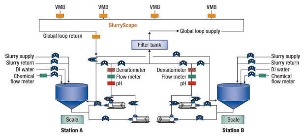
Figure 1. Configuration to correlate LPC to wafer CMP results. Establish LPC and wafer performance characteristics and correlations. Determine GL circulation effects on LPC values as a batch is consumed at the POU. SOURCE: Vantage Technology

At a recent CMP User conference, an industry spokesperson from a major chip maker said that the industry needs to move away from slurry dilution measurements, as they are not representative of the slurry condition during chemical mechanical planarization on-wafer results, and change the slurry condition [1]. Various issues with CMP slurry performance and related slurry quality drive demand for better metrology and testing. Tracking the difference between "as delivered" slurry at the fab-tank level, versus the "on-wafer quality" and results of the slurry on CMP wafers, is at the heart of the concern. Moving the slurry around the slurry delivery lines from sub-fab to CMP tools in the fab (Fig. 1) requires pumping, valves and shear stress that cause particle agglomeration — which in turn can cause scratching excursions.

According to studies on slurry handling in preparation for CMP processing, "Slurry turnovers through bulk slurry dispense systems and through fab piping will experience ~100 turnovers before being consumed." (R.K. Singh, from ref. #2) [2]. But the traditional use of slurry particle sensors that require dilution ratios as high as 20,000:1 to effectively measure the densely packed slurry particles has resulted in numerous diversions between the monitored slurry-sample test conditions and what is actually happening to the slurry used by CMP on the wafer. These dilution sensors are not measuring the slurry in the same conditions experienced by the wafer during CMP.

Slurry sampling and dilution for particle measurement effectively masks out the largest particle size bins, which are the most likely to cause scratching. The statistical probability for finding a few large particles when using only a few micro liters of slurry mixed with >1000× the volume of DI water (DIW) reduces large particle count (LPC) visibility to near-zero. Also, slurry dilution can affect its pH, its zeta potential, and can affect the iso electric point (IEP) — all factors in how much slurry tends to agglomerate or form larger, damaging particles. As presented in ref. #3, by Dr. Yuzhou Li, Ph.D, "Agglomerated particles may contribute to higher defectivity and yield loss in the CMP process. In general the chemical composition of slurries maintains a high repulsive electrostatic surface charge on abrasive particles to resist agglomeration. Aggressive handling may cause shear to the slurry abrasives due to strong velocity gradients produced by slurry flow by suddenly changing flow path and geometry [3]."

IC manufacturers need CMP slurry to perform consistently during the wafer polishing process, and to that end, they are pushing for improved slurry metrics. Only recently, new particle measurement units been developed that can monitor particles of undiluted slurry. In the past year, metrology system providers have developed new techniques that enable undiluted testing of slurries for both the LPC (i.e., >1.0µm) and the mean particle size of the slurry abrasives. Mean-sized particles — usually well below 100nm — are the slurry’s primary abrasives, with a tight distribution to control removal rates (RR). The LPC is associated with defects and scratching, because it is not considered to be part of the intended slurry composition, but can impact wafer polishing. Figures 2 & 3 show slurry particles in the LPC range measured down to a cutoff point with undiluted testing.
Click to Enlarge

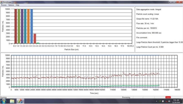
Figure 2. LPC cutoff ceria monitor >40hrs (SlurryScope data of undiluted measurements of slurry LPC). SOURCE: Vantage Technology

Figure 2 shows a graph of undiluted ceria slurry with the cutoff point where the slurry LPC reaches zero. The bars in the upper graph show particle size bins from 1.0µm and above, with the last two bins of 3.5-4.0µm (brown) and 4.0-4.5µm (green). The bottom graph is a time-line display (with the beginning of the test — time 0 at far right) of those two size bins over the >40 hour period of monitoring. The improvement or reduction in both size bins was the result of a new filter installation in slurry delivery line (note the drop in counts for both colors).
Click to Enlarge

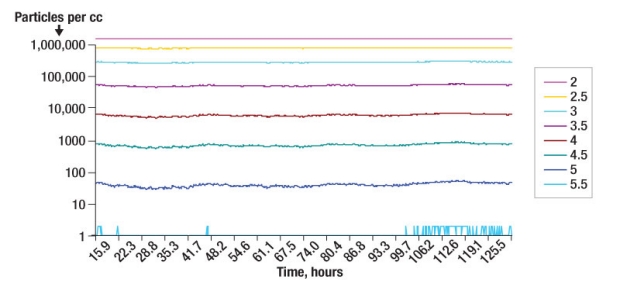
Figure 3. Ceria delivery monitor >120hrs. (SlurryScope data of undiluted extended run measurements of slurry LPC). SOURCE: Vantage Technology

Figure 3 shows longevity testing of ceria slurry over more than 120 hours with continuous monitoring of the size bins from 2.0 to 5.5µm, with the 5.5µm size just barely visible at the bottom of the graph. This is an example of undiluted slurry particle size distribution (PSD) measurement where the actual tail of curve can be tracked to zero — by comparison, the dilution sensor results are masked in size bins with smaller counts.

Other important parameters for controlling slurry quality, and thus predicting or improving CMP processing, include quantification of slurry reaction to induced shear-stress, and impact to the changes in zeta potential. Such test procedures are difficult to perform with controlled data comparisons. Modeling of a particular fab’s slurry delivery system to calculate the quantified shear-stress induced on slurry before it is deposited on the wafer is just one factor. Deciding on how to emulate and simulate the degree of shear-stress on new slurry during manufacturing is a significant obstacle for slurry developers or customers to test. However, it is this understanding of how slurry agglomerates with these handling forces that will enable the development of slurries with greater tolerance to shear-stress.
Click to Enlarge

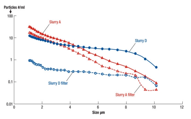
Figure 4. Effects of filters on particle measurement. SOURCE: Vantage Technology

Already, multiple IC manufacturers and CMP equipment companies are beginning to collect the data on a variety of slurries either at the slurry delivery and dispense point, or by starting to monitor the slurry in situ as delivered to the CMP system. Figure 4 shows the undiluted comparison of two different slurries before and after filtering. By monitoring post filter slurry PSD, it is possible to track the performance of the reduction in LPC and replace filters based on actual data. This represents another benefit to slurry quality at the CMP tool, rather than having to just change out filters on a recommended cycle basis.

Conclusion

Ultimately, the goal of measuring and tracking slurry particle distributions is to improve CMP results consistency, alert on or eliminate LPC growth that can cause defects, and minimize the cost impact to CMP systems by reducing lost utilization time to scratch excursions.

References:
1. "Characterization of abrasive particle distribution in CMP slurries," presented at Levitronix CMP Users Conference, Dallas, TX USA, May 11-12, 2011.

2. R.K. Singh, "CMP Slurry Metrology Characterization," 2007; Microelectronic Applications of Chemical Mechanical Planarization; p. 580; John Wiley & Sons, Inc.

3. Dr. Yuzhuo Li, Ph.D., Editor; Microelectronic Applications of Chemical Mechanical Planarization; "CMP Slurry Metrology Distribution and Filtration," p. 574; 2008 John Wiley & Sons, Inc.

Marty Mason received his BS from the US Naval Academy, and MBA from the U. of Santa Clara and is VP of Sales & Marketing at Vantage Technology Corp., 1731 Dell Avenue, Campbell, CA 95008 USA; ph.: 1-408-866-8522; [email protected]

Also read: The rule of three for CMP by Michael A. Fury, Techcet

Subscribe to Solid State Technology/Advanced Packaging.

Follow Solid State Technology on Twitter.com via editors Pete Singer, twitter.com/PetesTweetsPW and Debra Vogler, twitter.com/dvogler_PV_semi.

Or join our Facebook group