Category Archives: Metrology

Executive Overview

Two complementary techniques that provide in-line metrology solutions for epitaxial layers, such as SiGe or Si:C on Si wafers are presented. These techniques are high-resolution X-ray diffraction (HRXRD) and X-ray reflectometry (XRR). The capabilities and principles of both techniques will be summarized and representative data will be used to demonstrate both the principles and utility of combined HRXRD and XRR for the metrology of strained epitaxial layers. Both techniques are non-destructive and provide calibration-free, first principles measurement capabilities.

Paul Ryan, Matthew Wormington, Alexander Tokar, Jordan Valley Semiconductors, Durham, UK

Strain engineering is an accepted and important method to enhance the performance of advanced complementary metal oxide semiconductor (CMOS) devices. Process-induced local strain, is currently the mainstream technology used to increase the hole mobility in advanced pMOS transistors. Here, recesses are etched in the source and drain regions and SiGe is selectively deposited in the recesses to introduce uniaxial compressive strain in the channel. Electron mobility improvements in nMOS transistors have, to date, been largely achieved through the use of stress liners, but this technology becomes less effective with continued scaling. As such, selective epitaxial growth of Si:C in the source/drain is being developed as a method for introducing compressive strain into the channel for potential adoption at the 22nm node and beyond. As strain engineering is further adopted and refined by semiconductor manufacturers there is a need for improvements in the control of these processes.

In this article we will present two complimentary techniques that provide in-line metrology solutions for epitaxial layers, such as SiGe or Si:C on Si wafers. High-resolution X-ray diffraction (HRXRD) and X-ray reflectometry (XRR) can offer both accurate and precise measurements of thickness, composition, density and relaxation [1]. We will summarize the capabilities and principles of both techniques and describe a tool (JVX 7200) that has been developed for in-line measurements on product wafers. We will compare and contrast the new measurement approach with more traditional X-ray tools and discuss its advantages in terms of spot-size, throughput and reliability. We will present recent developments that allow XRR to be made on metrology pads within a scribe line. Representative data will be used to demonstrate both the principles and utility of combined HRXRD and XRR for the metrology of strained epitaxial layers.

High-resolution X-ray diffraction

HRXRD has been utilized for many years for the characterization and metrology of epitaxal thin films in both the compound and silicon semiconductor industries. Traditionally, the HRXRD technique has required a highly parallel X-ray beam (to ~10 arcseconds divergence) incident on the sample. The intensity of the diffracted X-rays is measured as a function of angle with respect to the sample surface, in a step-wise manner using a high-precision goniometer. By determining the incident and exit angles of the X-ray beam at intensity maxima in the spectrum, the strain, and hence lattice parameters, of the individual layers with respect to those of the substrate can be determined. These structural parameters can be converted to composition and relaxation of the layer in question using well known material relations. Thickness information of fully strained layers can also be determined from interference fringes that are present in the diffracted intensity from such samples.

A key disadvantage of the traditional HRXRD technique, especially on small metrology pads, is the low throughput. The comparable low intensity of an X-ray source compared to optical techniques, and the scanning nature of the technique lead to measurement times per point of several minutes. The in-line use of the technique in the silicon semiconductor industry has described [2] but has been typically limited to R&D and providing chamber qualification for the epitaxial reactors. One, or perhaps two, measurements were typically done using daily monitor wafers to check both the reactors and provide a baseline fast optical method, such as spectroscopic ellipsometery (SE), used for process monitoring of the product wafers. This approach was adopted largely due to necessity rather than being an optimal solution and such an approach is not without its problems. For example, correlations exist between composition and thickness measurement of SiGe layers using SE. The problems become much more acute at, and beyond, the 40nm node due to the use of multiple layer stacks and potential introduction of Si:C at 22nm, which typically only has a C concentration of ~1-2% compared with ~10-20% for Ge. This low composition essentially renders the Si:C layer invisible to optical techniques.

Figure 1. The Fast HRXRD method, using a convergent beam and 1D detector.

To help overcome these shortfalls with current epi layer metrology, we have developed a method for HRXRD that addresses the main issues hampering its use as an in-line metrology of high-quality epilayers on product wafers, i.e., low-throughput, and hence sampling, and spot size. The new method (Fig. 1) uses a focused, monochromatic X-ray beam incident on the wafer, with a one-dimensional detector. This enables all incident angles to be illuminated and the entire diffracted intensity to be acquired simultaneously. This approach allows HRXRD data from product wafers to be measured in tens of seconds rather than tens of minutes. This new FastHRXRD typically provides an order of magnitude speed improvement over conventional scanning measurements.

Figure 2. Comparison of FastHRXRD measurements of fully strained (green curve) and partially relaxed (blue curve) on a product wafer. Typical acquisition times for composition and thickness determination are ~100s.

Figure 2 shows two spectra collected on the new fast HRXRD system. Both spectra were collected in ~ 100 seconds from patterned wafers. The green curve shows data from a fully strained SiGe bilayer, with a clear SiGe peak on the left of the spectrum, from which composition is determined, and higher frequency fringes either side of this peak, from which the SiGe thickness can be determined. The blue curve shows a similar spectrum from a wafer where the Ge fraction was slightly too high and resulted in a partially relaxed test pad: the broad peak position gives information on the composition of the layer but, due to the relaxation present within the layer, no thickness fringes are seen. Therefore, the thickness cannot be determined from the HRXRD and an alternative method must be found.

X-Ray Reflectivity

X-ray reflectivity (XRR) is used for the measurement of thin, multilayer properties such as thickness, density, and roughness. XRR measurements are highly sensitive to the electron density of sub-micron structures irrespective of their crystalline nature. Consider an X-ray beam illuminating the surface of a sample at low (1-2°) incidence angle. The index of refraction for all materials in the hard X-ray wavelength region is slightly less than one, consequently, the X-ray beam is totally reflected if the incidence angle is a smaller than a certain critical angle. In this region, the penetration depth is only a few nanometers. At slightly higher angles, the X-rays start to penetrate and are reflected from the interfaces of thin-films resulting is a series of interference fringes. In the Jordan Valley system, a convergent beam illuminates all of these incident angles simultaneously, and a one-dimnsional detector enables parallel acquisition of the entire reflected intensity distribution in the detector of the XRR spectrum. This allows for extremely high throughput XRR, compared to more traditional scanning methods. Speed improvements of one to two orders of magnitude are typical with blanket wafer measurements taking only a few seconds per site.

Another limitation of XRR systems, to date, has been the length of the X-ray spot on the sample due to the glancing angle geometry. In the past, the smallest spot-size that was achievable was several millimeters. With the recent development of our latest generation of FastXRR (called VEGA), sub-mm spot sizes can be achieved and true scribe line measurements are possible. This has been done by improved control of the knife position allowing height above the wafer surface to be maintained at only a few microns.

Figure 3. Measured XRR data (blue curve) and best-fit simulation (red curve) from a 600µm test region (two adjacent 300μm SIMS pads) using the Vega FastXRR channel. Typical acquisition times for scribeline measurements is a few tens of seconds.

Figure 3 demonstrates the XRR data from two adjacent 300μm SIMS pads using the new channel. A clear interference pattern can be seen from the SiGe layer, allowing the thickness to be determined in tens of seconds. Furthermore, since XRR is not sensitive to the crystalline perfection of layers it can also be applied to amorphous and polycrystalline film stacks. This allows the FastXRR channel to also be used for metrology of other important front-end film stacks, such as those in high-k/metal gate processes or amorphous carbon hardmasks encountered for double-patterning and deep trench lithography applications where conventional optical metrology can struggle.

Combining HRXRD and XRR

The combination of the new HRXRD and XRR channels allows for the fast and accurate determination of all the critical SiGe parameters: thickness, composition and relaxation for process control. The combination can be extended to the determination of the individual layer parameters within SiGe multilayers for process diagnostics or during R&D.

Figure 4. High-speed maps of the Ge composition measured by Fast HRXRD (left) and thickness measured by Fast XRR (right) over a 300mm SiGe//Si(001) wafer.

Figure 4 shows how this combination works in practice for process control, with the composition and thickness of a SiGe layer mapped using the complementary techniques. By utilizing the strengths of each technique, the strain sensitivity of the diffraction and the thickness sensitivity of the reflectivity, unsurpassed accuracy and repeatability of the key SiGe metrics can be achieved to control the process.

Conclusion

The combination of HRXRD and XRR for the analysis and control of critical parameters of epitaxial growth has been presented with example data shown for SiGe layers. Significant improvements to each technique have been described including a new Fast HRXRD channel that improves throughput, as well as a reduction in spot-size for product monitoring of SiGe and Si:C. Additionally, a new channel can now perform XRR on scribe-line metrology pads, and not just blanket wafers, to enable product monitoring of a variety of front-end films. By using these complementary techniques, the JVX 7200 can determine the thickness, composition and relaxation of SiGe and Si:C layers with spot-size and throughputs suitable for in-line use.

References

1. D. K. Bowen, B.K. Tanner, X-ray Metrology in Semiconductor Manufacturing, Taylor & Francis (2006).

2. M. Belyansky, A. Domenicucci, N. Klymko, J. Li , A. Madan, Solid State Technology, 52 (2009)

Biographies

Paul Ryan received BSc(Hons.) and PhD degrees in physics from the U. of Leeds, UK, and is a Corporate VP/UK site manager for Jordan Valley. For more information, contact Alon Kapel at Jordan Valley Semiconductors IL Ltd, Migdal Ha’emek 23100, Israel; ph.: 972-4-6543666 x134, email [email protected].

Matthew Wormington graduated with a BSc(Hons.) in physics from the U. of Birmingham, UK and is the CTO at Jordan Valley Semiconductors.

Alexander Tokar received an engineering degree from Steel and Alloys Institute, Moscow, majoring in X-ray diffraction, and received his PhD from the Israel Institute of Technology (IIT) in materials science. He is a manager, worldwide application support at Jordan Valley Semiconductors.

More Solid State Technology Current Issue Articles
More Solid State Technology Archives Issue Articles

Executive Overview

As several leading chip makers assert a more specific time line for 450mm pilot line development, pre-competitive collaboration will continue to be the best path towards economic efficiency and industry rationality. While uncertainly about development funding remains, the supply chain is marshalling SEMI Standards task forces to advance agreements on the technical parameters for 450mm silicon wafers, physical interfaces, carriers, assembly and packaging. To date, SEMI has published six 450mm standards and 11 more are in the pipeline.

Jonathan Davis, SEMI, San Jose, CA USA

The relentless cost reduction and performance improvement of semiconductors is one of the most significant economic and social forces of the last half century. It transitioned the semiconductor industry into one of the world’s largest growth industries, helping improve and transform the lives of nearly everyone on the planet. A key driver behind this consistent ability to lower costs, improve performance and create new markets has been industry collaboration — the ability of the world’s smartest people to collectively work together to expand the industry. Pre-competitive collaboration systems like the International Technology Roadmap for Semiconductors (ITRS), SEMI International Standards, and other systems empowered Moore’s Law for a generation, focusing scarce R&D resources.

As the marketplace has consolidated and become truly global, industry organization and collaboration continues to be the foundation for progress and profitability. Not long ago, we faced the deepest industry slump in our 50-year industry; many fine companies did not survive the collapse in chip demand. Today, the economic outlook is brighter, but our industry remains vulnerable. As the global supply chain — IDMs, foundries, fabless chip companies and suppliers — approaches the multi-dimensional choices related to wafer size transition, pre-competitive collaboration continues to be the best path.

A credible or broadly-accepted 450mm wafer size transition scenario that validates overall economic benefit for the industry has yet to materialize. Many equipment companies and their suppliers remain skeptical about the business implications of a wafer size transition and uncertain about the funding for necessary development. However, several leading chip makers recently have been more assertive and specific about pilot line timing. A likely scenario — that involves participation of chip makers, policy makers, academic and research organizations, equipment and materials companies — is pressing forward, though many details remain closely guarded at the time of this writing.

Nonetheless, one thing is certain. If the transition is to ramp in the time frame desired by the primary proponents, much needs to be done to align industry activity, create efficiencies and agree on the fundamental specifications that enable development progress. To this end, the international standards community, working within the time-tested format of the SEMI International Standards program, has paved the way for necessary pre-competitive collaboration that is so essential for a successful transition.

ISMI has been active in supporting 450mm wafer development and material handling requirements through a number of programs and demonstration projects. They have created a "wafer bank" to lend test wafers to equipment developers, developed an interoperability test bed to support automation and material handling demonstrations, and created a set of equipment performance and EHS documents.

An update on 450mm activities in SEMI Standards

The SEMI Standards program is also making substantial progress towards enabling pilot development and providing a platform for future development work. SEMI has published six standards (Table 1) and is working on 11 draft documents relating to 450mm (Table 2). In addition, SEMI has organized standards task forces for 450mm silicon wafers, physical interfaces and carriers, and assembly and packaging.

The SEMI Standards program is overseeing increasing document development activities for 450mm-related standards, reflecting the increased attention and interest demonstrated by the SEMI Standards volunteers. Industry volunteers who are working on establishing standards on wafer specifications remind us of the original roots of the SEMI Standards program. With mechanical handling wafer, carrier, and load port specifications in place, the industry can cost-effectively continue the research and development of interfaces, processes, materials, and equipment which will be required for semiconductor manufacturing on 450mm wafers.

Specifications for 450mm front-opening unified pods (FOUPs) (SEMI E158-1110) and load ports (SEMI E154-1110) were developed to be used together, and are already available. Also, a specification for the interface between stockers and transport components is published as SEMI E156-0710.

While specifications for circuit-quality 450mm wafers are not yet in development, specifications are published for both mechanical handling wafers (SEMI M74-1108), which are used for R&D and semiconductor equipment design investigation; and single crystal wafers (SEMI M76-0710), which are used for process and metrology equipment R&D. Efforts are currently underway to develop a specification for 450mm polished wafer (Doc 5090).

The single crystal wafers specified in SEMI M76 can also be used to establish the techniques and metrology necessary to support a dimension specification for circuit-quality 450mm wafers. For the 450mm wafer size, edge profile and flatness need to be refined further than what has been used for smaller wafer sizes, and specifications for each of these are addressed by Doc 4588 and Doc 4812.

Figure 1. 450mm activity map.

A specification for a front-opening shipping box (FOSB) has been completed (Doc 4760), along with a specification for a new carrier for 450mm wafers, the Multi-Application Carrier or MAC (Doc 4770). The MAC is focused on silicon manufacturing and processed wafer shipping and is designed to be compatible with both load ports and especially FOUPs, using the same envelope, factory integration, and interoperability interfaces. Both 4760 and 4770 passed technical committee review. Draft Documents 4980 and 4981 modify SEMI E154 and SEMI E158 respectively to provide strong integration between FOUPs, carriers, MACs, and FOSBs. Also, with the completion of the shipping box activity, the next step is for the development of a specification for 450mm wafer shipping system (Doc 5069) that will address materials, dimensions and necessary items related to 450mm wafer shipping system, such as wafer shipping boxes, bags, labels, cushions, secondary containers, pallets, and shipping documentation.

On the assembly and packaging side, the Specification for Tape Frame for 450 mm Wafer, formerly Doc 4815, was recently published as SEMI G88-0211. Meanwhile, document development is in progress for specifications for frame cassettes (Doc 4814) and load ports for frame carriers (Doc 4965).

The expertise required for these documents is diverse, and for these future standards to work together, there must be cooperation across the technical committees sponsoring their development. An Auxiliary document is currently under development that would serve as a guide to how 450mm standards work together (Doc 5108).

The 11 "draft document" standards that are under development in accordance with an open and transparent consensus-based industry-wide process are listed in this chart.

SEMI 450mm Committee and Task Force structure

The current structure for SEMI 450mm activities involves three key technical committees that work together to make sure that the standards developed work effectively together.

  • Physical Interfaces & Carriers Committee: Develops specifications to enhance the manufacturing capability of the semiconductor industry, specifically mechanical, electrical, and special equipment specifications; and material movement integration, including substrate support and containment structures.
  • Silicon Wafer Committee: Develops standards for commercial silicon wafers, which includes specifications and guides for silicon wafers, test methods for silicon wafer quality and geometry, shipping box related topics, wafer ID related topics, and other issues that support communication between suppliers and customers.
  • Assembly & Packaging Committee: Develops specifications to enhance the manufacturing capability of the semiconductor industry as it relates to the packaging and assembly of the semiconductor chip, including the materials, piece parts, and interconnection schemes as well as the total infrastructure for chip to final set system and processes.

Conclusion

With dramatic cost reductions in the semiconductor industry, technology innovations have spurred enormous economic benefits throughout our lifetimes. With a growing consumer class in developing countries such as China and India, this economic progress can continue to fuel average annual growth rates of 8-10%. For over the last decade, sustaining Moore’s Law and industry cost reductions has been supported by highly-refined global collaborative processes such as the ITRS, SEMI standards, and industry consortia. As the global supply chain deals with wafer size transition, pre-competitive collaboration will continue to be the best path towards economic efficiency and industry rationality, and Standards play a major role.

Biography

Jonathan Davis is president, Global Semiconductor Business, SEMI, 3081 Zanker Road, San Jose, CA 95134 USA. For more information on SEMI, visit www.semi.org

More Solid State Technology Current Issue Articles
More Solid State Technology Archives Issue Articles
May 26, 2011 — Camtek Ltd. (NASDAQ and TASE: CAMT) received repeat automatic optical inspection (AOI) orders from an Asia-based foundry doing advanced micro bump inspection and metrology.

Systems should be installed during Q2 and Q3 2011.

3D IC technology is trending to advanced micro bumps (>10mm), and may reach up to 1 million bumps per die. Microbumps allow increased device interconnects on a small package footprint. Challenges arise in measuring such small bumps, including efficiently handling huge amounts of data, said Roy Porat, Camtek’s CEO, who expects that this customer will order more in the future. Camtek’s AOI systems combine high performance 2D and 3D metrology and inspection on one platform.

Camtek Ltd’s automated tools enable inspection of semiconductors and printed circuit boards (PCB) & IC substrates, using intelligent imaging, image processing, ion milling and digital material deposition. Learn more at www.camtek.co.il.

Subscribe to Solid State Technology/Advanced Packaging.

Follow Advanced Packaging on Twitter.com by clicking www.twitter.com/advpackaging. Or join our Facebook group

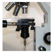
Click to EnlargeMay 24, 2011 — Sunrise Optical LLC debuted the Zebraoptical low coherence fiber optic interferometer with microscope attachment. The Zebraoptical Integrated Metrology Tool (ZIMT) provides metrology readings on micro electromechanical system (MEMS) wafers.
The tool’s standard Zebra wafer thickness and wafer topography metrology (ZebraOptical CT-IR) is paired with an optical microscope and VIS/NIR spectrometer. Users can measure substrate, membrane, and coating thicknesses and characterize coatings’ optical properties on the same tool platform.

A sample measurement service is available now. Learn more by contacting [email protected]. Lead time is currently 1 to 3 weeks ARO for the basic configuration.

Sunrise Optical LLC is an optical metrology company specializing in design and manufacturing of spectroscopic and imaging systems. www.zebraoptical.com.

Click to Enlarge
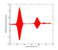
Zebraoptical Integrated Metrology Tool (ZIMT) interferometry measurement.

Follow Small Times on Twitter.com by clicking www.twitter.com/smalltimes. Or join our Facebook group

May 18, 2011 — Janice Golda, Intel, co-led a session at The ConFab 2011 on continued device scaling. EUV infrastructure will be a major topic, as well as transistor challenges. Device and materials options abound, but so does the risk.

Golda speaks with senior technical editor Debra Vogler.

The scaling roadmap will continue along Moore’s Law, scaling down to double density each generation. For 22nm and trigate, litho challenges are similar to what you’d have in other architectures, says Golda. There are more challenges in metrology and inspection, where defects easily hide in complex structures. Golda expects their session at The ConFab to demonstrate the interconnectivity of litho, wafer processing, and metrology challenges, as well as the business side of new technologies.

More from the ConFab:


May 5, 2011 – Marketwire — Tektronix Service Solutions, single-source provider of instrument calibration, repair and related services, was chosen by NXP (NQ:NXPI) to provide calibration and repair services for all test and measurement instruments at NXP’s production and development sites in the Netherlands.

The contract will be managed by the Fluke Service operation in Eindhoven on behalf of the Service Solutions Organization and will allow NXP to focus on its core business, leaving the calibration of its test and measurement instruments to the experts.

"Metrology plays a crucial role in the development and production of our products, and it is therefore vitally important to ensure that our test instruments are well-maintained and calibrated," said Leon Sintnicolaas, GM of the European Quality Labs at NXP Semiconductors. "When we decided to outsource the maintenance and calibration of our equipment…we chose Tektronix Service Solutions to take over this contract because we felt that they were able to offer the expertise and reliability we were looking for."

Tektronix Service Solutions provides asset management, calibration, repair, product and compliance testing, and quality certification. The company combines the service capabilities of Tektronix, Fluke and multi-vendor service teams of Davis Calibration and Sypris Test & Measurement into a single, service-focused organization. Learn more at http://service-solutions.tektronix.com/.

Subscribe to Solid State Technology/Advanced Packaging.

Follow Advanced Packaging on Twitter.com by clicking www.twitter.com/advpackaging. Or join our Facebook group

Gabriel Monette, Université de Montréal, Montreal, Canada and Marc Verhaegen, Photon etc., Montreal, Canada

Magneto-optical (MO) effects are used as tools for probing the magnetization reversal characteristics of a wide range of sample types, and as an effective way to modify the polarization of light via induced magnetization state in samples. In transparent samples, the Faraday effect (rotation of the polarization of light proportional to the magnetic induction field and optical path in the medium) can be used to elaborate Faraday rotators, a key element in the design of optical isolators [1]. Along with other MO effects such as Kerr measurements, they provide a non-destructive probe for in-situ measurements of samples, such as thin films.

Spectral dependence of the Faraday MO effect in the visible part of the electromagnetic spectrum along with temperature dependence measurements were performed on a semiconductor 2micron epilayer (GaP) grown with embedded metallic ferromagnetic nanoclusters (MnP). The confined geometry of the experiment — which necessitates a cryostat chamber with optical window placed within the pole gap of an electromagnet applying the DC magnetic field parallel to the normal of the sample — made it difficult to use a monochromatic light beam produced by filtering an incandescent light source with a standard monochromator.

Click to Enlarge

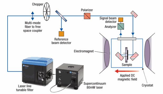
Figure 1. Experimental set up.

Instead, the team used a collimated tunable laser based on a Leukos (SP20) supercontinuum source and Photon etc’s Tunable Laser Line Filter. Figure 1 shows the experimental set up used to investigate the MO properties of the GaP:MnP in the Faraday configuration. The analyzer is mounted on a motorized rotation stage to allow tracking of the extinction condition as a function of temperature, wavelength and applied magnetic field. Hysteresis curves were obtained by rotating the analyzer at 45° with respect to the polarizer and sweeping the magnetic field from -400 to 400 mT. Small angles of rotation ensure linear variation in transmitted intensity as a function of the rotation angle of the polarization, or applied magnetic field. The source of the electromagnet, the temperature controller for the cryostat, the angular position of the analyzer, and the wavelength selection of the laser output (via Photon etc Tunable Laser Line Filter) are all computer controlled. The angle of rotation must be obtained independently for each applied field, wavelength, and temperature.

Click to Enlarge
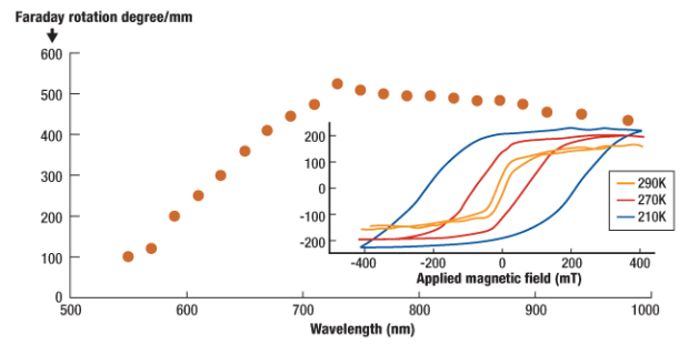
Figure 2. Faraday rotation vs wavelength.

The total Faraday rotation of the epilayer as a function of wavelength at a temperature of 220K is displayed in figure 2. The free carriers contribution of the GaP substrate has been carefully substracted. The GaP:MnP epilayer produces a maximum MO effect in the near infrared, whereas the substrate has a monotonic decrease in the MO effect as the wavelength is increased. The inset shows the Faraday rotation hysteresis curves at 210K, 270K and 290K at 655nm. The giant Faraday rotation in these systems has been reported [2]. The tunable laser allowed us to investigate the hysteresis signature of the MO Faraday effect at different wavelengths as well as different temperatures within the limited work space of the apparatus.

Future applications

Although this specific experiment and material (GaP:MnP) aim at a better understanding of the underlying physics of effective medium, i.e. the interaction between EM-waves and metamaterials made of metallic nanoclusters embedded in a semiconductor host matrix, it can be applied to develop new, easily integrated opto-isolators. Magneto-optical effects in general can be used for a wide range of applications, from data storage and processing to thin films characterizations or even remote magnetic field sensors. The Faraday effect in particular is of paramount importance in modern optical networks for it is the very corner stone for devices such as isolators and circulators.

REFERENCES
[1] T. R. Zaman, X. Guo and R. J. Ram, Semiconductor Waveguide Isolators, Journal of Lightwave Technology, 26, 2, (2008)
[2] G. Monette, C. Lacroix, S. Lambert-Milot, V. Boucher, D. Ménard and S. Francoeur, Giant magneto-optical Faraday effect in GaP epilayers containing MnP magnetic nanoclusters, Journal of Applied Physics, 107, 9, (2010)

Marc Verhaegen, PhD, 5795 Gaspé av., #222, Montreal, H2S2X3, QC, Canada; ph.: 514-385-9555; [email protected]

By Debra Vogler, senior technical editor

April 13, 2011 — New work from Stanford University goes beyond simple bump shear testing to allow simulation of stresses exerted on chips during semiconductor packaging. The researchers are able to explore how the stresses affect back-end structures.

Alex Hsing, a PhD student in Professor Reinhold Dauskardt’s Group at Stanford University, will be presenting a paper titled "Shear microprobing of chip-package interaction in advanced interconnect structures" at the IITC 2011 Conference (May 9-12, Dresden, Germany). In a podcast interview, Hsing summarizes the key results of the paper and explains how the group’s approach differs from simple bump shear testing.

Click to EnlargeListen to Hsing’s interview:  Download or Play Now

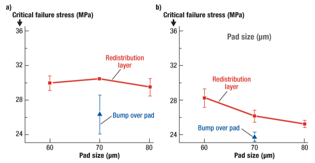
The researchers used a microprobe metrology system to evaluate advanced interconnect structures, studying a bump-over-pad design vs. an RDL design at three temperatures (room temperature, 50ºC, and 100ºC). At room temperature and 50ºC, the bump over pad design and the RDL design behave in a "relatively comparable manner." However, at 100ºC, the bump over pad design weakens significantly compared to the RDL design (see the figure). They concluded that the "comparatively lower temperature sensitivity of critical failure stress of the RDL design suggests that it may offer an advantage at high temperature," as noted in the paper. The group showed that shear stresses cause damage that can quickly propagate through multiple levels of metal.

Click to Enlarge

Figure. Critical failure stresses for the bump over pad design and the RDL design plotted as a function of pad size at 100ºC in the stronger direction (a), and in the weaker direction (b).

Hsing also addresses the anticipated "hot button" issues that will likely come up at the conference, and the next steps the researchers will take, (e.g., imaging methods will be needed to pair up with the metrology system described in the current paper).

Subscribe to Solid State Technology/Advanced Packaging.

Follow Solid State Technology on Twitter.com via editors Pete Singer, twitter.com/PetesTweetsPW and Debra Vogler, twitter.com/dvogler_PV_semi.

Or join our Facebook group

March 15, 2011 — KLA-Tencor Corporation (Nasdaq: KLAC), process control and yield management provider for semiconductor and related industries, introduced the ICOS CI-T620, a high-performance component inspector system for tape and reel.

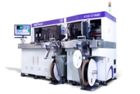
Click to EnlargeAn addition to KLAC’s Component Inspector series, the CI-T620 is a fully automated optical inspector of integrated circuit (IC) packages for 3D measurements and package quality with dual tapers for improved output. Tape and reel is a process of packing surface mount devices by loading them into individual pockets within a pocket tape or carrier tape. The units are sealed in the carrier tape with a cover tape. The carrier tape is wound around a reel for handling and transport. The CI-T620 system has dual tapers working sequentially with minimal operator intervention to increase units per hour.

3D metrology inspection down to 5mm and high-resolution imaging capture surface defects down to 40µm. The system boasts faster package changeover (<5 minutes) and a throughput increase of up to 80%, compared to current industry methods. A complete portfolio of unique 2D and 3D inspection capabilities is supported by KLA-Tencor’s proprietary technology, and compatibility with a broad range of packages and sizes: 3 x 3mm to 42.5 x 42.5mm

KLA-Tencor’s component inspector system will be introduced at SEMICON China, taking place March 15-17 at the Shanghai Convention and Exhibition Center.

KLA-Tencor Corporation (NASDAQ: KLAC) provides process control and yield management products for the semiconductor, data storage, LED, photovoltaic, and other related nanoelectronics industries. Additional information may be found at www.kla-tencor.com.

Subscribe to Solid State Technology/Advanced Packaging.

Follow Advanced Packaging on Twitter.com by clicking www.twitter.com/advpackaging. Or join our Facebook group

March 14, 2011 – PR.com — CAPRES A/S, a Danish developer of next-generation semiconductor metrology systems for the direct nano- and micro-scale electrical characterization of materials, announced a repeat order for its fully automated 300mm microRSP-A300 from an industry-leading semiconductor foundry in Asia.

Delivery and installation of the new metrology order will occur in May 2011 and follows the successful evaluation of the first one delivered in 2010.

With the development and production release of the microRSP-A300, CAPRES has addressed the challenges associated with in-line measurement on production wafers, reducing reliance on data extrapolation and monitor wafers to validate doping levels.

This production application of micro-scale sheet resistivity measurement allows, for the first time, immediate detection of process deviations thereby shortening the production control loop and enabling a commensurate reduction in work-in-process and losses due to out-of-specification production processes.

This customer finds that conventional Rs and optical metrology tools are not capable of measuring the sheet resistance of the very thin conductive films needed for production processes beyond the 40nm node, said Bo Hansen, CEO of CAPRES A/S, who suggests that many companies agree that optical metrology and Rs are not sufficient.

CAPRES A/S supplies micro-scale metrology systems for the semiconductor and magnetic storage industries. CAPRES metrology products use patented MEMS-based probe technology and are available in manual and fully automated configurations. More information is available at www.capres.com

Subscribe to Solid State Technology/Advanced Packaging.

Follow Solid State Technology on Twitter.com via editors Pete Singer, twitter.com/PetesTweetsPW and Debra Vogler, twitter.com/dvogler_PV_semi.

Or join our Facebook group