Category Archives: Metrology

(July 22, 2010) — These market statistics were compiled by Nancy Wu & Mary Olsson, part of the Gary Smith EDA team. The biggest change in 2009 was Mentor passing Cadence to become number two in product sales in EDA. This is an indication of the market shift caused by the move into the ESL Methodology. Synopsys remains a strong number one.

Mentor also grabbed #2 overall in IC design. With the acquisition of Valor, Mentor is also now 3× as large as its next competitor in PCB design.

We believe that the recent changes in Cadence has stopped their market share decline, similar to the changes made at Mentor, bringing in Walden Rhines, during the switch to the RTL design methodology.

Table. Market Share 2009. Note: All numbers show the best estimates of the Gary Smith EDA Analyst. Source: Gary Smith EDA (June 2010)
Rank  2008  2009  Growth, 2008-2009  Market share, 2009
Synopsys 1,227.40   1,250.45   1.9% 31.0%
Mentor Graphics 755.10 758.50   0.5% 18.8%
3   Cadence Design Systems    905.12      746.08   -17.6%  18.5%
Magma Design Automation       159.50      113.80   -28.7% 2.8%
Agilent EEsof       110.10      113.40   3.0% 2.8%
Other  1,074.15 1,051.56   -2.1% 26.1%
All companies 4,231.37   4,033.78   -4.5% 100.0%

Gary Smith EDA Market Statistics are a continuation of the Dataquest EDA Market Statistics that were started in 1985. Gary Smith EDA Market Statistics consist of Market Share, Market Forecast and Market Trends. In order to better serve the start-up community, Gary Smith EDA splits Market Trends into five reports. Basic Service consists or a minimum of one Markey Trend report and ten hours of Inquiry. For more information, visit http://www.garysmitheda.com/contact.php

In this video interview from SEMICON West 2010, Walden Rhines, Mentor Graphics, discusses 3D technologies. EDA tools need to be extended to meet the needs of 3D — parasitic extraction and timing, place-and-route, and other steps are different with 3D. The tools are evolving for various 3D techs.

To watch a video interview with Segare Kekare, Synopsis, about rapid root cause analysis and process change validation using design-centric volume diagnostics, go to: Yield metrology looking at systematic failure mechanisms: Synopsis

(July 15, 2010) — Alok Vaid of GlobalFoundries, explains the technology in his paper on time-to-solution for scatterometry metrology. Scatterometry takes a long time, but Vaid proposes a new approach with more automation.

More from Global Foundries at the show:
Global Foundries lays out road-map for advanced silicon
AMD spin-off Global Foundries has been detailing how it will overcome the technical challenges of mass producing silicon hardware at 28nm and beyond.
Read the story from SEMICON West at http://www.electroiq.com/index/display/semi-wire-news-display/1222823641.html

Get all the latest news, podcasts, videos and more from SEMICON West at http://www.electroiq.com/index/Semiconductors/semiconwest2010.html

by Mike Fury, Techcet

Click to EnlargeJuly 14, 2010 – The first day of SEMICON West 2010 kicked off with a keynote address by IBM’s Bernie Meyerson, who has become a perennial favorite at the podium. His talk, "From Ghz to systems to solutions; our industry in transition," provided some insights on how Moore’s Law is morphing from device scaling to system scaling. Along the way, additional attention is being focused on enabling global IT networks while still leaving enough spare electrical power for us to operate our hybrid cars and HDTV home entertainment systems. It’s a shame that keynote addresses so often command the broadest audience but are most frequently the very talks for which slides are not available to attendees.

Rob Rhoades, CTO at Entrepix, reports that they’ve been seeing a lot of requests for refurbished CMP tools from non-CMOS clientele, for applications including MEMS, TSV, LED and other compound semiconductors. The consumable materials for these non-standard processes are still being adapted from available semiconductor product lines, as these market opportunities are still generally regarded as too small to justify customized product development.

Marty Mason at Vantage Technology gave me a quick tour of their real-time, undiluted CMP slurry particle monitoring system. Slurry flows through the system at 30 ml/minute and produces a real-time histogram of particle size distribution from 0.9-9.9μm, with the ability to go as high as 20μm. There is some additional capability at the low-end as well, though this seems to be of more interest to slurry developers than to line engineers.

Speaking of CMP, the NCCAVS has scheduled sessions during SEMICON West for the CMP User Group (Wednesday 1-5pm), and on Thursday for the Junction Technology Group and the Plasma Applications Group (both 11am-3pm). AVS is also sponsoring the International Conference on Planarization/CMP Technology (ICPT) in Phoenix, November 14-17.

Pat Levy at Pall Microelectronics gave me a quick tour of their latest filter product introductions. For CMP slurry applications, the Profile Nano Filter is a multi-layer web of melt-blown nanofibers about 50% smaller than their previous generation. In addition, while earlier products were spec’d at the cartridge level, this product line is spec’d at the level of individual filter media layers. The net result in performance on both silica and ceria slurries was a 30% decrease in microscratch defects on the polished wafer surface, compared to their prior generation filter. For broader fab applications, a new generation of filters for surface preparation applications is the Ultipleat line, made with polyarylsulfone rather than a Teflon-related backbone. This allows particle capture to 10nm vs. a 20nm minimum for Teflon. The filter media also incorporates a pore size asymmetry from one side to the other, providing for maximum particle capture with minimum pressure drop, and therefore high fluid flow rates. This product line is intended for functional surface prep chemistries line DHF, BOE, and even more aggressive agents.

Woo Sik Yoo, CTO at WaferMasters, had an unmet metrology need for characterizing the results of wafer thermal processing in their hot wall, isothermal processing chamber. Sometimes you just have to invent something yourself to meet that need, but coming up with a suite of three unique measurement tools is a sure sign of an over-achiever. WaferMasters is introducing their metrology products this week. These include multi-wavelength Raman and photoluminescence, and an optical surface profilometer. These can produce both chip-scale and wafer-scale results.

Ceimig Ltd. of Dundee, Scotland, has shown up with the Scottish Enterprise group of small companies and startups. Several suppliers already provide ALD precursors for BKM tool recipes. Ceimig is a step further back in the R&D pipeline, offering custom synthesis of organometallic compounds for evaluation as ALD precursors, with a focus on platinum group metal compounds. For emerging semiconductor applications, this includes such favorites as Hf, Ru, and Ir.

The folks at Megasonic Sweeping. are very pleased with the level of interest they are receiving for their batch cleaning megasonic transducer tanks. The bulk of their business is in retrofit kits for 200mm wafer tanks. This caught my attention because it is yet another indicator that, in this industry, we are very quick to predict the demise of old technologies but rather slow to bury any bodies. I worked on megasonic cleaning at IBM in the 1980s, and since then obituaries have been posted many times over both for batch cleaning and for wet cleaning. Both seem to be alive and well — like their other zombie cousin, optical lithography.

In wandering the show floor, the astute observer may notice that the floor today is smaller than the floor of years gone by. Many of the nooks and crannies once filled by smaller booths are empty. Several meeting venues have been moved onto the main show floor, instead of being held in closed conference rooms. It remains to be seen if this open environment is suitable for all of the meetings, if for no other reason than the background noise and distractions from casual passers-by. I will be able to judge this for myself, at the aforementioned NCCAVS CMPUG session Wednesday afternoon on the Moscone South TechSITE stage.

On a personal note, I am very gratified by the number of folks who have asked me if I would be blogging on this SEMICON show, as they’d seen my MRS, ECS, and IITC blogs and had come to expect more. As I understand it, this is how crack dealers establish their clientele, starting with free samples and then increasing their expectations. Unfortunately, I have no good ideas how to monetize this as effectively as a crack dealer does, and am open to suggestions.


Michael A. Fury, Ph.D, is senior technology analyst at Techcet Group, LLC, P.O. Box 29, Del Mar, CA 92014; e-mail [email protected].

(July 8, 2010) — Lasertec Corporation of Japan has joined SEMATECH’s 3D Interconnect program at the College of Nanoscale Science and Engineering (CNSE) of the University at Albany. Lasertec will partner with SEMATECH to develop robust, cost-effective process metrology technology solutions for readying high-volume via-mid through silicon via (TSV) manufacturing. 

The collaboration between Lasertec and researchers from SEMATECH’s 3D Interconnect program will include investigations and comparisons of 3D TSV depth metrology schemes. This work is necessary not only for TSV RIE process control, but also for providing critical feed forward data for wafer thinning and TSV expose processes. To facilitate this work, Lasertec will place a 300 mm TSV infrared (IR) etch metrology tool in SEMATECH’s 3D R&D center, providing advanced measurement capabilities that will enable accurate, repeatable TSV depth measurements over a range of TSV dimensions.

“We are pleased to welcome Lasertec to the 3D program,” said Sitaram Arkalgud, director of SEMATECH’s 3D Interconnect program. “Our common goal is to address the technical challenges of via-mid TSV technology. The metrology expertise of Lasertec combined with the capability of the TSV 300-IR will fill an important gap in our integration scheme. Together, we will provide our members with a world class TSV depth metrology solution capable of addressing today’s needs as well as tomorrow’s aggressive dimensions.”

Sitaram Arkalgud, Sematech, summarized the company’s 3D metrology to measure TSV depths and profiles. This technology is important to determine how far to thin wafers. He also updates SST/AP on TSV standardization.

Get all the latest videos, podcasts and news from SEMICON West 2010 at http://www.electroiq.com/index/Semiconductors/semiconwest2010.html

“Lasertec is looking forward to contributing our expertise in the fields of metrology and inspection to further explore innovative metrology capabilities that will make 3DTSVs commercially viable,” said Hal Kusunose, CTO of Lasertec. “Our cutting-edge TSV 300-IR tool will allow SEMATECH researchers and SEMATECH’s member companies to address important metrology challenges of TSV technology.”

“The leading-edge R&D that is critical for commercializing innovative TSV technologies will be further enhanced by the addition of Lasertec to CNSE’s Albany NanoTech Complex,” said Richard Brilla, CNSE VP for strategy, alliances and consortia. “This new collaboration builds on the SEMATECH-CNSE partnership to support the advanced technology needs of our global corporate partners and the nanoelectronics industry.”

TSV technology is a method of combining integrated circuits (ICs) in a vertical stack to enable high functionality and performance with low power consumption in a small footprint. While employing many standard chip manufacturing and packaging processes, TSVs present several new technical and logistical challenges, now being addressed by SEMATECH.

SEMATECH’s 3D program was established at CNSE’s Albany NanoTech Complex to deliver robust 300 mm equipment and process technology solutions for high-volume TSV manufacturing. To accelerate progress, the program’s engineers have been actively engaging with leading-edge equipment and materials suppliers. Eventually, 3D interconnects will provide cost-effective ways to integrate diverse CMOS technologies and chips with emerging technologies such as micro and nano electromechanical systems (MEMS, NEMS) and bio-chips.

Lasertec supplies innovative semiconductor, LCD and PV related inspection and measurement equipment: TSV etching depth inspection system, wafer inspection/review system, EUVL mask blank inspection system, photomask inspection system, photomask haze removal system, color filter repair system, PV cell conversion efficiency distribution measurement system and various types of confocal laser microscopes. For more information, go to www.lasertec.co.jp.

The UAlbany CNSE college is dedicated to education, research, development, and deployment in the emerging disciplines of nanoscience, nanoengineering, nanobioscience, and nanoeconomics. The UAlbany NanoCollege houses the only fully-integrated, 300mm wafer, computer chip pilot prototyping and demonstration line within 80,000 square feet of Class 1 capable cleanrooms. For more information, visit www.cnse.albany.edu.

Executive Overview

As the semiconductor market begins to recover and customers begin to order new products in higher volumes, product competitiveness, and time-to-market will be absolutely critical. This is a good time to take stock of your development readiness and to understanding how well legacy software assets will support the product roadmap.

Dan O’Connor, Foliage, Burlington, MA USA

The software development community is known for inventing useful metaphors as a means to relate technical topics to "real world" concepts. The technical debt metaphor was first introduced by Ward Cunningham [1] to compare deficiencies in software with financial debt, a topic that is now all too familiar for most of us. Just as the U.S. will pay the penalty for excessive financial debt with slower growth and less economic competitiveness for the next few years, excessive technical debt has the impact of slower development velocity and reduced product competitiveness.

There are many situations where a development team will decide to ship a product with known deficiencies in the software design and/or implementation. The code freeze date was announced months ago and there is a scramble to get the feature enhancements completed. Consequently, additional shortcuts are taken. Finally, the decision is made to move forward. Ship it! Any additional improvements will have to wait until later. But later too often translates to never; it is all too easy to forget about those shortcuts and deficiencies after the product is released and the organization moves on to product support and enhancement activities. This is an example of technical debt; it must be recognized to be serviced one way or another.

The technical debt metaphor turns out to be a useful vehicle for communication between product development teams and executive management, who otherwise may not be eager to invest resources in cleanup tasks, redesign, or refactoring. Servicing debt, however, is a concept that management does understand, and its importance tends to sink in when development can identify the specific costs associated with long term, unattended debt.

Deliberate debt and the downturn

Martin Fowler adds an interesting perspective with his classification of technical debt into quadrants [2]. His suggestion is to distinguish between deliberate and inadvertent technical debt as well between prudent and reckless debt.

It’s likely that most equipment control systems have accumulated deliberate technical debt during the last several years. Many capital equipment firms have been running on a skeletal R&D staff for several years as software development organizations have been impacted more than in previous down cycles. General managers have been faced with difficult cost-cutting decisions and in many cases have had to put R&D on ice to wait out the downturn.

In this environment, it is prudent to take on some technical debt. In many cases there are very few feature enhancements being made; only critical bug fixes will be released. There are simply not enough development resources and budget available to make significant improvements in the software.

Assessing technical debt

It is clear that, with the anticipated market upturn, equipment suppliers will again be challenged to support the next semiconductor design node and the fabs will begin to make demands for new features and new tools. Process and metrology tools will require finer accuracy to meet ever-decreasing critical dimensions.

Technical debt can manifest itself in many different ways. There are several familiar clues to look for however, and tools can also help identify potential problem areas.

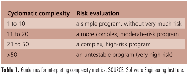
Complexity. Complex code is a fundamental sign of technical debt. Many legacy control systems have a few infamous code modules that are difficult to maintain. You may have heard statements such as, "No one understands how the recipe manager works" or, "The scheduler code is too fragile, only Steve can modify the scheduler." If these comments resonate, then you have experience with technical debt and the consequences of reduced ability to modify or enhance modules or poor reliability due to the inability to appropriately test the application. McCabe cyclomatic complexity is the most common complexity metric and many static analysis tools can easily calculate the measurements for your project. The Software Engineering Institute [3] publishes guidelines for interpreting complexity metrics (Table 1).
Click to Enlarge

Code duplication. When a code freeze is approaching, "cut and paste" can be a favorite approach in the developer’s bag of tricks. This is classic technical debt: shortcut, now, pay for your sins later.

Documentation debt. The next item that tends to get jettisoned at the release deadline, or during periods of tight development resources, is documentation. Developers are not known for being enamored with documentation in the first place. Lack of documentation does not directly affect the runtime characteristics of the software system, but missing design or test documentation needs to be counted as technical debt because there is interest to be paid.

Testing debt. Unit testing is another item that gets squeezed due to schedule pressure. The interest on this type of debt is the lack of a safety net to catch regressions. Current best practices in software development call for unit tests for all modules and for running all tests during continuous integration. Michael Feather calls this "code that bites back," [4] meaning that the system informs you (usually by email) if your submission just broke a unit test. Again, good code coverage tools exist to help you understand your testing debt.

Architectural debt. Architectural debt exists when the software architecture is no longer well-aligned with the key product drivers and this can happen in two ways. First, developers can cause architectural decay if they do not understand and follow the architectural rules and maintain the intended conceptual integrity. A good example is not following the architectural layering rules and perhaps introducing a circular dependency. The second path to architectural debt is when the product itself evolves well past the capability covered by the original architectural design. This often occurs with very successful products or product lines; if the market loves the initial product capability, it tends to want to leverage it in new applications and demands additional features, modifications and configurations.

Tracking technical debt

It is important to make these different types of debt visible. Some agile development teams use informal debt statements, written on index cards and posted on a bulletin board. Other organizations use a more formal tracking method which calls for developers to enter debt issues into the tracking system. This allows the organization to prioritize the issue and estimate the time for the required refactoring. It also allows the debt issues to be added to the schedule and to be managed like any other development task.

Another established, but simple, effective method is the use of a "pain dashboard" to track technical debt. This can be manifested as a wiki page where developers could easily add entries describing the parts of the system that are difficult to understand and debilitating to their productivity. The system can allow for a voting scheme so the team has a self-balancing mechanism to continually prioritize their technical debt.

Bankruptcy as the last resort

When faced with crippling financial debt, bankruptcy is always the last resort. We can extend the technical debt metaphor nicely here. For equipment control systems, bankruptcy occurs when you conclude that the legacy code base is a dead end and is no longer viable to support the forward-looking product roadmap. A complete rewrite and a new platform are needed for the organization to be competitive going forward. In this case, the technical debt can be retired along with the legacy system, and like filing Chapter 11, you are no longer responsible to address all the sins of the past.

Initially, this may sound like an attractive option, but the decision to undertake a rewrite should never be taken lightly. Developers rarely get the opportunity for a clean sheet redesign, and for good reason; it is expensive. Developing a new equipment software platform can represent an investment of perhaps millions of dollars.

Still, it is true that control system software does have a finite shelf life. If the existing equipment software is ten or more years old, there is a good chance that it does not leverage advanced off-the-shelf software technologies or modern design and architecture concepts. A redesign represents an opportunity to significantly increase the productivity of your software staff (with a resultant cost reduction) as well as a chance to retire a decade of technical debt en masse.

Benefits of paying down the debt

Your software control systems have, more likely than not, incurred significant technical debt during the economic downturn. It’s time to pay down the technical debt and your organization will benefit:

Increased R&D efficiency and improved time-to-market. Once the code base has been cleared of crippling technical debt, the development velocity will increase. The design refactoring is effectively cleaning the molasses out of your software development machinery. You can expect subsequent software modifications to be implemented more efficiently, and therefore, time-to-market for new features and new products will improve.

Hitting commitment dates. Paying down the technical debt will increase the team’s overall understanding of the code base. This will have the effect of getting better estimates for work to be completed and reducing risk during subsequent modifications.

Performance and technology upgrades. Another positive side effect of attacking the technical debt is the opportunity to upgrade to the latest technologies. This can mean moving to the latest versions of compilers and development tools. It can also mean upgrading to the latest versions of the operating system and third-party libraries and possibly even to a faster processor.

References

1.  http://c2.com/cgi/wiki?TechnicalDebt

2. M. Fowler,  http://martinfowler.com/bliki/TechnicalDebtQuadrant.html

3. Carnegie Mellon, Software Engineering Institute.  http://www.sei.cmu.edu/

4. M. Feathers, Working Effectively with Legacy Code. Prentice Hall, Englewood Cliffs, NJ, 2005.

Biography

Dan O’Connor received his MS in computer science from Boston U. and is a software architect at Foliage, 168 Middlesex Turnpike Burlington, MA 01803; ph.: 781-993-5500; email  [email protected].

More Solid State Technology Current Issue Articles
More Solid State Technology Archives Issue Articles

by Griff Resor, Resor Associates

February 22, 2010 – The SPIE Advanced Lithography Conference in San Jose, CA, provides a once-a-year opportunity to see the future of IC manufacturing. For years, this has been the conference where experts in lithography, resists, metrology, and design come to tell about their recent advances. Typically the good ideas move into IC production within two to three years.

Everyone will be watching the battle between optical lithography and EUV, which for the first time will have its own conference. The EUV conference has 127 papers — compared to 124 for the optical lithography conference, a huge advance for EUV in just one year — mostly aimed at high-volume insertion at the 22nm node by 2013. It will be interesting to learn how attendees feel about this schedule. Key challenges for EUV remain mask defects, resist resolution, and line-edge roughness (LER), and source power. As source power increases, there is a renewed concern for the lifetime of mirrors in the EUV optical train. I expect to hear credible evidence that progress on resist, sources, and lifetime will support the schedule. Progress on EUV mask defects is not so certain, so will set the pace from this week on.

The optical lithography conference has 124 papers, evenly split between the 32nm and 22 nm nodes. Computer modeling to optimize what’s left for a process window is the #1 topic (30 papers); double patterning comes in second (17 papers). For several years now it has been clear that some form of double patterning lithography (DPL) would be required to move optical lithography to the next node. Many variations on this theme will be reported this week. With overlay error budgets in the single digits of nanometers, masks and matching of scanner tools are also key topics.

A quick scan of the resist track’s 123 papers provides a sanity check on the EUV vs. optical lithography battle. Thirty-six of the resist papers describe optical and DPL materials and methods; 18 papers discuss products for EUV use. Many papers describe generic improvements in materials. It seems that material suppliers still see a larger market for optical and DPL products than for EUV products.

Three emerging technologies are the focus of the "alternative lithography" track. 26 papers describe direct writing tools, most using multi-beam e-beam. IC foundries such as TSMC are pushing for these tools as a workaround to the ever higher cost of masks for optical and EUV lithography. Nano-imprint lithography (NIL) continues to conquer new applications — structured media for high-density disk drives looks like a natural, and will be covered this week. Finally, self-assembly techniques continue to get attention, as nano-structures built in the IC industry and biotechnology converge.

After a busy week, Griff will report on his findings at this key lithography conference next week.


Griff Resor, an SST editorial advisory board member, is president of Resor Associates, ph 978-897-2200, e-mail [email protected].

(January 28, 2010) EINDHOVEN, The Netherlands — The EuroPIC project aims to facilitate access by small companies to cost-effective photonic integrated circuit (PIC) manufacture in Europe. It also will encourage research on manufacturing methods to develop an open-access industrial generic foundry production capability for Europe. EuroPIC is a collaborative project formed by a consortium of experts, consisting of a mix of small- to medium-sized enterprises (SMEs), industry, and academic partners in the fields of component manufacturing, PIC design and applications, photonic CAD, and packaging.

EuroPIC received €3.75 million funding from the European Community’s Seventh Framework Programme (Directorate General for Research, Directorate Industrial Technologies—G2: New Generation Products) to effect a fundamental change in the way applications based on photonic ICs are designed and manufactured in Europe. The key development is to facilitate access by small companies (SMEs) to development and manufacturing of photonic micro-systems in the form of advanced but very cost effective PICs. EuroPIC will bring forth a new production paradigm to forge a sustainable business sector with the potential for very significant future growth. This will be done by developing a generic technology that is capable of realizing complex PICs from a small set of basic building blocks. The program adopts a holistic approach addressing the whole production chain from idea, via proof of concept, design and prototype to product and application.

The consortium will carry out research into manufacturing methods and high-throughput processes that can lead to an open-access industrial generic foundry production capability for Europe. It will demonstrate the potential of the generic approach by fabricating a number of application-specific PICs (ASPICs) with a record combination of complexity and performance, for a wide range of applications in telecommunications, sensors, data communications, medical systems, metrology and consumer photonics.

Further, EuroPIC is building a strong User Group, many of them SMEs, with committed users from different application fields, which will be actively involved in introducing cost-effective ASPICs in a variety of novel applications, providing Europe with a competitive advantage over the US and the Far East. Partners in the EuroPIC consortium include project coordinator COBRA (Technische Universiteit Eindhoven — TU/e), Willow Photonics Ltd (U.K.), Oclaro Technology plc. (U.K.), PhoeniX Software (Netherlands), CIP Technologies (U.K.), BB Photonics (Netherlands), Alcatel-Thales III-V Lab (France), Genexis (Netherlands), Photon Design Ltd (U.K.), Filarete (Italy), University of Cambridge (UK), FiberSensing (Portugal), Baas B.V. (Netherlands), Fraunhofer Institute for Telecommunications Heinrich Hertz Institute (Germany), MiPlaza Philips Research (Netherlands), VanderHoekPhotonics (Netherlands), and EPIC (France).

For project information, visit http://www.europic.org

by Franklin Kalk, CTO, Toppan Photomasks

September 23, 2009 –  Magnetic disk drive industry players are busy exploring new ways to pack more magnetic islands onto 2.5-in. and 3.5-in. platters. Today’s media, comprised of planar magnetic films deposited on aluminum or glass substrates, pack as much as 300Gb in a square inch, and the industry roadmap calls for terabit/in2 densities in a few years. To break the terabit/in2 barrier, new media architectures will be required because the magnetic islands that constitute the bits of information stored on the disk become less stable as their dimensions shrink. One option to stabilize the islands’ magnetic states requires patterning the surface of the media, leading media manufacturers into the semiconductor industry’s world of lithography and metrology.

Patterned media come in two flavors: discrete track (grooved surfaces) and bit-patterned (individually defined magnetic dots). Both types require some sort of lithography to impose the pattern on the disk, and the leading (some say only) lithography candidate is nanoimprint lithography (NIL). NIL requires a master relief pattern to be written in resist and transferred into silicon or quartz by dry etching. This master pattern is then propagated via NIL replication into multiple quartz worker templates, which can in turn be replicated into patterns on multiple disks. In principle, as many as perhaps 10 million disks can be reproduced from a single master progenitor. Several papers describing the mastering, replication and metrology challenges of patterned media were presented in a series of sessions at last week’s SPIE Conference on Photomask Technology in Monterey, CA (Sept. 14-17).

Papers from FUJIFILM, Dai Nippon Printing, Hoya, and Hitachi Global Storage Technologies explored the range of methods being developed for mastering and replicating both types of patterned media. Hard-disk masters are fabricated on 6-in. silicon or fused silica wafers. The wafer is first coated with an electron-sensitive resist, which is then exposed on a rotary stage Gaussian spot electron-beam writing system, typically with 100 keV accelerating voltage. The resist is then developed to reveal the desired relief pattern, which is transferred by dry etching into the master substrate. An interim hard mask may or may not be used, depending on the resist’s ability to withstand the substrate etch.

Nobuhito Toyama of DNP described 100 keV e-beam mastering of 6-in. diameter silicon and quartz master molds for 2.5-in. discrete track media; track pitches as low as 44nm on the quartz mold were achieved. The quartz etching process provided adequate depth uniformity and line-edge roughness, but the feature width non-uniformity is still an area of active improvement. Toyama-san described the optimization of a new resist process for the silicon mold and the method of forming unequal groove and land widths, showing 45nm track pitch with a 15nm groove width. Extremely high dose is required to write such small features with high-resolution e-beam resists — 350mC/cm2 for ZEP 520A and 124mC/cm2 for the new chemically amplified resist.

Hiroshi Yamashita presented details of Hoya’s recently developed discrete track media mastering process. He showed 2.5-in. quartz masters with track pitches ranging from 120nm down to 50nm. The process employs a 10nm hardmask under the ZEP 520A resist to aid in the quartz etching. So far, Hoya has been able to build 20nm grooves on a 50nm pitch. Yamashita-san announced that Hoya will begin offering commercial quartz molds for 2.5-in. discrete track media with 50nm track pitch and customer servo data in early 2010.

Noriko Yamashita of Fujifilm described the use of NIL to transfer a silicon master pattern into quartz replica templates for discrete track media. The company’s new NIL resist has excellent resistance to the quartz dry etch plasma and good pattern profile, obviating the need for a hardmask. So far, Yamashita-san and her colleagues have replicated track pitches as low as 75nm on 2.5-in. disk areas with this simplified process.

The highlight of the 16 or so NIL papers at the conference was Tom Albrecht’s (Hitachi Global Storage Technologies) presentation of work on the directed self-assembly of block copolymers to form bit patterned media. In simple terms, by adjusting chain volume, degree of polymerization, and mixture ratio, two immiscible polymers can be mixed to form regular structures. Using the classic case of polystyrene and PMMA, Albrecht showed that one can form arrays of spheres, lamellae, or cylinders of one material in another. Cylinders are of particular interest for bit patterned media — a suitable COP, coated on a patterned master to form regular arrays of cylinders at a constant radial and longitudinal pitch, provides perfect sites for magnetic dots. The method can be employed to multiply the density of a sparsely written pattern of cylinders, shortening master writing times which can stretch for more than two weeks. It can also be used to regularize the dot positions of an already-written master pattern. Albrecht showed e-beam-written dot position jitter of about 3.5nm, and  after COP overcoating, the resultant cylindrical dots had position jitter of just 1.2nm. A bonus is that the COP period can be stretched or compressed a few percentage points, affording radial-band recording identical to that used in today’s hard disk drives.

Brian Grenon of Grenon Consulting provided needed insight into the manufacturing cost of a patterned media master. Even though the names of the various process steps are similar, media mastering is much different that making a conventional IC photomask. For example, the writing time for a master pattern takes 10-20 days, longer than the entire cycle time for an advanced photomask. Similarly, 100% master pattern inspection with an electron beam tool will take more than one day. Grenon pointed out that mastering costs will be high unless the equipment can find other uses while a pattern is being written. He also rightly noted the high risk of yield loss during such long writing times.

A key success factor for patterned media will be the quality and consistency of the groove or bit pattern profiles. The metrology of these tiny features is therefore important, and was the subject of four BACUS papers. In a clever extension of existing technology, Seagate’s Justin Hwu applied analytical SEM CD measurements on quartz nanoimprint templates — first characterizing the beam and optimizing it for quartz template feature metrology, then after capturing images of features, using simulation to extract profile information without cross-sectioning the template.

Roman Sappey of KLA-Tencor and Jeff Roberts of n&k Technology both applied optical scatterometry to the measurement and characterization of patterned media groove profiles. Scatterometry requires simulation to extract profile information from transmitted and reflected spectral signals. Thus, it’s important to have as many different variables as possible: polarization, wavelength, transmitted light, and reflected light. This is no problem for the technique, which can collect all data at a rate of about one spot every three seconds. Roberts performed a sensitivity analysis of the signals as a function of items such as feature size, and found that the method can have quite strong sensitivity to the CD as the feature size decreases. Both authors concluded that optical scatterometry will be suitable for characterizing pattern profiles for at least the next four years, but NIL residual layer thickness is more challenging.

Kazuhiko Omote of Rigaku applied scatterometry principles to x-ray diffraction on groove structures. He contended that conventional optical scatterometry wavelengths are too long to achieve high accuracy on patterned media’s small features. He showed the ability to measure pitch to within 0.1nm and to reconstruct the fine details of feature profiles on magnetic substrates, including corner rounding, wall angle, CD and height. At 500sec per measurement, speed is a drawback, but as an analytical technique Rigaku has found a nice application.

This year’s presentations point the way to patterned media as an expanding topic with fertile development ground in future mask symposia.

by Debra Vogler, senior technical editor, Solid State Technology

Semilab SSM, a division of Semilab, announced at SEMICON West the SRP Express 170, a new member of its NanoSRP family of metrology products. The manual system offers density and resistivity depth profiling using spreading resistance profiling technology (SRP), which provides a direct measurement of the resistivity and carrier density profiles of electrically active dopants.

According to the company, small and mid-tier semiconductor and solar cell manufacturers have had to choose between high-end, high-throughput systems designed to support multiple samples at a time — or older obsolete low-end manual systems. The company is targeting this new product to fill that void.

The key technology in the SRP Express is a new piezoelectric table system, a third-party design made specifically for Semilab, according to Chris Moore, president of Semilab SSM. Contact probing, especially when moving the sample to probe at different points, has to do a number of things very well. “You have to get the probes to precise locations and there can be no vibration when taking the measurements,” he explained. “Very few XY stages have a mode where there isn’t some level of vibration induced by the table system itself, whether its servo system or a stepper system.” He noted that often end-users have to power down such systems and then lock and unlock them, which adds to the amount of work, and the results aren’t as good. “We’ve found that this particular [piezoelectric] table design is far superior to anything we’ve used in the past,” he told SST.

Advantages that a piezo drive has over other drive mechanisms, Moore said, include no jittering, no motion during power-off, and no electric holding force required to keep micro-position. “Keeping the position fixed during measurement is key for point-contact measurements,” he explained. There is no electronic interference during measurements and no heat dissipation, he added. Furthermore, sub-micron resolution and precision translates to better x-position repeatability and therefore measurement repeatability. — D.V.