Category Archives: Wafer Level Packaging

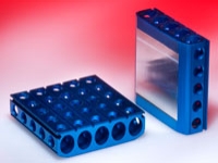
June 7, 2011 — JaroThermal’s Honeycomb heatsink directs heat towards the outside of the device, while Click to Enlargeproducing a steady flow of cool air inside the heatsink. Honeycomb heatsinks can be used with either plastic or metal/ceramic BGA packages, depending on the thermal interface material (TIM).

The design is studded with holes, helping increase surface area and cross ventilation. Ambiant air is cooled even as heat is released.

Applications include video cards, motherboards and networking applications. The design is thin, suiting compact, low-profile designs.

JARO’s adhesive mounted version eliminates the need for mounting holes in the PCB.

Jaro Thermal provides electronics thermal management technologies. Learn more about the product at http://www.jarothermal.com/honeycomb.pdf (PDF)

Click to Enlarge

Also read: Cooling high-power packages by Kaveh Azar, Ph.D. Advanced Thermal Solutions

Subscribe to Solid State Technology/Advanced Packaging.

Follow Advanced Packaging on Twitter.com by clicking www.twitter.com/advpackaging. Or join our Facebook group
June 3, 2011 – Marketwire — NXP Semiconductors N.V. (NASDAQ:NXPI) launched overmolded plastic package (OMP) RF power devices with 2.5-200W peak power. The plastic packages are a lower-cost option alongside NXP’s ceramic package RF devices.

The overmolded plastic package can reduce bill of materials (BOM) costs by 20% (compared to ceramic), said Mark Murphy, director of RF power products, NXP Semiconductors.

NXP’s OMP line covers these high-volume frequency ranges and applications:

  • 10 – 500-MHz ISM,
  • 470 860-MHz broadcast,
  • 700 – 2200-MHz GSM, WCDMA telecom,
  • 2300 – 2700-MHz LTE telecom,
  • 2.45 GHz ISM,
  • and products for the 2700 – 3500-MHz S-band.

NXP will package OMP products up to 10W using its existing IC packages; higher-power devices will be in new footprint packages. Gull wing packages will be available for surface mount assembly.

Product types will extend to existing categories: discrete pre-drivers (2.5-10W), drivers (20-45W), MMICs (20-60W), finals (50-200W) and integrated Doherty devices (50-110W). The plastic packages are available in ranges from DC to 3500 MHz; single-stage broadband drivers in HVSON, from 2.5 to 10W; single-stage drivers from 25 to 45W; dual-stage MMICs from 20 to 60W (high-gain drivers or combined as low-power dual-stage Doherty amplifiers), fully integrated plug-and-play Doherty PAs in a single package (50 to 110 W), and SOT502-sized, single-ended and push-pull final transistors ranging from 50 to 200W.

A limited selection of devices are currently available as engineering samples, with volume production scheduled to start in Q4 2011.

NXP Semiconductors N.V. (NASDAQ: NXPI) provides high-performance mixed-signal and standard products. Additional information can be found by visiting www.nxp.com.

Subscribe to Solid State Technology/Advanced Packaging.

Follow Advanced Packaging on Twitter.com by clicking www.twitter.com/advpackaging. Or join our Facebook group

Click to EnlargeIn an exclusive series of blogs, imec reports from its International Technology Forum (ITF) last week in Brussels. Els Parton, science editor, imec, shares Jy Bhardwaj’s (Philips Lumileds) points about LEDs costs improvements.
 
May 31, 2011
— LEDs currently appear in applications where performance — color, brightness, light quality — defines a compelling advantage over conventional light bulbs. A few barriers still stand between LEDs and mass adoption in illumination. "First, there is the cost (lumens per dollar) that has to decrease by a factor 10 if LEDs want to be competitive with conventional bulbs. This 10x cost reduction will be achieved by both performance and cost improvements. More in detail, this will be achieved by increasing the internal quantum efficiency (IQE) at high drive current, by improving the Phosphor conversion and by increasing the wafer size with yield and scale enhancement," Jy Bhardwaj, vice president technology R&D at Philips Lumileds Lighting Company, explains.

The second barrier to be overcome is light quality, states Bhardwaj. How do you achieve a consistent, controllable shade of white? An important research topic to tackle this problem is getting a good control of the phosphorous layer (density and thickness) in the LED stack. "Our company has come up with a new device architecture that enables this. It’s a thin film flip chip architecture for InGaN LEDs,"explains Bhardwaj.

Bhardwaj predicts that it will take another 3 years to achieve the desired 10x cost reduction. And by 2020, 80% of our planet’s lighting will come from LED.

Bhardwaj’s colleague Iain Black at Philips Lumileds recently spoke to Solid State Technology’s The ConFab audience about LED manufacturing improvements. Read his points about LED costs improvements via manufacturing here.

Els Parton, science editor, imec, and colleagues are blogging exclusively for Solid State Technology and its ElectroIQ.com partners from imec’s International Technology Forum (ITF) last week in Brussels.


Read more blogs from imec’s ITF:


Subscribe to Solid State Technology/Advanced Packaging.

Follow Solid State Technology on Twitter.com via editors Pete Singer, twitter.com/PetesTweetsPW and Debra Vogler, twitter.com/dvogler_PV_semi.

Or join our Facebook group

May 31, 2011 – STATS ChipPAC says it has widened its range of packaging configurations for its fan-out wafer-level packaging technology. Integrating through-silicon via (TSV) with integrated passive devices (IPD), on the company’s embedded wafer-level ball grid array (eWLB) platform, addresses complex designs, shrinking lithography nodes, and increased performance demands for mobile and consumer applications, according to the company.

Interconnecting through the silicon wafer surface (instead of around via wires) better utilizes space efficiency, improves formfactor, and improves electrical performance. Use of TSVs is particularly beneficial with passive devices, which take up a lot of space (up to 60%-70%) in a subsystem or SiP package.

Integrating the eWLB, TSV, and IPD technologies, "opens up a wide range of possible design configurations for SiP and 3D packaging at the silicon level," said Han Byung Joon, EVP/CTO of STATS ChipPAC, in a statement. "This is an effective approach to system partitioning which offers our customers an overall better system performance."

The company’s expanded range of package architectures includes single die, multi-die, ultrathin, system-in-package (SiP) and 3D packaging, with what the company calls "superior electrical and thermal operating characteristics."

Learn more about STATS ChipPAC at www.statschippac.com

Georgia Tech researchers have promoted an "all-silicon" packaging concept for several years, calling for integration of wafer-level and 3D stacking technologies to bring tighter node silicon, vertical die integration, and embedded passives together. Read about the idea in 3D Technology and Beyond: 3D All Silicon System Module by Ritwik Chatterjee, Ph.D., and Rao R. Tummala, Ph.D, Packaging Research Center – Georgia Institute of Technology

May 31 2011 — RJR Polymers, high-performance air cavity package (ACP) developer, will debut liquid crystal polymer (LCP) semiconductor packaging technology for RF and microwave system designers at the International Microwave Symposium (IMS2011). RJR’s new product is competitive with ceramic ACPs, improving thermal management and offering design flexibility based on the company’s epoxy range. 

The company is currently offering two thermally-enhanced, metal-based ACP platforms for radio frequency (RF) power and quad flat-pack no-lead (QFN) applications.

Designers can use copper or various other metal bases in the new package, selecting RJR’s epoxies and epoxy-coated lids to meet design-specific requirements. Thermally efficient power transistor packages need to handle higher-performance devices now, said Wil Salhuana, president and CEO, RJR, noting that designers still require flexibility for their systems.

The three-piece package can include materials with high thermal conductivity and components with higher co-efficient of thermal expansion (CTE) mismatch. The modular product line uses a standard molding process and creates a flat seal surface. RJR says this manufacturing technique creates one-third the dielectric found in ceramic and copper leads. By creating a single injection mold and simply swapping out the lead frame, LCP ACP users can use the same package for diverse products with lower design overhead and development time than creating new packages for each iteration.  The packaging technology can be built to all industry standard configurations or modified for custom designs.

RJR will be available to discuss this innovative packaging technology at IMS2011 in booth 718. The IEEE Microwave Theory and Techniques Society (MTT-S) International Microwave Symposium covers all of the latest developments in microwave technology from nano devices to systems applications, June 5-10 in Baltimore, MD.

RJR Polymers, Inc. develops air cavity LCP semiconductor packaging, epoxies, epoxy-coated lids and sealing equipment for RF, cellular, automotive, optical, imaging, and sensor applications, as well as new solar power, high-power LED, and highly integrated system-level applications. For more information, visit www.rjrpolymers.com.

Subscribe to Solid State Technology/Advanced Packaging.

Follow Advanced Packaging on Twitter.com by clicking www.twitter.com/advpackaging. Or join our Facebook group

May 26, 2011 — Ivo Bolsens, Xilinx, compares crossover cars — sports car performance with station wagon utility — to semiconductor ASICs (high-performance) and FPGAs (flexible, easy to use, less NRE). The semiconductor industry needs a programmable platform that has ASICs’ capabilities.

Bolsens continues, "An ASIC has typically a large non-recurrent engineering [NRE] cost," saying that 28nm chips need almost one hundred million dollars invested, and then must turn a profit. FPGAs are more expensive on a component-by-component basis, but have lower NRE. Crossover SoCs should bridge the gap between ASICs and FPGAs.

Bolsens finishes the interview with a focus on 28nm 3D chip architecture — particularly the confusion around supply chain handoffs. "There has to be a lot more agreement on roadmaps and standards so that all the players…have a good understanding of where investments should go." Right now, there are "a lot of opinions."

Bolsens knows what he’s talking about. In late 2010, Xilinx introduced 28nm 7 series FPGAs using 3D packaging technologies. They dealt with the turbulence of the young 3D packaging supply chain and process flows firsthand.

Research consortia can play a role in advancing 3D packaging, as can EDA providers, Bolsens asserts.

More from the ConFab:

May 25, 2011 — imec’s 3D integration industrial affiliation program (IIAP) partnered with Atrenta Inc., SoC realization products provider to semiconductor and electronic systems industries, to developed an advanced planning and partitioning design flow for heterogeneous 3D stacked ICs.

Cost-effective, rapidly ramping 3D ICs require robust, accurate partitioning and early prototyping. The flow imec and Atrenta are working on aims to minimize design iteration rounds. They demonstrated their first EDA tool flow for 3D design at DAC 2010. 3D stacked ICs reduce package footprint, and offer shorter and faster interconnects, possibly at lower costs. Stacked IC designs can be modular, and reused over various systems. The technology best suits mobile and high-performance applications, stacked DRAM, imagers, and solid-state drives.

The number of potential processes to resolve a given system design problem (e.g., front to front, front to back, silicon interposer, technology choice for slices, via configurations, partitioning, etc.) is huge. Creating multiple full design solutions for comparison is prohibitively expensive and time-consuming. Robust, accurate partitioning and prototyping early in the design process, well before detailed implementation begins, will avoid much of this trouble.

Other 3D design challenges include thermal profiles (heat dissipation) and mechanical stresses from assembly configurations. Imec has developed compact thermal and mechanical models for rapid generation of heat dissipation and mechanical stress maps and has validated them using real 3D DRAM-on-logic packaged devices. Atrenta’s SpyGlass Physical 3D prototyping tool creates design "floor plans," which can be combined with the stress models developed by imec, to compare options in different scenarios before full design implementation.

Imec and Atrenta will be demonstrating this flow at the Design Automation Conference (DAC) in San Diego, CA, June 6-8, 2011, in the Atrenta booth (1643). See design partitioning across a 3D stack with routing congestion analysis, through silicon via (TSV) placement and backside redistribution layer (RDL) routing support. The demo will also include a display of thermal profiles on the 3D "floor plan." For more information about Atrenta’s demonstrations at DAC visit: http://www.atrenta.com/DAC2011/sessions_short.html

Imec performs world-leading research in nanoelectronics. Further information on imec can be found at www.imec.be.

Atrenta provides SoC Realization solutions for the semiconductor and electronic systems industries. Learn more at www.atrenta.com

Subscribe to Solid State Technology/Advanced Packaging.

Follow Advanced Packaging on Twitter.com by clicking www.twitter.com/advpackaging. Or join our Facebook group

May 25, 2011 — Semiconductor packaging and die specialist Chip Supply Inc. in Orlando, FL, is changing its name to Micross Components, which Click to Enlargereflects the acquisition of Chip Supply last November by Micross Components in Los Angeles, CA. Micross provides specialist products and services for high-reliability electronics for high-reliability, industrial, and commercial applications.

Chip Supply, which provides interconnects on bare die, chip scale packaging (CSP), and multi-chip modules (MCM) has begun using the name Chip Supply Inc., doing business as Micross Components, and eventually will drop the Chip Supply name altogether, says Alan Taylor, chief executive officer of Micross.

Operations at the Chip Supply Orlando facility, which has 150 employees, five buildings, and 42,000 square feet of processing space, will continue as before the acquisition, and Orlando will become the base for all Micross die business in the United States.

Micross executives are consolidating the company’s Fairfield, NJ, operations in Orlando. Eventually the company will consolidate its operations in Austin, TX, at the Orlando site as well.

The Micross facility in Hatfield, PA, will continue operating as the company’s main US site for all Micross interconnect products and component modification services.

The Chip Supply operations in Orlando provide semiconductor interconnect, test, and assembly services. The Orlando campus has 10,000 square feet of cleanroom space in two cleanrooms, as well as wafer-processing and -encapsulation equipment for post-wafer fabrication semiconductor processing. For more information contact Chip Supply online at www.chipsupply.com, or Micross Components at www.micross.com.

Originally posted by John Keller of Military & Aerospace Electronics

May 24, 2011 — Carsem, turnkey semiconductor packaging and test services provider, will grow its Suzhou, China factory by an additional 40,000 square meters (430,000 square feet). The additional space will allow Carsem to increase their Suzhou factory micro leadframe package (MLP) capacity from the current 5 million units per day to over 20 million per day, with a focus on copper wire bonding.

Click to EnlargeConstruction commenced in Q1 2011 and production operations are expected to begin in Q1 2012. The expansion will bring the total factory size to 56,000 square meters (600,000 square feet), with expanded test capability to match the new production output. Carsem expects to attract new potential customers with the capacity boost. 
The added assembly space will allot for increased copper wirebonding, along with traditional gold wire bond. Several packaging houses are moving to copper wire bonds for increasingly complex packages. MagnaChip Semiconductor now offers cost-competitive and state-of-the-art copper wire bonding technology and STATS ChipPAC Ltd. (SGX-ST: STATSChP) is investing in Cu wire bonding for finer silicon nodes (45/40nm) and low-k/extra low-k (ELK). Opponents consider gold wire to perform better than Cu wire, citing in-service product reliability, process yield, and "unproven performance."

Once completed, the Suzhou expansion will bring Carsem’s total MLP manufacturing capacity in both their Ipoh, Malaysia and Suzhou, China factory locations to over 26 million units per day.

Carsem MLPs are quad flat pack no-lead (QFN) and small-outline no-lead (SON) packages complaint to JEDEC MO220 and MO229 standards and are also offered with enhanced technologies such as copper-clip, flip-chip, system-in-package (SiP) and the 0.3mm-thick X3 form factor.

Carsem provides turnkey packaging and test services to the semiconductor industry, and offers a wide range of package & test services. Visit the website: www.carsem.com.

Subscribe to Solid State Technology/Advanced Packaging.

Follow Advanced Packaging on Twitter.com by clicking www.twitter.com/advpackaging. Or join our Facebook group

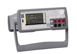
May 24, 2011 – BUSINESS WIRE — Agilent Technologies Inc. (NYSE:A) released the B2900A Series line of compact benchtop source/measure units (SMU) for semiconductor, component, and materials testing. The company claims that these SMUs offer capabilities competitive with semiconductor device analyzers.

Click to Enlarge

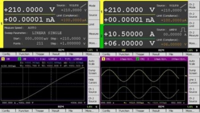
These SMUs provide wide voltage/current ranges with a graphical user interface (GUI) on color displays. For an entry-level cost, the SMUs provide current-versus-voltage (I-V curve) characterization on semiconductors, active and passive packages and materials. Users can perform interactive testing, debugging and characterization faster than on conventional SMUs, according to the company. Under programmatic control, the new SMUs support the SCPI command set, enabling migration from conventional SMUs, and basic compatibility.

Click to Enlarge
Figure. The Agilent B2900A 4.3" color LCD display supports graphical and numerical view modes, and enables test set-up and check test results quickly. Single view, dual view, graph view and roll view improve usability and productivity of bench-top test, debug and characterization.

Agilent expects research and development (R&D), manufacturing and education customers for the line.

The B2900A Series comprises four models: the B2901A and B2911A (one-channel) and the B2902A and B2912A (two-channel). The line features:

  • ±210V voltage range
  • ±3A DC and ±10.5A pulsed current ranges
  • 100nV and 10fA minimum resolution
  • 12,500 readings per second (maximum sweep-operation reading rate, source/measure to GPIB) archived.

An SMU integrates voltage/current sources, voltage/current meters, switches and arbitrary waveform generator capabilities for easier, simpler characterization and device analysis. Many Agilent SMUs, including the B2900A Series, can operate as a four-quadrant voltage/current source, an electrical load, a voltage/current meter, a pulse generator and an arbitrary waveform generator without changing connectors or tools. The new line complements Agilent’s B1500 semiconductor device analyzer, the N6700 modular power system and the N6705 DC power analyzer.

Agilent Technologies Inc. (NYSE: A) provides measurement technologies to chemical analysis, life sciences, electronics and communications industries. More information about the B2900A Series is available online at www.agilent.com/find/B2900A.

Subscribe to Solid State Technology/Advanced Packaging.

Follow Advanced Packaging on Twitter.com by clicking www.twitter.com/advpackaging. Or join our Facebook group