Category Archives: LEDs

(July 1, 2010) — Ariadne announces a new collaboration with the BIO-NMD consortium led by Professor Alessandra Ferlini at the University of Ferrara, Italy. BIO-NMD is a three year, 7.5M€ EU-funded medical research project concentrating on the search for non-invasive biomarkers in people with Duchenne and Becker muscular dystrophies and Collagen VI myopathies. The consortium, along with leading European academic research and industry partners will work to identify non-invasive biomarkers for monitoring neuromuscular diseases (NMDs). Utilizing a myriad of OMIC sciences (genomic, transcriptomic, proteomic) and bioinformatics, the consortium hopes to bring qualified biomarkers for ongoing and further clinical trials.

Ariadne’s focus will be on providing bioinformatics tools for identifying functional pathways, potential targets and data outflow integration. The team will use its software, Pathway Studio®, as a core to integrate the data and information flow, in addition to using its expertise in information extraction to develop a literature-derived NMD biological knowledgebase of related processes and diseases. Specifically, Ariadne will build mechanistic models and pathways for NMD and interpret OMIC data generated by the consortium and partners in the context of NMD knowledgebase and networks.

BIO-NMD’s coordinator and chair of the steering committee, Professor Alessandra Ferlini (University of Ferrara, Italy) said, “The participation of Ariadne as partners together with INSERM is crucial for the project. Developing bioinformatic tools for OMIC studies analysis is essential and guarantees success to the project. In addition, it reinforces collaboration between academics and industries, again a key point for successful research to be translated into clinics.”

“We have always worked to establish strong collaborations with our clients”, says Gabriella Armin, Director of Marketing for Ariadne. “Given the importance of this project, we are proud to not only provide the technology to enable this type of innovative discovery research, but contribute scientifically as team members. Our technological expertise in knowledge enrichment continues to provide crucial bioinformatics tools for visualizing the complexity found in biology.”

The first update workshops for the BIO-NMD consortium are to be held in July in London and will include sessions dedicated to its industrial partners. The consortium will present and describe the project impacts, possible outcomes and identify links for future collaborations with industry. For further details about the project please visit the BIO-NMD website at www.bio-nmd.eu

Ariadne (www.ariadnegenomics.com), a leader in research data products and knowledge enrichment-based software solutions, helps pharmaceutical and life science researchers tap known scientific knowledge for applications in systems biology and translational medicine. Products include custom data products, knowledge extraction and visualization software, knowledge reports, and informatics staffing.

BIO-NMD (www.bio-nmd.eu) is an EU-funded project devoted to the discovery and validation of biomarkers in muscle dystrophies with the aim of improving disease and therapy monitoring. It is a translational project which will focus on Duchenne and collagen VI myopathies. The project is a consortium of 12 partner institutions led by the University of Ferrara’s Prof. Alessandra Ferlini, funded until Dec 2012.

Read more about Nanotechnology in Medical Sciences

Read more about University Research

(July 1, 2010) — Inspired by the ease with which gecko lizards can move on almost any surface, researchers at Northeastern University, the Korea Institute of Science and Technology and Seoul National University hope to reproduce properties found in the gecko’s footpad for applications ranging from adhesives to robotic movement and navigation.

The team, led by Ashkan Vaziri, assistant professor of mechanical and industrial engineering at Northeastern; and Myoung-Woon Moon, of the Korea Institute of Science and Technology, created nanoscale and microscale patterned surfaces with adhesion and friction properties similar to that of the gecko footpad.

Asymmetric adhesion is used by many insects and gecko lizards, allowing them to move on nearly any surface – horizontal, tilted or vertical. Many of these creatures have feet covered by intricate fibrillar structures that are responsible for their superb climbing ability. Among these creatures, gecko lizards have one of the most efficient and interesting adhesion devices consisting of finely angled arrays of branched fibres (setae). Gecko toes are covered by millions of hair-like setae, each of which is five micrometers in size — smaller than a human hair. The ends of the setae are tipped with hundreds of spatula, which bend and conform to the surface on which the gecko is moving.

The innovative nanotech methodology, published online and in the academic journal Soft Matter, could lead to the development of a “smart” adhesive that adapts to environmental stimuli, such as a curvy surface or a rough edge.

“The gecko footpad’s unique structure and function make it one of the most efficient adhesion systems found in nature,” said Vaziri, who also directs Northeastern’s High Performance Materials and Structures Laboratory.

The research team designed and created a series of micropillars, or hair-like structures, and exposed them to ion beam radiation. The radiation tilted the micropillars, resulting in a dual-surface area with unique adhesion and friction properties. 

Through a series of experiments, the team found that the micropillars had qualitatively similar friction properties and function when compared to the gecko footpad.

“If equipped with micropillars, small high-tech robots (for research or military applications) might be able to climb with speed, precision and accuracy on uneven, slippery surfaces,” said Vaziri.

The technology also could lead to a new generation of smart adhesives that are equipped to hold strong bonds with any surface, he said. The polymer micropillars don’t yet have the hierarchical structure found on a gecko’s setae. This is something the team hope to replicate in the future.

Read the Journal article in Soft Matter here.

Read more University research announcements here.

In the future, the production of advanced LED structures is expected to grow more rapidly with the growth in energy efficient, long-lifetime luminaries for general lighting applications. In this article, we will outline the most important measurement capabilities that allow the rapid and reliable control of the LED production process using HRXRD, and the latest advances in HRXRD technology to allow true in-line monitoring. This article includes a video interview with Jordan Valley Semiconductors from SEMICON West 2010.

Paul Ryan, John Wall, Richard Bytheway, David Jacques, Kevin Matney, Qu Bo, Jordan Valley Semiconductors UK Ltd, Belmont, Durham, UK

Key parameters for the quality of advanced LEDs are the wavelength and brightness of the emitted light. Several structural parameters control these aspects, and these have traditionally been determined using high resolution X-ray diffraction (HRXRD).

A typical HB-LED structure is based on III-nitride materials and is dominated by a repeating unit of InGaN and GaN layers. These two, thin layers are repeated several times (typically between five and 10 repeat units) to create a multi-quantum well (MQW). This MQW is the heart of the LED structure, and the details of the MQW structure determined using HRXRD play a key role in the success of the device. In particular:

1. The In composition within the InGaN layer, along with the number of repeats within the MQW, the wavelength of the light can be controlled;

2. The repeatability of the thickness of each layer within the stack is critical for efficient MQW structures; and

3. The mosaic tilt and twist of the structure controls the efficiency and yield of the device

In this video from SEMICON West, Isaac Mazor, Jordan Valley Semiconductors, talks about LED structures and the LED market: the green/eco drivers, high investment in capacity, energy savings, etc. LED applications go side-by-side with semiconductor fab applications.

Measurement of In composition and MQW thickness

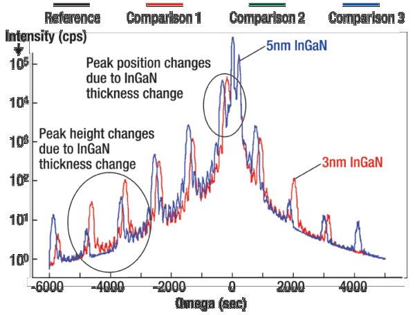
A perfect LED structure, with a MQW repeat of 15nm and a 15% In composition, would give a HRXRD pattern as shown in Fig. 1. The general diffracted intensity consists of a narrow, intense peak from the GaN buffer layer (centered at 0s in the figure), another peak to slightly higher angle of the GaN, which is attributed to the AlGaN layer. The position of this peak is related to the Al content within the AlGaN layer, and the height, and width, of this peak is related to the thickness of the AlGaN layer.

Click to Enlarge
Figure 1. The effect on the HRXRD spectrum by varying just the InGaN layer thickness.

The series of peaks from the MQW structure give a large amount of information about the layer thicknesses and composition within the MQW:

1. Satellite period gives the combined thickness of the InGaN and GaN (bilayer repeat thickness); and

2. The position of main MQW peak gives the average In composition within the InGaN / GaN pair (note, this is not the In composition within the InGaN layer).

To determine the actual In composition within the InGaN layer, a number of other factors must be considered, namely the individual InGaN and GaN layer thicknesses within the MQW, and the relaxation of the MQW structure relative to the GaN buffer layer. We will consider the case where the layers are assumed to be relaxed, as is often historically assumed within production.

There are two main affects on the data when the InGaN thickness is changed, as shown in Fig. 1. First, the MQW to substrate peak separation increases, as the average composition within the MQW has increased by increasing the InGaN thickness relative to the total GaN + InGaN thickness. Second, the period of the satellite peaks remains unchanged, but the ratio of peak heights varies with the InGaN thickness. Therefore, to enable the InGaN layer thickness, and hence the In composition, the data must cover several satellite peaks and the simulation software must accurate fit to the satellite peaks over a wide angular range. It should be apparent that a high intensity incident beam and low baseline is required in order to reliably determine these key structural parameters.

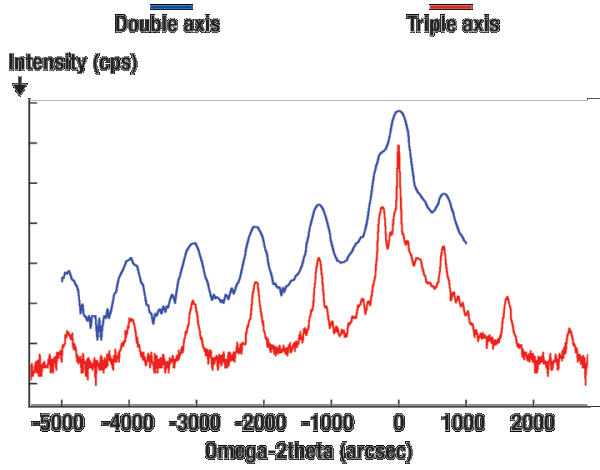
In the examples above, the structures are assumed to be structurally perfect. However, the growth of GaN is typically dominated by a mosaic structure. This mosaic structure has a major influence on the HRXRD spectrum. The peaks are broadened as the mosaic tilt essentially smears out the details of the diffraction pattern. This leads to the main MQW peak being merged into the main GaN peak, as shown in the blue spectrum in Fig. 2, preventing accurate analysis of the In composition. However, the data is still suitable for bilayer thickness analysis.

Click to Enlarge
Figure 2. Comparison of HRXRD spectra collected with and without triple axis analyzer crystal, from an MQW structure with mosaic tilt.

To enable accurate and precise measurements of the key MQW parameters the influence of the mosaic tilt must be minimized within the HRXRD data. This is achieved by inserting an analyzer crystal in front of the detector in order to improve the angular resolution of the measurement without substantially reducing the intensity. This then allows high-quality diffraction data to be obtained, as seen in the red spectrum (Fig. 2). Advances in X-ray measurement techniques allow these measurements and automated analysis to be performed in a few seconds on production HRXRD monitoring systems, such as the QC3 tool.

Traditionally, HRXRD has often been used for process development applications using a traditional R&D diffractometer, typically requiring a manual configuration of the system with long data collection times and tedious analysis of the data. However, dedicated production optimized HRXRD systems are now available that have specifically designed to address many of these issues at a low cost of ownership. The QC3 system, for example, allows triple axis scans to be performed in less than one minute. It allows for automated configuration of the system, wafer alignment and full structural analysis in parallel with subsequent measurements. Results can be output in a variety of formats and customized for statistical process control SPC.

Conclusion

For the accurate determination of In composition, and hence wavelength, high quality diffraction data with high intensity, low background that span wide angular ranges are necessary, and full dynamical simulation is required for detailed analysis. This requires a high intensity source with a high dynamic range detector.

The latest generation of HRXRD tools specifically for production monitoring are designed to be able to determine the key structural parameters for LED analysis on multiple wafers in a single batch run, with a simple user interface suitable for a production environment.

Biographies

Paul Ryan received his BSc and PhD from the U. of Leeds, UK and is VP Corporate and UK Site Manager at Jordan Valley Semiconductors UK Ltd, Belmont Business Park, Belmont, Durham, UK; ph.: +44 191 332 4700; email  [email protected].

John Wall is R&D Manager at Jordan Valley Semiconductors UK Ltd.

Richard Bytheway received his BSc from the U. of Wales, Swansea, UK and is a technologist at Jordan Valley Semiconductors UK Ltd.

David Jacques received his D.E.A and Diplome d’Ingénieur from Institut National des Sciences Appliquées de Toulouse and is a product manager at Jordan Valley Semiconductors UK Ltd.

Kevin Matney received his BS and MS from UCLA and is a senior technologist at Jordan Valley Semiconductors Inc.

Qu Bo received his PhD from the Institute of Semiconductors, CAS and is a regional applications manager for Asia at Jordan Valley Semiconductors UK Ltd.

More Solid State Technology Current Issue Articles
More Solid State Technology Archives Issue Articles

June 25, 2010 – A three-day event put on by the Center for High-Rate Nanomanufacturing (CHN), one of four US nanomanufacturing centers and a collaboration of regional institutes (U. of Massachusetts/Lowell, Northeastern U., and the U. of New Hampshire), offered insights and updates on all things nano, from self-assembly and measurement techniques and requirements to applications in batteries, photovoltaics, and sensors.

Thomas Russell of UMass/Amherst discussed bottom-up self-assembling block copolymers, with the highly directional field & mobility of solvent, to create "perfect" hexagonally packed arrays (3×3 cm2) area, and areal densities of -10.5 TB/in2 — the equivalent of ~25 DVDs, he said. One problem: "the industry can’t write to it, and can’t read to it!" He suggested the data storage industry will have to push further into SSDs, though this will mean having to "push the limits" of etch and evaporation processes — e.g., etching along a crystal’s surface and controlled directionally. His team has not yet made such a high-density device, he noted.

JA Liddle from NIST looked at measurement challenges with the need to find a functional sweetspot of defectivity, high throughput, and tiny size. Measuring for "fundamental understanding" is too slow, expensive, and infrequent — but measuring for "process and quality control" is fast, cheap, and offers periodic/continuous results, both offline and in real time. He led this discussion into understanding more about self-assembly, which has limited control except for setting boundaries. Diblock copolymers can put small features close together, but measuring line-edge roughness with SEM looks "terrible," possibly because of damage caused by the technique itself. Resonant x-ray scattering, which can measure interfacial width/roughness to sub-0.5nm accuracy, he called "a lot more encouraging," and it can also be used for sidewall angles. For roll-to-roll diblock copolymers, techniques must be specific to the type of pattern being measured, and models must be developed for data extraction. A laser gauge sensor, he pointed out, looks a lot like a spinning HDD — so it’s feasible, he said. To follow the behavior of a single molecule, where Brownian motion limits dwell times, Liddle suggested tracking fluorescence correlation spectroscopy (FCS).

One challenge in measurements: morphological diversity in CNTs (single-walled, multiwalled, double-walled), which depend on finding the right combination of catalyst, temperature, precursor, pressure, etc. For now, measuring both process control and quality control (end-of-line) is "a really good problem statement," he said. Invoking the rule of "maximum laziness," he suggested defect location could be as simple as thermal examination (e.g., to find a short between two films, as in a PV application), but for a single pixel out of alignment, "near-field is the only chance."

Continuing on the CNT theme, David Arthur from CNT supplier Southwest Nanotechnologies (SWeNT, one of the event’s sponsors) noted the price/demand differences between the different types of CNTs. Multiwalled nanotubes are available in hundreds of tons/year, from lots of suppliers, at prices as little as $0.05/$0.50/g, for more general bulk applications. Single-wall nanotubes, meanwhile, are relegated to mainly niche coating applications due to their low volumes/availability and related high prices ($50-2000/g). But there’s an emerging opportunity in between, he said, that SWeNT wants to tap: specialty multiwall nanotubes (~3-6 walls), with better properties than normal MWNTs (e.g. easier to disperse, high ~10,000:1 aspect ratios), priced somewhat cheaply )$0.50-$50/g). SWeNT has ramped its output of CNTs to about 1kg/day, and plans to scale to 1 ton/day by 2012, while reducing costs by 10x. (He noted that the company’s products well exceed — though not with precise determination — industry standards (e.g., 90% semiconducting and 40% type [6,5]). Targeted applications include a CNT ink printable using standard manufacturing equipment, and printed LED lighting. Another key area is in new cathode materials for Li-ion batteries that meet cycle/life, low-weight, and cost needs. Initial data Arthur showed from RIT suggests comparable metrics to conventional cathode materials — same profile discharge, but better across cycling. Arthur also described fiber-reinforced fabrics (dipped in a CNT solution) for use as structural sensors, taking advantage of a correlation between measurable mechanical strain and conductivity. Such fabrics are already installed in two bridges in Alabama, he noted.

Asked about the biodegradability of CNTs — EHS is a critical concern with nanomaterials, and took up an entire day’s worth of presentations at the nano event’s first day — Arthur acknowledged that they are "likely to have a pretty high persistence in the environment," and the best approach may be to rely on encapsulation to "minimize their release."

Returning to self-assembly themes, Joey Mead of UMass/Lowell explained directed self-assembly with polymers, where current work emphasizes determining the effectiveness of the template and polymer blends. These blends can be assembled in 30sec with no anneal and in uniform patterns (e.g., 90o, T-junction, circle and square arrays). Patterning multiple length scales is possible, with 100-300nm spacing on a single template — her team wrote "CHN" using polymers (the name of the joint nano center). Key is knowing the interdependence and thus sweetspots of three factors: domain size, spin speed, and concentration. As an example, domain size and pattern pitch should be within 10% of each other. Mead also discussed work in transferring CNTs from a surface (e.g. PDMS stamp) — the opposite of what the previous speaker from SWeNT would want! — using a type of thermoforming similar to making yogurt cups: heat a polymer sheet, put the template into the base of the mold, and push it up to transfer. This works for conducting polymers as well as CNTs, she noted.

Tom Van Vechten, representing NanoComp (another event sponsor), talked about CNTs’ synthesis and application in thermoelectrics, where change in temperature is utilized to create electricity. (In cars, 44% of fuel is exhausted through the radiator, equivalent to ~10s of kW, he noted.) He discussed putting n-type and p-type semiconductors in series, and the company’s creation of a flexible CNT "felt" as an alternative generator material vs. typically Bi2Te3 — but as comparative numbers showed, there’s a very long way to go. "We have ideas about how to continue" the progress of CNT felt material, ultimately targeting $1/W in five to seven years. Possible application would be taped to the back of a solar collector to increase overall system output.

Morphology was the main topic of discussion for Konarka’s Eitan Zeira, as the company works to increase PV efficiency with a new polymer structure, and devising morphology is the main challenge for spontaneous phase separation and making polymers that stack up quickly. Efforts with PCBM only show up to 6% efficiency, he noted.

Another take on nano in PV was offered by Loucass Tsakalakos of GE Global Research Center, who talked about the group’s work on nanowire solar cells, which promise "excellent optical properties" (better than planar/solid thin film), angular dependence, and can be doped n- or p-type. GE developed the nanowire process flow from scratch, he noted. Asked how to apply back contacts to such a nanowire array, e.g. on a low-cost metal foil, he explained that there "a lot of considerations," e.g. developing different barriers, but they can grow the NTs on a 4-in. stainless steel metal foil. Another issue is depositing a uniform coating, i.e. with PECFD for SiO2. More work is needed to model, for example, electric fields, the effect of gas transport on the wires, etc. A prototype a-Si device initially showed just 1.2% efficiency in first tests, but he hinted that new results forthcoming later this year will show ~11%, using compound semiconductor devices — comparable to organic & inorganic PV materials.

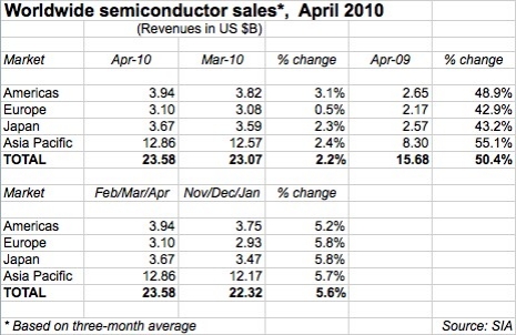
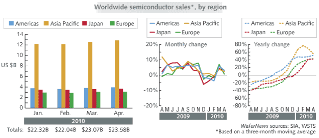
June 1, 2010 – Global semiconductor sales rose 2.2% in April to a new record high of $23.6B as the industry continues to march back from a bruising downturn, and is on track to settle back into seasonal patterns again, according to the latest monthly data from the Semiconductor Industry Association (SIA).

Chip sales (a three-month moving average) rose 2.2% from the previous month (March), and were up 50% from a year ago, which is just as much of a commentary on how lousy early ’09 was. Similarly, sales through the first four months of 2010 are up 54% from the same period in 2009. This continues similar growth seen in the first three months of the year, a quarter in which IC shipments peaked at a record 44.5B units. Note that the year-on-year comparisons are starting to look a little less jagged than in prior months — this is both due to improved comparison months (i.e., the industry improved in mid-2009 onward).

By region, the Americas continues to lead the charge, though Asian regions are right along with it. Even Europe managed to eke out monthly growth. Compared with a year ago, all regions enjoyed at least 43% growth, led by Asia-Pacific.

Click to Enlarge

Semiconductor sales growth (in dollar terms) is partly due to the resurgence of memory, where pricing has greatly improved. Deutsche Bank’s Ross Seymore, who is maintaining his 25% growth forecast for 2010, notes in a research report that minus DRAM, annual growth comparisons slip a bit to 40% (vs. 48%), as ASPs "remain solid." He also sees positive signs in month/month comparisons for MPUs and analog, both of which saw sales decline (-28% and -3% respectively) on weaker units, but less than historical averages.

Click to Enlarge

Credit Suisse’s John Pitzer downplays the significance of handicapping early-year growth trends, particularly this year with Euro troubles complicating things — and in fact the next few weeks (mainly June) are key. Minus memory, May and June should well surpass historical trends of barely 1% sequential growth, he says; if the rest of the year slides back into seasonality the year would close at about 29% growth, above consensus forecasts.

"While bears continue to be concerned that semis have outgrown end demand on a q/q basis over the past several quarters, we would highlight that IC unit shipments (ex-memory) remain 8% below long-term shipment trends," he notes. Barring significant double-dipping trends, "we suspect 2H10 numbers are still wrong and too low, especially if cyclical and structural supply constraints leads to better pricing," he writes.

May 10, 2010 – The Asys Group say it has acquired the IP and patents of fellow German firm DynTest Technologies, seeking to apply the company’s wafer singulation technology to high-brightness LEDs.

DynTest’s core technology is in wafer singulation for compound semiconductors and other substrate materials. Asys says it sees particular affinity in LED manufacturing, where DynTest’s technology is "a cost-efficient alternative to the saw-dicing and lasering methods." The company also points to synergies with DynTest’s technology’s improved wafer area utilization, and Asys’ depaneling systems for electronics systems, and metallization process lines for solar cells.

Development of existing prototype machines will be completed and ushered into mass production, with products already slated for release in 2010, the company says. The DynTest product line will be housed in Asys’ solar and new technologies business unit and directed by former DynTest sales/marketing exec Helge Luesebrink.

April 27, 2010 – The Extreme Ultraviolet Lithography System Development Association (EUVA) says it has surpassed 100W output at intermediate focus for an EUV light source, another big step to address a big hurdle facing EUV lithography as a production-viable candidate for next-generation semiconductor manufacturing.

Led by members Gigaphoton and Komatsu (Gigaphoton was formed in 2000 by JV parents Komatsu and Ushio), the mark of 104W power output at 2.5% conversion efficiency utilized a 7.9kW CO2 laser radiated onto a 60μ-dia. Sn droplet target; magnetic fields were used for debris removal. To hike the power output to the ~180-200W expected to be required for full volume manufacturing will require further increasing the CO2 laser output and improving the conversion efficiency. The EUVA says this laser-produced plasma (LPP) source should scale to >200W in-band power at intermediate focus, using a 20kW CO2 laser.

In a statement, Gigaphoton president Yuji Watanabe said the company would start ramping operations this quarter in its facility toward initial volume production, with shipments of EUV light sources slated for sometime in 2011.

At this year’s SPIE, Cymer said its EUV source had topped 90W at raw output, though this was significantly reduced at the intermediate focus; its source roadmap, though, predicts 200W by 1H11 and 350-400W within two years.

The EUVA is also pursuing another EUV source alternative — work led by member XTREME in Germany has put together a discharge-produced plasma (DPP) source eyeing 115W at intermediate focus, with conversion efficiency of 3.5% (about 1.5× better than conventional values, the EUVA says).

by Neha K. Choksi

March 31, 2010 – Displays are a hot topic, especially in the mobile consumer electronics industry. LCD displays are prevalent in today’s handheld devices, but their poor power efficiency and readability in bright light give incentive to uncover alternative approaches. Qualcomm senior engineer Rashmi Rao shared the company’s MEMS-based approach to displays at the IEEE Bay Area Nanotechnology Council meeting on March 16, 2010.
Click to Enlarge
Handheld devices are being used more and more during each day, which has large implications on the battery life of a device. Pike Research predicts that by 2014, 54% of cell phone battery life will be used toward displays. The current trend to address the issue has been to use heavier, thicker batteries, but Rao questions whether this is the true solution. Qualcomm’s mirasol display approaches the issue by trying to reduce the power consumption rather than increase battery size — an approach inspired by nature. Butterfly wings are made of millions of nanostructured etalons (two parallel reflecting surfaces). When light passes through the wing’s multilayered surface, it reflects multiple times, which leads to the intense, iridescent color for which butterfly wings are known.

Mimicking the butterfly, the company approaches a low-power display solution by creating a MEMS etalon device (see figure below). The top layer of this two-layer device is a partial reflector; the bottom layer is a total reflector. By defining the gap size between the two layers, the resulting reflected color can be specified. The bottom layer of the MEMS etalon is a moving membrane; thus the gap between layers can be modulated. The device operates as a bistable capacitive/electrostatic switch. The bright, open state is achieved by a low constant bias. By superimposing a short positive pulse, the movable bottom layer collapses for the "closed" state. The collapsed membrane results in an interference pattern of light that is not visible or "dark" to the viewer. This closed state is maintained until another pulse "un-writes" the device and the lower membrane moves back to its initial open state.

Because the device maintains its state unless pulsed, it is able to achieve lower power consumption than LCD and OLED display technologies that dominate the market today. Furthermore, Rao explains, the display is able to achieve a faster refresh rate and is also lighter than current displays. The device’s response time, on the order of microseconds, indicates that it is well suited for video applications. Also, color filters that reduce brightness in LCD technology are unnecessary for the MEMS-based display.

Click to Enlarge

Brightness is a key differentiator for this display in yet another way. Because the intensity of current display technology is limited by the illumination source, which cannot compete with the intensity of sunlight, LCD and backlight OLED displays are difficult to read in bright sunlight. But since the mirasol MEMS display depends on ambient light for its light source, it has an inherent mechanism for adjusting its brightness to its surrounding light intensity, lending itself to bright light conditions. In fact, the company claims excellent contrast: 90% reflected light in the open state vs. 1% in the dark state. Plus, by utilizing ambient light, the new product eliminates the need for backlight illumination and further reduces power consumption.

On the other hand, in darkened rooms or at night, the ambient light may be insufficient for these MEMS-based displays to reflect. Hence, is Qualcomm exploring the option of frontside illumination for low ambient light conditions. It is unclear what impact the frontside illumination will have on battery life, but the aim is to keep power usage well below current LCD and OLED technology.

When asked about reliability, Rao explains that a universal usage model is still < in the industry, thus complicating a metric for comparison to other devices. The company has conducted initial accelerated lifetime tests on the device in the operational temperature range, with and without humidity, but additional investigations are underway.

Despite work to be done, the new device has received significant attention — the display technology is targeted for the e-book market. Just as cell phones are demonstrating the intersection of technology with the Internet, cameras, gaming, TV/video, contacts, music, calendar, email, and more, Qualcomm’s MEMS displays have opportunities that can reach far beyond its initial entry point. But MEMS are just one of many approaches to next-generation mobile displays, and the company is not alone in pursuing a MEMS-based approach. As Rao states, "convergence is inevitable," and the company hopes to be on the front line as the push for energy efficiency continues.


Neha K. Choksi is an independent consultant based in Mountain View, CA. She has worked for a variety of MEMS companies including as director of product engineering at Silicon Microstructures and as independent consultant for SmallTech Consulting. E-mail: choksi [at] gmail.

March 26, 2010 – TSMC has officially broken ground for its new LED lighting R&D center and fab in Taiwan’s Hsinchu Science Park, part of its multibillion-dollar initiative to establish a foothold in higher-growth markets outside of core IC fabrication.

"LED lighting is a promising industry, and we will make full use of TSMC’s technology leadership and manufacturing excellence in semiconductors to develop and integrate LED technology, process, and packaging and testing," said Rick Tsai, TSMC’s president of new businesses. The company plans to enter the market in 2011 with LED light sources and "light engines," he added.

The new facility will be built in two phases, TSMC says: Phase 1, with a NT$5.5B/US ~$173M investment, projects equipment move-in for 4Q10 (including 8-12 MOCVD chambers, according to the Taiwan Economic News) and anticipating a production ramp in 1Q11.

A second phase will be decided depending on the market and "future business needs." The company says it is "actively recruiting" for the business, in all areas: technology development, process integration, product mechanical engineering, packaging and testing, equipment engineering, facilities, and business development. TSMC already has been adding packaging/testing capabilities through subsidiaries Xintec and VisEra Technologies to facilitate integrated production, adds the Taiwan Economic News.

Last summer TSMC brought back former leader Morris Chang to retake the helm (from Tsai) and expand its leading-edge semiconductor technology out into the world, particularly into LEDs and solar energy, creating up to $2B in nonfoundry business by 2018.

Rival Taiwanese foundry UMC also has eyes for the LED market; it plans to set aside ~20% of its 150mm fab for LED epitaxy wafers, and add work for LED packaging/assembly at a site in China.

March 15, 2010 – A year after calling a new deal with TSMC to make some of its Atom processors "an important step in a long-term strategic technology cooperation", that partnership apparently has floundered — and it’s a good example of the complex battles the top chipmaker is trying to fight, according to one analyst.

The deal announced in March 2009 ported the Atom processor CPU cores (including IP, libraries, and design flows) to TSMC, in an attempt to help broaden its appeal as a system-on-chip (SoC) for mobile devices — a move interpreted as a stab at the heart of ARM’s market. TSMC reportedly shifted its MPU lines from facilities in northern Taiwan to southern Taiwan and added backend tools, anticipating the work to contribute 1%-2% of 2010 revenues; some analysts have suggested upwards of $1B in annual business from 2011.

But a story from the New York Times reveals that the collaboration is now "on hiatus", though an Intel exec says it’s not officially ended.

CNet’s Tom Foremski more specifically points out ARM’s advantages in a war with Intel (large design library, low-poer and smaller design attractive for mobile apps, large installed base with smartphones and resultingly legions of developers familiar with its capabilities), though "Intel certainly has the talent and resources to make future Atom designs that are competitive with ARM in terms of power consumption and size."

However, Gary Smith from GarySmith EDA suggests that the Intel/TSMC/Atom deal wasn’t just put on hiatus because of slow customer demand — "it was a bad idea to begin with," and TSMC was the only party who would have gained. "By trying to mimic the ARM model, Intel would have only cannibalized their own revenue stream," he writes in a new research note. Trying to be a fabless vendor (for Atoms & mobile apps, competing against ARM) won’t work, he says; while Intel can compete with ARM technically, "they can’t compete commercially […] they have to compete with ARM’s customers" in various markets, and "trying to take on everyone would led to disaster." Meanwhile, its pedigree as an IDM (for its PC and server business, competing against the likes of IBM) puts them on top only in certain areas where resources can be focused and profits can be made — that means the biggest markets like PCs and servers, "so they definitely are less maneuverable than their competition," he notes.

Ultimately, Intel has to do what it has continued to struggle with — find ways to deeply understand emerging markets, then attack with the same skills it used in dominating PCs. "They are not going to win them all but they certainly need to win the majority of those they target," Smith writes. "ARM will still dominate a majority of the markets," he notes, but Intel needs only "to dominate enough of the largest markets so they can maintain their critical mass as an IDM."