At the Confab, Bill McClean, president of IC Insights, tells SST‘s Debra Vogler that ASPs are still holding and it will take the industry some time to build up its capacity.
Category Archives: Uncategorized
Aart de Geus of Synopsys describes what he sees as an industry shift to "systemic collaboration," enveloping all the areas of today’s and future leading-edge semiconductor systems, from node-scaling to power management to embedded software. Fewer companies can do all of it on their own — so orchestrated collaboration is becoming a core discipline, and a key differentiator.
In a video interview at The ConFab, SanDisk founder/president/CEO Eli Harari expands on two themes in his Monday keynote address: the precise timing of new fab investments to promote a healthy supply/demand balance, and what it will take to get to the "post-NAND" world.
by Pete Singer, editorial director
May 19, 2010 – Look for strong growth in the second half of 2010 and several years of continued growth, said Bill McClean, president of IC Insights, speaking at The ConFab in Las Vegas.
Worldwide GDP is about $56 trillion, 7% growth in electronic system sales this year. Last year, it was down 11%, the first decline since 1946 and maybe only the third year in history that electronic systems sales declined, McClean pointed out. He looks for good growth in 2010 following "a very bad year" in 2009, not just in dollars, but even more in unit shipments. "We’re looking at 28% growth for semiconductors this year — and that’s a conservative forecast," he said, even with flat to 5% increase in 2Q vs. 1Q.
Although painful, global recessions generally produce big upturns for the semiconductor industry — "not just moderate increases, but big upturns, and they’ve usually last two years," McClean said. "This is going to be no different. We think this is going to actually last three years, through 2012."
 |
| Bill McClean, IC Insights |
Another reason for optimism is that the chip industry’s two big drivers, cell phones and PCs, are looking "very strong," McClean said. First, PC sales actually increased in 2009 — during the worst global recession in 63 years, he reiterated. "That talks about underlying demand — what happens when the economy recovers?" Right now IC Insights sees 13% PC unit sales growth but this could push up to 18%, he said. Part of this is an overdue systems refresh, and adoption of Windows 7, after "a lot of companies bypassed Vista," he explained. "Companies are getting some cash flow and getting the money to spend on these new systems. We’re looking at a big rebound in the PC marketplace."
The other emerging IC driver, cell phones, saw shipments dip -5% in 2009, better than the -7% dropoff in the last big downturn of 2001 ("we have to put this in perspective — the worst global recession in 63 years, and cell phone unit sales only went down 5%," he reiterated), and McClean says projected 10% unit volume growth for 2010 is "probably a conservative forecast." Underscoring the importance of cell phones is the shift in mix toward higher-end phones — "smart phones" made up 14% of shipments in 2008, 16% in 2009, and probably 22% in 2010, he noted. This is a key metric for the IC industry because such phones require far more memory (2.8Gb vs. 700Mb, a 4X jump) as a regular 2.5G phone, he pointed out.
Meanwhile, semiconductor capital spending should enjoy "a big rebound from the big cuts in 2009 — at least 57%, probably over 60%," he said, with companies upgrading their capital spending budgets throughout the year. (Samsung just this week ratcheted its semiconductor capex budget up to a record $9.7B.) And right now is typically the seasonally slow part of the year, he pointed out. "Don’t get lulled to sleep," he cautioned. "We still have the second half of 2010 to come. We have a better cell phone market, a better PC market in the second half of the year, and we have a better consumer market in the second half of the year with the holiday season. There could be some really strong growth coming in the second half of this year.
Even the semiconductor materials market (e.g., silicon wafers, packaging materials) should grow at least what the unit markets are going to grow, McClean said (at least 24%).
Most of the capital spending for 2010 will be for technology node migration, not for capacity — "which is a little scary," McClean said. Memory capex in 2007 (primarily flash and DRAM) was $32 billion, and then came the worst global recession in 63 years — and now two years later companies are out of capacity. "And now we’re going to spend $7.5 billion? Man, that is not enough. It’s not even close," McClean warned. "We’re going to double spending on memory this year — and it’s still not even close to being enough. We’re behind the curve to say the least."
Foundry spending is going to ramp up as well, returning to levels from the 2004 time period, McClean said. The reason, in a word: GlobalFoundries. "It’s been a wake-up call to TSMC, and now TSMC is hitting the gas on capital spending," McClean said. "This is going to be a dogfight." And that budding rivalry will push foundry spending "close to what’s needed." — P.S.
by James Montgomery, news editor
May 18, 2010 – In his Monday (May 17) presentation at The ConFab, Jim Clifford, SVP/GM of operations at Qualcomm CDMA Technologies, talked at length about the convergence of wireless connectivity and increasing performance requirements, the resulting technical (and economic) challenges brought upon supporting technologies, and the importance of "early engagement" to cost-effectively research and develop products.
Key highlights of his discussion:
 |
| Jim Clifford, Qualcomm CDMA Technologies |
– Consumer demand for increased features/capability is driving mobile wireless product demand. We’re now in an age of convergence hallmarked by ubiquitous connectivity and mobility, he noted — Nielson data from July 2009 showed a 34% year/year increase in US consumers accessing the Web via a mobile device. (Today’s poster child illustrating this trend: the "smartbook," an evolution from two ends of phone & notebook functionalities.)
That also means increased demand for data usage, wireless features, and bandwidth requirements. In 1996, Intel’s 80186 clocked in at ~2.5MHz and 10 millions of instructions per second (MIPS); by 2002 ARM’s platform sported 146MHz/160 MIPS, and by 2006 had scaled up to 750MIPS, and spiked to 1.3GHz/2000+ MIPS by 2008 with dual-core custom CPUs — and are on a 45-degree upward trend from here through the next few years, Clifford illustrated.
– Cost, power, and form factors will drive innovative technology scaling and "More than Moore" solutions. Twenty years ago, drivers for new product features, user experience, and look/feel were high performance and low cost. Today it’s low power, low cost, form factor (small/thin) — and still high performance. Take power for example — battery capacity is "becoming a crisis," Clifford noted, as power requirements escalate beyond the scale of capacity.
The good news: the semiconductor industry is no stranger to challenges, it’s faced plenty in the past two decades (six new process nodes, "red brick walls" moved back) — invoking Gordon Moore’s ISSCC 2003 talk, "forever has been delayed," and semiconductor economics have held together.
But it’s not just technical challenges (e.g. new materials, structures, process options) that need to be figured out — economic challenges also must be considered, e.g. increased capital and R&D costs, and fewer customers designing at the leading edge, which means a slower learning curve, Clifford pointed out. Cost-effectiveness has been an issue since the 90nm node, the beginning of a 29% cost/gate reduction for each node, and this can continue at 32nm/28nm only through process optimizations and accelerated DD reduction, he suggests — e.g., with "careful DFM" and innovative packaging to reduce formfactors, such as through-silicon stacking, 3D stacked ICs, and stacked packages.
There are many challenges to be overcome, Clifford pointed out — but if the semiconductor economics hold up, there will be many applications using it.
– Collaboration across the entire eco-system, and the "integrated fabless model." Speaking to Qualcomm’s bread-and-butter, Clifford highlighted the "integrated fabless model" in which fabless companies engage with foundries very early on. In the IFM model, development starts toward the end of module development; then investing in IP/design/product development (including integration/qualification), and then production. An aligned ecosystem across the entire value chain (foundry, customers, research, EDA, IP, packaging, and testing) is required to optimize product innovation and execution. Clifford highlighted the need for early engagement with research organizations for a "co-design start," a phase dubbed "early pathfinding," which starts before and extends beyond module development and into integration/product development.
In the end, Clifford credited the IFM model for supporting Qualcomm’s rapid rise to success — it’s the top fabless company in sales since 2008 ($6.5B/year), and is now No.6 in total semiconductor sales behind only Intel, Samsung, Toshiba, Texas Instruments, and STMicroelectronics, according to industry data (IC Insights and iSuppli). — J.M.
May 6, 2010 – After 2+ years of slogging, there are happy tidings all around for memory firms in 2010 as demand increases, capacity tightens, and ASPs rise, according to a market analyst.
CJ Muse from Barclays Capital lays out the sunny roadmap for memory firms, now that demand visibility has opened up. His conclusion: only Samsung seems to be doing anything like frontend-loading its capex, so most other memory firms will press their spending for the second half of the year.
- Samsung: The firm has been saying for months that it would increase its capex from planned levels of 5.5 trillion won (~US $4.9B); in fact it already began to ramp up in mid- to late-2009 by "aggressively" pursuing immersion litho tooling, and by 4Q raised its possible capex roof to nearly 9T won ($8B). Now, Muse says, the company could well spend up to 10T won (nearly $9B) across its memory, LSI, and Austin businesses.
- IM Flash: The Intel-Micron JV has "come back into the mix recently," with planned orders in 2Q-3Q, Muse says.
- Toshiba: Tentativeness until its fiscal year-end means the Japanese chipmaker will have to press ahead to spend its $2B+ capex in the next three (calendar) quarters.
- Hynix: Only about $400M of its pledged $2B capex has been spent — ditto the strategy as with Toshiba above.
- Nanya, Inotera: Conversion to 50nm is slow; the Micron group wants to pull in 4Xnm transition from 2011 into 2H10. Meanwhile, Elpida has raised its capex to $1B, and Rexchip had a "well-received IPO" in Taiwan, Muse notes.
Bottom line of the above statistics: only Samsung seems to be spending "in a meaningful way" in the first half of 2010 — and everyone else will follow with increased investments later, in the second half of the year. Thus, Muse sums up, "memory spending will only trend higher in 2H10 and 2011."
May 3, 2010 – Semiconductor sales set a new high in the first months of 2010, and appear to be on their way to one of the best growth years of all time, according to new industry data and analysis.
Chip sales in 1Q10 were $69.2B according to the Semiconductor Industry Assocation (SIA), up 58% from the same quarter in 2009 (the cyclical trough); March chip sales rose 4.6% from February to $23.1B, a new high and below only record sales posted in November 2007. Sales gains in various market segments, including enterprise (which has lagged the consumer sector) as well as healthy demand in China and developing economies were cited as factors contributing to the 1Q growth.
SIA president George Scalise pointed to both "healthy demand" from major end markets as well as efforts to restock inventory to normal levels. Foundries and IDMs are ramping production to balance supplies and demand, but strong unit demand in key markets — PCs and handsets have projected 2010 growth rates of mid/high-teens and high-single-digits, respectively — are warding off any near-term fears of either excess inventories or capacity, he said.
Analyst firm IC Insights dug deeper, noting that IC shipments peaked at a record 44.5 billion units in 1Q10, surpassing the previous mark of 44.1B in 3Q08, driven by demand in PCs and cell phones, returning automotive demand, and "an overall rebound in consumer spending for electronics." Unit shipment growth had spiked to a 14% pace from 2005-2007, up from 9.5% from 2000-2004; essentially the downturn shifted IC unit shipment growth back onto that a 9.5% trendline, where IC Insights expects it to stay for the next five years.
The firm points out the "V-shaped" trend where the worst sequential quarterly IC unit growth rates (4Q08-1Q09) were immediately followed by the two best periods (2Q09-3Q09). This trend extends to the annual plane, where a lousy year in IC sales has typically been followed by an excellent year — and with 2009 pegged as the third-worst decline in IC units in three decades, projections indicate 2010 will come in 3rd over that timespan — and IC Insights sees "a good chance" that growth could top 27%, making it the No.2 year. (Perhaps worth noting the price of growth surges, though — several of those peak IC unit shipment years were again followed by a year of decline, e.g. 1980-1981, 1984-1985, 1997-1998, 2000-2001.)
April 26, 2010 – European R&D consortium IMEC recently offered more details of its work in Ge-on-Si and other novel materials, in efforts to improve two processes: optimizing chemical mechanical planarization (CMP), and improving epitaxial growth using hydrogen and "inert species."
CMP for Ge, III/V materials
Researchers in Europe and the US claim are forming a collaboration to study fundamentals of and optimize chemical mechanical polishing (CMP) for novel materials such as Ge and III/V compounds.
The joint work between European R&D consortium IMEC and Clarkson U.’s (Potsdam, NY) Center for Advanced Materials Processing (CAMP), addresses the need to explore new materials in further scaling of IC devices, e.g. Ge (strained) or III/V compounds for high-mobility channel materials in pMOS and nMOS devices, respectively. Such materials are integrated onto bulk Si wafers after shallow-trench isolation (STI), selectively growth within the trenches through epitaxial processes. The trenches are filled until the material overflows the edges; CMP is thus required to remove the overfill and smooth the surface.
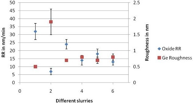
Integration of these novel materials on bulk Si is ongoing, and first CMP processes have been developed, but there is still a need to better understand and then optimize how the CMP processes work, IMEC notes. For example: removal rates should be tunable for Ge and SiO2, where the CMP process must stop; and polished Ge surface after CMP must be defect-free and with very low roughness (<0.5nm root mean square).
 |
| Oxide removal rate and Ge roughness for various slurries. The oxide removal rate and the Ge roughness are inversely proportional. Source: IMEC |
Thus the IMEC-CAMP collaboration aims to improve the understanding of these materials’ polishing mechanisms. Common understanding of Ge CMP is oxidation of Ge by a strong oxidizer, followed by abrasion of the oxidized Ge layer by abrasives in the slurry. Experiments on Ge disks and Ge-on-Si wafers examining the influence of different oxidizers at various pH values have already yielded a first finding, they report: the oxide removal rate and Ge roughness are inversely proportional, and further tests are planned to explore this correlation.
H2, inerts improve solid-phase epitaxy for Ge-on-Si
IMEC also is summarizing its recent work (published in Applied Physics Letters, in March 2009 and updated in Feb. 2010) in solid-phase epitaxy (SPE) of Ge-on-Si, noting how it can be "a valuable alternative" to conventional heteroepitaxial growth.
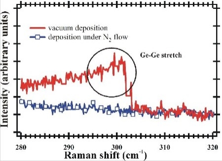
The presence of hydrogen at low temperatures, and/or inert species, they say, "significantly improves the quality of the Ge layers," which have resulting "excellent crystalline quality and low surface roughness" (0.4nm root mean square). In SPE, an amorphous layer is deposited on a crystalline substrate: e.g., using plasma-enhanced chemical vapor deposition (PECVD) with GeH4 or ultrahigh vacuum deposition (UHV). The presence of hydrogen, IMEC says, lowers the surface mobility of adsorbed Ge atoms, increasing the disorder of the deposited layer — which is beneficial to SPE where crystallization starts at the interface first. (Atomic hydrogen is also incorporated in the growing layer but does not affect crystallization, they note.) Similarly, fluxes of H2, N2, or other chemical inert species added during deposition by UHV also reduce surface mobility and thereby the structural ordering of the Ge layers.
Ge deposition is performed at low temperatures (typically 150°C), with crystallization done by thermal annealing (600°C in N2 atmosphere for 1min, though as low as 400°C can be applied). Annealing the structure initiates crystallization at the interface, continuing toward the surface — thus an epitaxial layer can be formed on the substrate. Conventional heteroepitaxial growth would require additional steps to reduce surface roughness, they note.
 |
|
Comparison of Raman measurements of Ge layers deposited in vacuum (red, |
April 26, 2010 – As with sister markets, demand for silicon wafers used in making semiconductors is expected to ramp up in 2010, driven by a single keyword: "innovation," according to analyst firm iSuppli.
 |
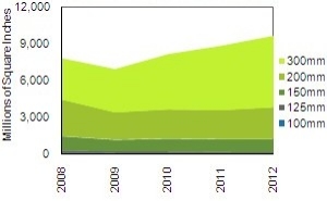
| Worldwide silicon demand by wafer size (MSI). Source: iSuppli |
Demand for silicon wafers shipped for semiconductor manufacturing is seen increasing 17% to 8.2 billion millions of sq. in. (MSI), rebounding from an -11% decline in MSI in 2009. For 300mm wafers, demand is expected to be well ahead of that pace: about 27% to 4.5B MSI. By contrast, 200mm wafer demand will grow just 7%, and just under 10% for 150mm wafers.
Looking ahead, the firm projects 300mm wafer demand will grow to 6.1B MSI, a 12.4% compound annual growth rate from 2008. Over the same period, 200mm wafers will have shrunk to 2.7B (a -2% CAGR).
Len Jelinek, iSuppli’s director and chief analyst for semiconductor manufacturing, summed up the rebound in wafer demand in one word: Innovation. "A major element in achieving innovation is the increasing adoption of 300mm wafers, which offer greater economies of scale and thus greater efficiency and lower cost than smaller wafer sizes," he explained.
Another factor: A typical period of recovery after a downturn, driven by technical/manufacturing achievements. After the 2001 recession, the chip industry embraced three major technical transitions: scaling to the 0.13μm node, incorporation of a new metallization scheme, and beginning of a transition to 300mm wafers.
And so it will be with the post-2008/2009 industry recession, iSuppli claims. This time, 300mm manufacturing has been fully embraced (>50% of all manufacturing), and 200mm will be phased out. This "aggressive transition" will put pressure silicon manufacturers, from companies who have yet to recoup their investments in 200mm tooling, the firm notes. (See iSuppli’s related report on this, "300mm wafers provide long-term cost reductions".)

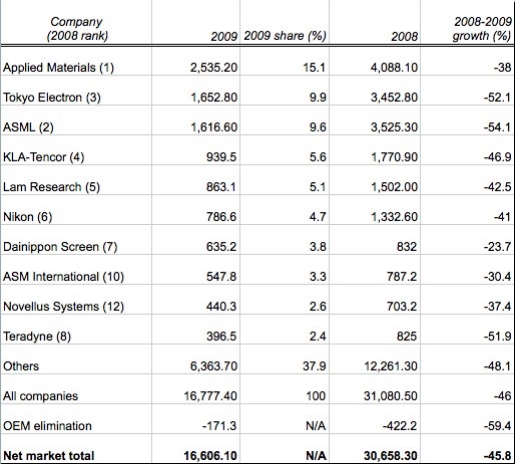
April 9, 2010 – Global semiconductor capital equipment spending totaled $16.78B in 2009, roughly a -46% dropoff from 2008 as chipmakers put the brakes on all but essential spending in order to preserve cash in response to the industry and global meltdowns.
Memory capex evaporated (-54%) as companies struggled with price erosion and profit losses incurred since the year before. Logic and mixed-signal spending was cut back too (-26%) mainly with only technology step-upgrades. But by year’s end, though, spending started to return — Gartner’s previous "final" tally for 2009 calculated added about $300M to its December projections.
Despite all the market turmoil, the top rankings of toolmakers stayed relatively intact, though some positions changed hands in what was essentially a battle of attrition. The top seven kept their positions, while Tokyo Electron retook the #2 spot from ASML; there were also a couple of shuffles at the bottom, Novellus pushing up the list and knocking Advantest out of the top 10 (they were 9th in 2008). AMAT actually increased its share in 2009 to 15.1% from 13.2%. Only three companies (AMAT, TEL, ASML) pulled in $1B in sales in 2009; last year there were six, and 10 in 2007.
 |
| Worldwide semiconductor manufacturing equipment vendors — revenue estimates in US $M. Data includes revenue from acquisitions in 2009 for the entire year; 2008 data is before acquisitions. Growth is organic as well as through acquisitions. (Source: Gartner) |
By process/tool type, wafer fab equipment (front-end) taking the brunt of it (-47%), as "the vast majority" of tool buys were for technology and not capacity, Gartner notes. But the backend sector wasn’t spared either (-40%). Packaging/assembly equipment (PAE) dropped 32%, though companies selling copper wire bonders "performed substantially better" than the rest of the sector. Gartner sees the PAE sector taking off as more companies clamor to take advantage of emerging advanced packaging technologies and markets, e.g., through-silicon vias (TSV).
Also gutpunched in 2009 was automated test, plunging 53% to $1.15B, though after an "essentially nonexistent" first quarter, business and visibility returned by year’s end. 2010 is setting up for "excellent growth" for the ATE sector across all major test equipment segments, particularly for memory test business which should more than double, says Gartner. (That environment might not last, though — just a month ago the firm established a notably less bullish outlook for ATE, citing likely consolidation among memory test firms and improved test techniques.)

