Category Archives: Materials and Equipment

April 15, 2010 – Researchers from Lawrence Berkeley National Labs say they have taken a big step forward in addressing one of the major challenges in graphene: figuring out an economical, high-quality and production-worthy way of making it.

Graphene’s unique properties are well known: excellent electron mobility (100× faster than silicon) and an atomic structure with great flexibility and mechanical strength. But manufacturability is a problem — current fabrication methods based on mechanical cleavage or ultrahigh vacuum annealing aren’t compatible with volume production, notes Yuegang Zhang, materials scientist at Berkeley Labs. "Before we can fully utilize the superior electronic properties of graphene in devices, we must first develop a method of forming uniform single-layer graphene films on nonconducting substrates on a large scale," he says.

In their work, published in Nano Letters, Zhang and colleagues used direct chemical vapor deposition (CVD) to synthesize single-layer films of graphene on a dielectric substrate (they evaluated single-crystal quartz, sapphire, fused silica, and silicon oxide). Hydrocarbon precursors were catalytically decomposed over thin copper films (100-450nm thickness) which were predeposited via e-beam evaporation on the dielectric substrate. Dewetting and evaporating the Cu films yielded single-layer graphene film on a bare dielectric. Scanning Raman mapping, spectroscopy, and SEM and AFM confirmed continuous single-layer graphene films coating metal-free areas of dielectric substrate, measuring "tens of square micrometers."

Click to Enlarge
Figure 1. To make a graphene thin film, Berkeley researchers (a) evaporated a thin layer of copper on a dielectric surface; (b) then used CVD to lay down a graphene film over the copper. (c) The copper dewets and evaporates leaving (d) the graphene film directly on the dielectric substrate.

"This is exciting news for electronic applications because chemical vapor deposition is a technique already widely used in the semiconductor industry," Zhang notes.

Improved control of the dewetting and evaporation could lead to direct deposition of patterned graphene for large-scale electronic device fabrication, and could be used to deposit other 2D materials such as boron nitride, according to Zhang. And although wrinkles in the graphene film following the dewetting shape of the copper introduce mobility-slowing strains, "if we can learn to control the formation of wrinkles in our films, we should be able to modulate the resulting strain and thereby tailor electronic properties," he said.

Moreover, observing the films after Cu evaporation will help the researchers learn more about growth of graphene on metal catalyst surfaces, which will help inform better control of the process, leading to ways to tailor the film properties or produce different morphologies, such as graphene nanoribbons, he added.

Click to Enlarge
Figure 2. (a) Optical image of a CVD graphene film on a copper layer showing the finger morphology of the metal; (b) Raman 2D band map of the graphene film between the copper fingers over the area marked by the red square on left. (image from Yuegang Zhang)


April 14, 2010 – Researchers from Berkeley Lab have developed a material dubbed "molecular paper," with properties that can be precisely tailored for applications such as chemical and biological detection.

2D "sheet-like" nanostructures are used in biological systems (e.g. membranes), with properties that have inspired further work in areas such as graphene. Ron Zuckermann and Ki Tae Nam with Berkeley Lab’s Molecular Foundry have created what they say is the largest-to-date 2D polymer crystal that spontaneously self-assembles in water, combining the structural complexity of biological systems with a durable architecture needed for membranes, or for integration into functional devices. The sheets — 2-molecules thick and hundreds of sq. molecules in area — are made of peptoids that can flex and fold like proteins.

Unlike a typical polymer, each "building block" of the nanosheet has what the researchers call "structural marching orders," suggesting its properties can be tailored to be application-specific — e.g., to control the flow of molecules, or serve as the platform for chemical and biological detection. The building blocks for peptoid polymers are also "cheap, readily available," and generate high yields, another advantage over other synthesis techniques.

"Our findings bridge the gap between natural biopolymers and their synthetic counterparts, which is a fundamental problem in nanoscience," stated Ronald Zuckermann, director of the biological nanostructures facility at Berkeley Labs’ Molecular Foundry. "We can now translate fundamental sequence information from proteins to a non-natural polymer, which results in a robust synthetic nanomaterial with an atomically-defined structure."

"The scientific possibilities that come with this achievement challenge our imagination, and will also help move electron microscopy toward direct imaging of soft materials," added paper coauthor Christian Kisielowski from the National Center for Electron Microscopy (NCEM). The group also achieved another landmark by observing individual polymer chains within the peptoid material, confirming the chains’ ordering into sheets and stability during imaging.

Their work has been published in Nature Materials.

by Michael A. Fury, Techcet Group

April 14, 2010 – The second day (Tues. 4/6) of the MRS Spring 2010 meeting in San Francisco ramped up to full throttle, with 38 symposia running in parallel. Highlights included CVD for Cu interconnects, controlling low-k etch-stop layers, inkjet-printed memory, materials challenges for future FETs, and "atom hopping" in graphene.

(See also: MRS Day 1 discussions, including charge-trapping NVM, organic electronics, graphene, and solar photovoltaics.)

(Underscored codes at the beginning of papers reviewed refer to the symposium, session and paper number; additional presentation details can be found in the MRS Spring 2010 program.)Click to Enlarge

F3.4. Yeung Au from Harvard described a selective chemical vapor deposition (CVD) Mn process for self-aligned adhesion and barrier layers in Cu interconnects. The Mn diffuses rapidly into the Cu, but after the capping layer is deposited, it diffuses back to the Cu surfaces due to the strong thermodynamic drive to form Mn nitride, oxide, or silicate. As a result, the Mn does not degrade the Cu conductivity. The dielectric surfaces can be passivated against Mn deposition, resulting in a selectivity of ~1100:1. The Mn also diffuses to the Cu sidewalls and trench bottoms, forming a ‘zero thickness’ diffusion barrier, thus allowing Cu interconnects without the requisite Ta/TaN or RuO2 barrier layer.

F3.5. Hung-En Tu of Taiwan’s National Chiao-Tung University explored the use of functional groups in porogen precursors to control the pore size and porosity in low-k SiCxNy etch-stop layers while maintaining the mechanical strength of the films. Polystyrene (PS) and epoxycyclohexane (ECH) were evaluated as sacrificial porogens. As PS concentration increased, both % porosity and pore size increased (from 18nm to 35nm). As ECH concentration increased, only % porosity increased; pore size was constant at 21nm.

G4.2. Tse Nga Ng from PARC showed a novel inkjet-printed NV FeFET memory device that uses silver electrodes and can retain 50% of output current over seven days. The experimental design allowed good separation of the various contributions to performance degradation, thus providing a good learning vehicle for further development.

J1.4. DARPA’s Todd Hylton discussed "Electronics for Intelligent Systems: Concepts and Devices." An intelligent system is defined as a universal computer capable of executing any input-output operation. A related concept, the thermodynamic state machine, responds to environmental input and evolves its internal algorithms to achieve a stable state relative to its environment. These behaviors can be exhibited by a TiO2/α-Si memristor device, which makes them suitable for casting in the role of synapses between transistors acting as neurons. The underlying objective is to build a machine that can evolve by its own actions, and not have all of its structure pre-embedded by the designers.

J1.5. Sayeef Salahuddin from UC Berkeley spoke on the possibility of negative capacitance in ferroelectric materials. Such behavior would significantly reduce the power dissipation in transistors. As a point of reference, the annual power consumption of all of the world’s Internet data centers is 150BkWh, and would rank between the national power consumptions of Mexico and Iran. The principle depends on the natural metastable state of the ferroelectric. While there is still no conclusive experimental evidence for -C, these effects are thought to be showing up in ferroelectric gate devices, starting with work presented at the 2008 IEDM.

J2.2. The grand materials challenge of reinventing the FET transistor was presented by Tom Theis of IBM Research. The convergence of device shrinks and fundamental limits puts us in the position of introducing new materials at the same time we are tinkering with the fundamental device physics. Historically, device scaling had been based on maintaining a constant field. Recently, we have switched to constant voltage scaling to ensure that we can turn the devices on and off. Some things to expect in our future include: CNT tunnel FET designs; a gate ferroelectric sandwiched between two paraelectric films; spin FET, though polarization needs to improve by several orders of magnitude.

J2.3. Tao He of the Beijing National Center for Nanoscience and Technology talked about controllable molecular modulation of conductivity in Si devices. As devices scale below 32nm, some structures may be controlled by as few as ten dopant atoms. Grafting molecular monolayers between the source and drain is one method for stabilizing conductivity. Such grafted layers can confer both gating and doping effects. These molecular effects have been seen to manifest through a 4.92μm thick Si layer.

J2.4. Sumit Chaudhary of Iowa State extended his group’s interest in OPV to develop a TiO2 ultrathin-film memristor by electrochemical anodization. Such devices are more commonly fabricated by ALD or sputtering. This work is expected to result in a workable design for a two-terminal memristive device.

J2.5. Robert Westervelt of Harvard CNS gave a prospective of graphene for future electronics. Electron movement in graphene is ballistic, with velocities of c/300 (where c is the speed of light). Devices can be contemplated in 2D (sheets), 1D (ribbons) or 0D (flakes). The flakes can hypothetically perform spintronic logic. A TEM beam can be used to cut graphene sheets for atomic-scale devices. The carbon atoms at the cut edge were observed in real time to hop around to find the lowest local energy state using a Zeiss Libra 200 TEM, which has a resolution of ~0.10nm — true atomic resolution. The video of atom hopping gets my vote for one of the coolest things presented all week.

J2.6. Jeremy Levy from the U. of Pittsburgh promised oxide nanoelectronics on demand, describing a method for producing extreme nanoscale electronic confinement at the interface between two normally insulating oxides, LaAlO3 and SrTiO3. A high-mobility electron gas forms at the interface. Using a conducting atomic-force-microscope probe, he can create nanoscale conducting islands, wires, tunnel junctions, diodes, transistors and photoreceivers with spatial dimensions comparable to the diameter of a single-wall carbon nanotube (~2nm). These structures are created in ambient conditions at room temperature, and can be erased and rewritten repeatedly.

Q1.1. John Rogers of the U. Illinois at Urbana has expanded from silicon to compound semiconductors for flexible, stretchable electronics. Using a simple wet etch undercut method, he fabricates triangular wires 0.5-1.0μm on a side out of semiconductor grade Si, GaAs, AlInGaP, and InP. Fully functional GaAs RF circuits were separated as a 200nm thick membrane from the bulk wafer and transferred to a plastic substrate, where they were integrated with stretchable interconnects. The resulting device continues to exhibit GHz response. This technology has been used to fabricate flexible sensor membranes that can be used in direct contact with a medical patient’s heart or brain tissue.

Q1.3. Lei Liao at UCLA fabricated nanoribbons and nanowires of high-k Al2O3 for use as the gate dielectric on top-gated graphene transistors. This high-mobility configuration gives a transconductance that is 10× higher than previous back-gated devices.

Q1.4. Michael Wang at Simon Fraser U. has developed a method for electric field-directed self-assembly of flexible semiconducting Se nanowires. The wires are precipitated from a solution of H2SeO3 and hydrazine, which is always fun in the lab. Rapid evaporation of the octanol solvent produces a non-woven fiber mat. Se is photoconductive, which lends itself to a variety of optical devices and switches.

Q1.5. David Taggart of UC Irvine characterized the electrical and structural properties of PEDOT nanowires produced by lithographically patterned electrodeposition. The conductivity of the resulting material is up to 4× better than thin-film PEDOT. In addition, the Seebeck coefficient of the nanowires is 2× better than bulk PEDOT for thermoelectric devices.


Michael A. Fury, Ph.D, is senior technology analyst at Techcet Group, LLC, P.O. Box 29, Del Mar, CA 92014; e-mail [email protected].

by David Hwang and Jurron Bradley, Lux Research

April 1, 2010 – Since pioneers Showa Denko and Hyperion Catalysis first started producing multi-walled carbon nanotubes (MWNTs) in 1983, dozens of companies have entered the fray, looking to claim a share of a potentially massive market. However, market adoption has taken much longer than many expected, ultimately driving companies without proper financial backing into the red. Despite the gloom, MWNT suppliers aren’t an endangered species, as more than 35 commercial suppliers are still active.

Across the industry, producers are increasing capacity with hopes of lower costs and greater market adoption. The ongoing game of one-upsmanship is pushing market leaders to increase their capacities by more than four-fold in order to prevent becoming priced out of the market by their competitors. In 2008, global MWNT production capacity totaled just 423 tons, but today it weighs-in at 1,334 tons, a whopping 215% increase. Moreover, once current capacity expansions are completed (likely in 2010 and 2011), total capacity will swell to 2,389, a 416% increase over 2008 levels. Note that some plans to scale-up are confidential and thus are not included in the table below.

Click to Enlarge
Figure 1. Key MWNT suppliers. (CCVD = catalytic chemical vapor deposition; SME = small or medium-sized enterprise)

Looking closer, production capacity is owned disproportionately by the largest five suppliers: Showa Denko, CNano Technology, Arkema, Nanocyl, and Bayer MaterialScience. CNano Technology completed construction of its 500 ton production facility in June 2009, and Showa Denko finished building a 400-ton plant in March 2010, bringing its total up to 500 tons as well, making them the two largest suppliers. The other three suppliers — Arkema, Nanocyl, and Bayer MaterialScience — are scheduled to bring multi-hundred-ton facilities online in late 2010 and early 2011. Together, the five largest suppliers operated 54% of the world’s total production capacity in 2008 — and after completing the planned scale-ups, they will operate over 86% of the global production capacity in 2011. The massive scale-up and resulting cost reduction will further cement their dominance over second- and third-tier suppliers, making it even harder for the smaller producers to compete.

Click to Enlarge
Figure 2. Announced MWNT production capacity.

Don’t fall for the hype, however — because the market isn’t expanding at the same rapid scale-up rate. In fact, with a few exceptions, average utilization of production capacity per company is likely in the low double-digit percent. Specifically, we estimate that producers sold only 124 tons of MWNT in 2008, meaning a 30% utilization of capacity globally. With the producers undergoing such massive scale-ups, the amount of idle capacity is set to expand even further in the near-term, as sales grew approximately 35% in 2009, but production capacity more than doubled. This oversupply situation will likely persist at least through 2015.

While the extra capacity will not equate to additional revenue immediately, it will help MWNT’s long-term prospects. For one, scale-up to date has driven prices down from the dollars/gram range to $100/kg today, and producers ultimately hope to achieve $50/kg. When MWNTs were dollars/gram, industries turned their backs — but now that the economics for using MWNTs are quickly becoming favorable (especially in composite applications) they’re showing a renewed sense of interest. Additionally, further price reductions will help MWNTs expand out of small-volume niche applications like fishing poles and into larger and more cost-sensitive markets like car body panels. More broadly, producers are pushing their products into the automotive, aerospace, electronics, wind power, and energy storage industries — all of which will to drive demand for the next decade.

Biographies

David Hwang received a BSE in Bioengineering from the University of Pennsylvania and is research associate at Lux Research Inc., e-mail [email protected].

Jurron Bradley received his Ph.D in chemical engineering from the Georgia Institute of Technology and is senior analyst at Lux Research Inc.

March 29, 2010 – Mapping much of the semiconductor equipment sector along two sets of data reveals that there might be conditions brewing that could create "the catalyst, finally, for consolidation in the equipment space," according to Barclays analyst CJ Muse.

To be sure there have been a number of M&A moves in the past year or so: Applied Materials/Semitool, Asyst/Peer Group/Crossing Automation, Semilab/SDI, FormFactor/Electroglas, Oerlikon-ESEC/BE Semiconductor, and in recent days Jordan Valley/Metrosol and Tegal/OEM Group, just to name a few.

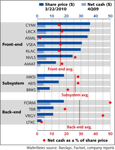
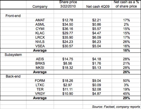
Industry winds seem to be building, as demand continues to be heavy and is expected to stay brisk probably through year’s end and into 2011. And companies are starting to build up cash again as cost-cutting efforts are realized, tool shipments improve, and profit needles swing back to black. From an investment perspective, Muse postulates that cash-flow generation as a percentage of share prices reveals that many companies in the semiconductor equipment space have done a very good job of revitalizing their business models at given revenue levels than in previous cycles, particularly among backend and subsystems suppliers. The average cash/share price is now 29%, and could rise across the board by 500 basis points in 2010 (e.g., 16% to 21% for front-end process equipment firms), and another 700-1100 basis points exiting 2011, Muse notes. And companies aren’t getting enough credit for their operational improvements, he notes, as industry watchers celebrate order momentum instead.

Click to Enlarge


The result? With ~80% capex growth predicted for 2010 and another 15%-20% expected in 2011, sales and cash generation should rise accordingly, assuming no new buyback programs and substantially increased cost structures. And thus, valuations should start glowing both from price/earnings as well as "enterprise value"/normalized sales. Many firms are currently trading at ≤1.0x levels, he points out — and given that normalized sales are based on mid-cycle (not peak) wafer-fab equipment (WFE) levels, such multiples are "highly attractive," Muse points out.

Click to Enlarge

The upshot of Muse’s research: Investors should take a more serious consideration of order strength and valuation and rally the sector stocks. If they don’t, and these ratios continue to become more and more attractive, "look for this to be the catalyst, finally, for consolidation in the equipment space," he writes.

March 24, 2010 – Showa Denko KK (SDK) has completed a new 400 tons/year plant for its new carbon nanotubeswhat it claims is currently the world’s largest CNT factory — with commercial production slated to begin next month after a trial run.

The site will supply SDK’s new VGCF-X products, CNTs with very high electrical conductivity and dispersibility optimized for resin composite applications, the company says. Initial use will be in static-free plastic cases for electronic devices, including semiconductors and hard-disk media. The company also anticipates use in applications requiring CNT’s added strength, such as transport machinery parts.

SDK’s VGCF technology was first developed in 1982, with a 20 tons/year commercial CNT plant ramped up in 1996 in Kawasaki; capacity was expanded to 100 tons/year in 2007. A composite-grade version of VGFC-S was developed in 2008 targeting composite rubber for oil exploration/drilling applications.

March 19, 2010 – The chip industry keeps chugging along the recovery road, with another "dramatic" month compared to the depths of where we were a year ago, according to the latest monthly figures from SEMI.

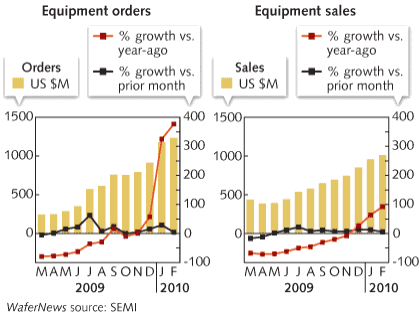
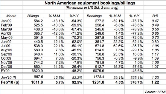
According to North American-based manufacturers of semiconductor equipment, demand rose about 4%-6% sequentially in February, with bookings rising to about $1.23B, and billings crossing the $1B mark to $1.01B. (Both figures are a three-month average). Comparisons to the same period a year ago look stellar, since that was the low-water mark of the downturn: Feb. 2010 bookings were up 377% Y/Y, and billings up 92.5%. With the continued demand, the book-to-bill ratio (B:B) stayed well above parity at 1.23 — meaning $123 worth of orders were received for every $100 shipped during the month.

Click to Enlarge

Some more impressive comparative statistics:

  • Bookings are at their highest in two and a half years (Sept. 2007, $1.235B). January had been highest in nearly two years.  For a second straight month, final bookings tallies for the previous month had to be revised upwards by about $50M.
  • Billings are at their highest in a year and a half (August 2008, $1.06B), the last time they crossed the $1B/month mark, and have been rising sequentially for 10 consecutive quarters.
  • Perhaps the most impressive statistic: Jan-Feb represent the first sequential >1.2 B:B months in more than seven years (Jun-Jul 2002, 1.26-1.22). The B:B also has been above parity for eight straight months. For a statistic generally viewed as the key measuring stick for business coming in (orders) vs. going out (sales), that’s an important number to watch.


Click to Enlarge

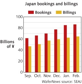
The numbers continue to look very good in Japan’s semiconductor equipment sector as well. Orders for chip tools crept up 1.5% to about ¥86.3B, while sales rose 3.4% to ¥64.6B, according to the Semiconductor Equipment Association of Japan (SEAJ). (Like the SEMI numbers, year/year comparisons are strikingly good: orders up 531% and sales up 66% vs. Feb. 2009.) Though the month-on-month growth is a bit slower than in recent months, Japan’s B:B remains at very high levels above 1.34 — it has dipped below 1.30 only once in the past seven months.

Click to Enlarge


March 19, 2010 – No surprise that 2H09 was a comeback period for semiconductor equipment and materials suppliers, but new "final" numbers from SEMI suggest some late-season changes in behavior in some regions, and ultimately sets the stage for a better 2010.

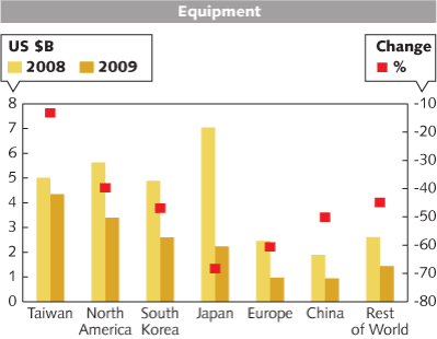
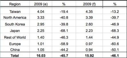
Overall, 2009 equipment sales came in about where SEMI thought they would in its Nov. 2009 estimates: around $16B, a -46% dropoff vs. 2008. At a regional level, spending rates declined by double-digits for everyone. Tops in spending was Taiwan with $4.35B, followed by North America ($3.39B), Korea ($2.6B), Japan ($2.23B), Rest-of-World with $1.44B (covering Singapore, Malaysia, Philippines, Southeast Asia, and smaller global markets), Europe ($970M), and China ($940M).

Stronger-than-expected 4Q09 spending seems to have helped Taiwan put on an extra $300M compared with the initial forecasts, ending the year at a -13.2% decline instead of nearly -20% as had been anticipated. "TSMC and the packaging houses boosted their capex plans several times throughout 2009 once the market recovered off the bottom," Dan Tracy, SEMI’s research development director for industry research and statistics, told SST. Other regions came up a bit short — China was about $150M short, resulting in -50% vs. -44%; while Korea came in about $350M shy, resulting in a -47% Y/Y decline vs. 40%.

Click to Enlarge
Click to Enlarge 
Semiconductor equipment sales in 2009 by region: estimated (Dec.2009) vs. final (Mar.2010). Note that totals may not add due to rounding. (Source: SEMI/SEAJ)

By equipment type, SEMI’s final numbers are in close agreement with what it predicted in early December: a -46% decline in wafer processing equipment (to just under $12B), -31% for assembly/packaging equipment (to about $1.4B), and -55% in test equipment (to $1.55B); "other" frontend equipment declined about -44% to about $1.12B.

Tracy told SST that the final 2009 numbers haven’t yet been plugged into SEMI’s full equipment forecast for 2010 and beyond — but the group’s initial outlook for 2010 fab spending was recently bumped up to a nearly 90% increase (to $30.9B) instead of prior 66% outlook, thanks to increased capex plans mainly by foundries and memory companies, for both postponed and new projects. Installed capacity is now expected to grow 5%-6% to ~16.1M wafers/months.

The final numbers were compiled from data submitted by members of SEMI and the Semiconductor Equipment Association of Japan (SEAJ), across seven major semiconductor producing regions and over 22 product categories: e.g., wafer processing, assembly and packaging, test, and other front-end equipment (such as mask/reticle manufacturing, wafer manufacturing, and fab/facilities equipment).

Materials gains ground in 2H09 too

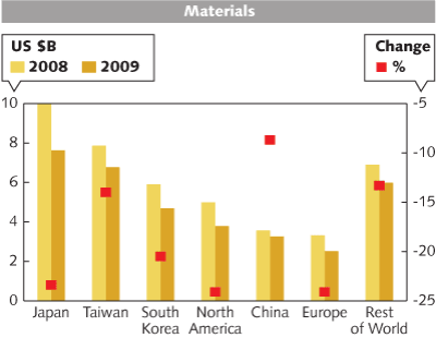
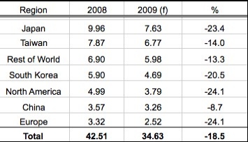
Semiconductor materials contracted by -19% in 2009 to $34.6B as the industry "reacted quickly" to the downturn early in the year; in the end, the downturn for materials sales wasn’t as bad as the 2001 crash (-26%). Sales were split almost evenly between wafer fabrication materials ($17.9B) and packaging materials ($16.8B); in 2008 the gap was wider ($24.2B and $18.B, respectively). The bigger slide in wafer fab materials was attributed to big decreases in silicon revenues, SEMI notes.

By region, Japan remains the largest consumer of semiconductor materials (22%) due to its large base of wafer fab and advanced packaging users; almost every region saw declines by double-digits (China was -9%), though increases in gold metal prices helped offset declines in those regions with strong packaging bases, SEMI notes.


Click to Enlarge
Click to Enlarge
Semiconductor materials sales by world region, in US $B.
Note that totals may not add due to rounding. (Source: SEMI)

by Roger Peirce and Brad Williford, Simco

Executive overview
In semiconductor manufacturing, the die attach operation takes the singulated chips from the wafer and places them in a new target location (such as a tray, substrate, printed circuit board, etc.). Four general categories of electrostatic discharge (ESD) failure modes have been observed at this operation, namely: charged device model (CDM), field induced model (FIM), machine model (MM), and charged board model (CBM). We have identified seven distinct mechanisms in typical die attach operations that can and do cause ESD damage to the chips being handled. They are reviewed here.

March 17, 2010 – First, to hold semiconductor wafers in place and to facilitate subsequent operations at wafer sawing, back grinding, scribing and breaking, wafer probing, die attach, and various pick and place operations, typical semiconductor procedures include the mounting of wafers on a sheet of adhesive tape material (blue tape is common) that is held in place by an outer metal ring assembly. As the adhesive tapes are insulative, they become highly charged whenever contact is made with the material. Charges of 20kV and higher are typical from even just slight contact and separation (rubbing). This charging of the adhesive tape material, in turn, causes the wafer to become charged inductively. The devices on the wafer can be subsequently damaged when discharged by any large conductor such as operators, metal fixtures, robot arms, stages and chucks, etc.

The die-attach/chip-picking operations where the diced, individual chips are removed from the adhesive tape assemblies have been especially interesting from a device failure viewpoint. We have found this particular operation has resulted in perhaps more documented CDM ESD damage than any other single operation in typical semiconductor manufacturing processes. That statement is based on literally scores of case studies where this operation was analyzed, leading to documented yield improvements. And there is more to understanding the associated failure modes here than meets the eye. It has been determined that at least seven different failure mechanisms to chips can exist here as we will describe in detail.

Charging of tape from operator handling. Operators, or other types of handling mechanisms, cause the adhesive tape material to become charged (Figure 1a). The devices on the tape now diced from the wafer charge inductively and then become discharged either by operators (with tweezers typically) or the conductive collet on the automatic chip-picking equipment, thereby causing CDM damage to the device.

   
Figure 1. Tape charging/recharging mechanisms from a) operator handling, and b) chip picking, respectively.

Recharging of tape from chip picking. Even if the charge on the tape is removed before the operation begins, another chip charging mechanism subsequently occurs. As each chip is lifted off the tape, a resulting charge remains on the tape in that "missing chip" area (Figure 1b). As the chip removal operation advances, this "missing chip" area (exposed tape) increases and the field strength becomes more dangerous. The remaining chips become charged by induction from this field — and can be subsequently discharged. Typically, the discharge occurs through the conductive collet on the equipment. In our past case studies, the chips damaged from this mechanism tend to be located near the end of the picking process — as might be expected since the field strength becomes stronger and stronger as more and more chips are removed. Even if charge is removed on the tape assembly before the operation begins, the tape will recharge during the chip picking process.

Charging of chips during separation from tape. An ionizer is typically employed to remove the charging mechanisms detailed above. A third charging mechanism exists during this operation — one that cannot be eliminated strictly by employing an ionizer above the chip picking collet. The next failure mode to be described has resulted in many cases of device damage and it is not very well understood or addressed typically. (It is emphasized here that many process engineers now implement ionizers above the chip-picking collet so that ESD risks from the high charge generating nature of these tape assemblies are eliminated. However, the overhead ionizer cannot — and does not – eliminate this next risk.) As the chip is lifted off the tape, friction and separation can cause the chip to charge dramatically. We have measured (via Faraday cup measurements) chip charging in excess of 10kV from this event. This chip charging is especially dangerous as the conductive collet is already in contact with the chip and can cause an immediate discharge. This failure mode occurs so rapidly (nsec to μsec range) that standard ionizing techniques typically are not able to prevent the damage. We have been successful using the approach of changing the collet material to a less conductive material and implementing custom ionization. The custom ionization should be implemented so that the chip is discharged on its way from the separation point to its next conductive contact which is most likely a conductive container, a printed circuit board assembly, a substrate, etc., that can potentially discharge it. That distance can be short, and the operation can be rapid — so intelligent, custom, selection of the ionization device is essential in this case.

Pogo pin discharge. Some die attach/chip-picking machines also include an additional "pogo pin" mechanism (that can be conductive) underneath the tape assembly. It is designed to push up the chip slightly so that the overhead collet has an easier time lifting the chip off the sticky tape surface. We have also verified chip damage that was traced to the discharging of the charged chip via this pogo pin, although this failure mode has been observed less in our case studies. The signature damage earmark on these failures (SEM images, etc.) is dramatically different than the signature damage typical in failure mode #3 above, as might be expected from a top versus bottom discharge. It is important to note that there have been documented cases where discharges still occurred to the pogo pin with wafers/chips that had insulative bottom layers.

Picked chip discharging into target location. Once a chip has been picked (lifted off of the tape surface by the collet) on this type of equipment, it subsequently is transported via the moving collet to a target location on the machine such as a printed circuit board assembly, or a substrate, or a conductive container, tray, or waffle pack, etc. If the chip is still charged from any one of the mechanisms reviewed above, it can be damaged by a discharge at its target location (Figure 2). It is very important to insure that no charge remains on the chip before it is placed into its final resting place on the machine.

 
Figure 2. A chip being "picked" off the tape surface by a collet.

Charged target location. Yet another failure mode can exist with this type of equipment. Even if all of CDM risks addressed in modes 1-5 above are addressed and eliminated, a machine model (MM) risk can be present if the target location has become charged (Figure 3). We have observed cases for example, where the chips were placed onto charged bare printed circuit boards (PCBs). The PCBs were initially charged from the processing operations leading up to their contact with the chip. Printed circuit wiring can discharge into the chip in this case; such a condition is a "mini" machine model failure mode.

 
Figure 3. Printed circuit wiring can discharge into the chip.

Chips recharging in target locations. And finally, it is possible for the chips to become recharged and subsequently discharged before the final assembly leaves the die attach machine. The two most common causes of chip charging at this late stage are typically the result of existing charge on the printed circuit board plastic that inductively couples into the chips on the board and triboelectric charging of the entire assembly from sliding on a conveyer belt or other surface (CBM failure mode) (Figure 4).

 
Figure 4. The entire final assembly can charge and discharge.

It is important to verify that none of the above failure modes exist in this operation. We have verified (confirmed) yield losses on occasion from each of these seven failure modes.

Conclusion

Substantial amounts of charged device model ESD damage are not only possible, but are probable in semiconductor die attach operations if the necessary ESD controls are not in place. Yield losses due to CDM and MM electrical damage due to these operations can be substantial [1]. Eliminating the potential risks is critical for state-of-the-art reliability and profitable operations.

Biographies

Roger J. Peirce received his BSEE from Fairleigh Dickinson U. and is director of technical services for Simco Ionization for Electronics Manufacture, an ITW Company, 2257 North Penn Rd. Hatfield, PA. 19440; ph.: 215-997-3430; e-mail [email protected].
Brad Williford received a BSME in mechanical engineering and an MBA from Virginia Tech and is global semiconductor OEM accounts manager for semiconductor ionization products at Simco Ionization for Electronics Manufacture, an ITW Company. 2257 North Penn Rd. Hatfield, PA 19440. Mr. Williford has a bachelor’s degree in mechanical engineering (B.S.M.E) and master’s degree in business administration (MBA) from Virginia Tech. PH. 919-567-0145, e-mail [email protected].

References

[1]. R.J. Peirce, "Improved yield through comprehensive CDM ESD failure analysis," Solid State Technology, pp. 32-40, May 2007.

(March 15, 2010) MORRIS TOWNSHIP, NJ — Honeywell (NYSE: HON) Electronic Materials debuted a printable thermal management material designed to help manage the high heat produced by increasingly powerful semiconductors in portable computing devices such as laptops and netbooks.

Honeywell PCM45M-SP builds on Honeywell’s Electronic Materials’ existing line of thermal management materials. As semiconductors become more powerful and smaller, more heat is being generated in the confined spaces where semiconductors are packaged for end-use applications. This tremendous heat can damage the semiconductor or degrade its performance, and it can damage the device as well.

“Mobile computing devices such as laptops and netbooks are placing increased demands on thermal management materials to enable high performance and ensure a long lifespan,” said Tim Chen, packaging leader for Honeywell Electronic Materials. The product combines phase-change chemistry in an innovative formulation specifically designed for these types of mobile devices.

In typical mobile computing applications, chip temperature rises steeply at start-up and remains high during operations. PCM45M-SP is designed to meet these specific thermal management requirements, delivering reliable power cycling performance where other thermal materials would typically fail.

PCM45M-SP can withstand more than 1,000 hours at 150