Category Archives: Semicon West

by Michael A. Fury, Techcet Group

Click to Enlarge July 20, 2010 – The third & final day of SEMICON West 2010 was quite a bit more relaxed with everyone crashing following their sugar highs at the NY Loves NanoTech dessert event the night before. Folks seemed more willing to just sit down and talk for a spell.

Mike Ciesinski, president & CEO of the FlexTech Alliance (which now resides in SEMI HQ) gave me an update on the next quarterly workshop on flexible & printed electronics: Advanced Materials and Processes Enabling Thin Film PV R2R Nanomanufacturing, coming up Sep. 15-16 in New Bedford, MA.

Robert Rossi (VP) and John Welty (polishing manager) at Spartan Felt gave me a fascinating tour through the world of polishing pad applications and pad types beyond the domain of semiconductor CMP. It really is a humbling experience to see how much technology goes on outside of our semiconductor-centric world.

SEE ALSO:
Day 2: Shoes vs. phones, CMP users, updating Art’s Law
Day 1: CMP, slurries, metrology, thermal, zombies, observations

In my Day 2 blog, I promised some follow-up to some questions raised at the CMPUG Q&A. Some additional data and presentations can be found on the Confluense LLC Web site, and it is instructive to watch their video posted on YouTube. For anything else, I recommend contacting Confluense directly. The other subject that came up was the button pad from SemiQuest, which has posted some early data on its Web site — but the most recent information, including a description of the pad itself, is posted online with the May 2009 NCCAVS CMPUG proceedings, in a presentation called "Opportunities and Challenges in Developing a Low Defectivity Pad Platform".

It’s always fun to see things come full circle. Bob Roberts, who sold me my first (not the first) CMP polisher at IBM East Fishkill in ~1986, is now back in San Luis Obispo, CA as Strasbaugh‘s executive director of advanced technologies, after several years on the East Coast. He and the Strasbaugh team launched their new STB P300 CMP system at the show, targeting small-lot, high-mix manufacturing environments.

I wasn’t able to spend much time at the Intersolar events over at Moscone West this year, but I did get a personal tour of the eIQ Energy system for connecting solar panels in parallel instead of series, from QA manager Bob Sherrill. It’s instructive to watch their video on YouTube — apparently it’s a pretty big deal to be able to connect panels in parallel for overall system efficiency. It has the added benefit of being able to use panels from different vendors, even different technologies, in a single integrated system. One of their local demo sites is the Big O Tire shop in Dublin, CA.

One thing I noticed about the Intersolar show is that folks were walking around with beers at 1pm, which I choose to believe is an indication of just how well things are going for the solar power industry. Had I seen this in the semiconductor show, I would have had a completely different interpretation for the early afternoon drinking, a much sadder one.


Michael A. Fury, Ph.D, is senior technology analyst at Techcet Group, LLC, P.O. Box 29, Del Mar, CA 92014; e-mail [email protected].

by Michael A. Fury, Techcet Group

July 19, 2010 – The second day of SEMICON West 2010 started earlier than usual for over a hundred folks with the now-traditional ElectroIQ (PennWell Publishing) Marketing & Technology Update Breakfast. Among the tidbits gleaned from Bill McClean of IC Insights:

  • WalMart’s annual sales of $400B are larger than the entire semiconductor capital equipment market.
  • Following each of the five economic downturns and recoveries over the past 30 years, the semiconductor industry has experienced double-digit growth, so we can expect that again now.
  • The next semiconductor downturn can be expected in 2013.
  • Only 15 companies hold 92% of the global capacity for 300mm leading edge chip manufacturing.

Click to EnlargeAt the same breakfast conclave, Proteus Biomedical CEO Andrew Thomas wove an interesting tale that took us to some unexpected places. Of the 7 billion people on the planet, only 3.5B wear shoes — yet 4.5B own a cell phone, even though many of them earn <$10/day. Clearly, electronic devices have tremendous market penetration power. Many of those cell phone owners never have and never will see a doctor in their lifetimes. Andrew aspires to reach those people with medical attention by driving the healthcare business model — which is driven today by the richest 10% in the world — toward the electronics business model, which is doing a far better job reaching the poorest among us. One of the elements of his system is a digestible electronic pill that delivers the medicine and reports conditions from the inside of the body before it dissolves away. Think of it as OnStar for your body. I am reasonably (but not 100%) certain that these devices were not part of the breakfast.

About 50 people attended the SEMI Chemical & Gas Manufacturers Group (CGMG) meeting in the Marriott. Among the highlights from Jim Hannah (IBM), Roger Gosset (Freescale), and Lita Shon-Roy (Techcet):

  • Growing concern about China restricting access to rare earth metals important to semiconductor production.
  • Less toxic alternatives to TMAH are needed.
  • More formulated cleaning chemistries are needed, with better selectivity targeting; a larger process window is becoming a more important differentiator.
  • Reduction of trace metals in lithography materials to 1-5 ppb.
  • Greater sensitivity to ‘blood minerals,’ analogous to ‘blood diamonds.’
  • Ta, Ti, and anhydrous HCl are examples of movement in global supply chain issues impacting supply reliability for semiconductors. We like to think we are a huge, important industry, but we are a drop in the bucket for many materials.
  • The drive to reduce industry solvent usage is focusing on reducing the volume per wafer, not looking for dry (plasma or scCO2) cleaning alternatives.
  • The need for new materials continues to be severely challenged by the misalignment between huge fixed R&D costs for product development and qualification, vs. very tiny total available markets.

A number of companies were present at the show without having a booth on the floor. SAFC rented out a restaurant above the entrance to the North Hall and had a wonderful venue for lunch and cocktail receptions and all the happy customer meetings one could hope for.

SEE ALSO:
Day 1: CMP, slurries, metrology, thermal, zombies, observations

The NCCAVS CMPUG meeting was held in a presentation area in the South Hall. While these meetings in past years have been good networking opportunities for CMP folks, as well as a quiet respite from the buzz of the show floor in a closed meeting room, this floor venue proved to be an exercise in patience and stamina. It’s tough enough to concentrate with the constant hall noise, but the periodic interruptions by the SEMI announcer are impossible to compete with. To make matters worse, the number of standees was about 2× the number of folks who were lucky enough to find a seat. I really do hope we return to the separate room in coming years.

Presentations from the CMPUG session (and all of the other NCCAVS sessions) will be posted as usual on the NCCAVS Web site in the coming weeks. Some highlights from Robert Castellano (Information Network), Karey Holland and myself (Techcet) and Mike Corbett (Linx Consulting):

  • The transition from 200mm to 300mm cost $25B and took 11 years; expect about the same for the transition to 450mm.
  • Europe is supporting 450mm in the hopes of establishing a competitive niche.
  • A 15%-20% ROI for 450mm tool development would require the construction of 4-8 450mm fabs/year for the next 15 years — and this doesn’t seem likely.
  • A SEMI working group has reported little upside benefit and high downside risk for 450mm.
  • The CMP pad and slurry markets are recovering quickly from the recession, and are likely to exceed the 2007 peak by next year if not later this year.
  • Asahi Glass is enjoying a rapid expansion of their market share for CeO2 STI slurry.
  • Some lasting effects of the latest recession include accepting lower purity sputter targets, using HfCl4 instead of more expensive Hf organometallic precursors, increasing the level of POU slurry dilution, and using more home-brew PCMP formulations rather than commercial products.
  • From now thru 2014, expect an 11% CAGR in the number of CMP wafer passes in fabs globally.
  • By 2014, ~10% of all CMP wafer passes will be for 22nm technology.
  • NexPlanar is expected to be among the last VC-funded CMP startups.

I also had some Q&A regarding SemiQuest button pads and the Confluense Pad Surface Manager, which I will address in tomorrow’s blog.

SEMATECH hosted a nice reception Weds. evening in the Marriott. This gave me a chance to visit at length with Lloyd Young, fab manager at East Fishkill Building 322 through several company reincarnations, and now president of his own Solid State Cooling Systems company. I also broke bread with the folks from Scottish Enterprise, my colleagues from Ceimig Ltd., and Global Scot Ron Leckie at the Epic Roasthouse along the waterfront, opposite Palomino and Gordon Biersch. I highly recommend adding this destination to your San Francisco plans in the future. Your customers will be impressed.

Finally, it has come to my attention that I may have raised the bar too high in my IITC blogs last month when I indicated that Ed Korczynski may need to acquire a Ferrari dealership in order to legitimize his ponytail, under Zafiropoulo’s Law. While I did not see Art at the show myself, I was told by reliable sources that he has trimmed his hair and was not wearing the tail. At this point, I can only suspend judgment on Ed’s lack of affiliation with Ferrari.


Michael A. Fury, Ph.D, is senior technology analyst at Techcet Group, LLC, P.O. Box 29, Del Mar, CA 92014; e-mail [email protected].

(July 16, 2010) — SEMICON West 2010 wrapped this week in San Francisco. This article includes JC Kim, SEMI Board of Directors Chair, discussing the show and the semiconductor industry future. We also have POVs from the show floor by the ElectroIQ.com bloggers.

JC Kim, Edwards Vacuum and chair of SEMI Board of Directors, celebrates the upturn in the semiconductor and packaging industry. Next year is expected to increase the positive business environment.

More from SEMICON West: 

SEMICON West, Day 1: CMP, slurries, metrology, thermal, zombies, observations

Techcet’s Michael Fury reports from Day 1 of SEMICON West, from keynotes to CMP to thermal characterization, and the continued use of “zombie” semiconductor manufacturing technologies.

SEMI: Materials bounce back to records, but slowing in 2010 

Unit shipments of key semiconductor materials are already back to record levels just a year after the most punishing period in the industry’s history, but the growth will slow in 2011 for several reasons, according to the latest forecast data presented at SEMICON West.Click to Enlarge

POVs on the Advanced Semiconductor Manufacturing Conference (ASMC) poster presentations

ElectroIQ.com’s senior technical editor Debra Vogler recorded a few of the reactions Sunday night at the interactive poster presentations, part of the Advanced Semiconductor Manufacturing Conference, taking place alongside SEMICON West this week in San Francisco.

A BlaSST from the Past

Stop reading! Unless you want to join me in reminiscing about the old days of Semicon West. Every time I’m about to head out, I have to think back to — egad — 1982 when I first attended. That makes this #29 for me.

(July 16, 2010) — While we were not allowed to snap photos of the proprietary processes inside Applied Materials, Solid State Technology editor in chief Pete Singer put together these photos with information from the Applied Materials tour. Highlights include a solar-panel roof on the parking area, and discussion of AMAT’s new products.

Pete Singer’s Tweets from the Applied Materials Tour:

# What’s new: Centura AdvantEdge Mesa etch system with new ICP source design. 1% etch depth non-uniformity.

# 20th year celebration of Endura. 4500 in the field now at more than 100 customers.

# "New" Endura Avenir system is RF PVD that deposits multiple metallic layers for metal gates.

Click to Enlarge
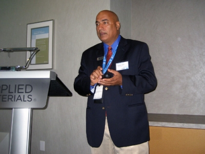
Randir Thakur speaks to the press at Applied Materials.
AMAT’s parking lot is covered with a solar panel roof.
Click to Enlarge
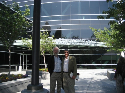
Dick James, Chipworks, poses with journalist Dave Lammers in front of the Applied Materials building.

"Precisely engineered" interfaces.

# Thakur (pictured at right) says, "RTP, EPI, CMP, inspection, CVD and PVD tools integrated in MTC."

# Avenir is already "tool of record" for leading logic and foundry 22nm.

# Tablets like iPad key new app driving flash memory. Going to see enormous growth in coming months.

# Products: need to scale platform, have no software problems and deliver on the wafer.

# 50x feature size reduction in last 20 years on Endura.

# 60 of new etch chambers at customers.

# Producer Avila low temp TSV other new product.

# 30k ft2 MTC has 120 tools include full TSV process line.

# April 23, 1990: first Endura. 2000: 300mm. Virtually every microchip in last 20 yrs produced on Endura, says AMAT.

# Avenir RF PVD: capable of 10A layers almost equivalent to ALD. RFPVD = less damage during gate stack formation.

# RFPVD can deposit both metals and metal oxides. Two options: gate first or gate last. First has 3-4 metal layers; Last has 7-8.

# R&D Endura for MG has 7 chambers incl ALD, CVD, RFPVD (3 of the latter).

# Avenir has 87% bottom coverage.

# Avenir: TiN for PMOS and TiAl for NMOS to achieve different work functions. 4.2 vs 4.9 eV.

# Centinel RE-ALD enables thinner diffusion barriers. No chlorine, low temp, halogen-free process.

# Via middle or via last two options: either can be done at wafer fab; via last done at OSATs. AMAT offers tools ‘cept bonding and grinding.

# Sesh Ramaswami: 3D packaging started with cameras then stacked memory, gaming consoles and now networking.

# Post bond-to-carrier processes need to be low temp.

# Competition announced a way to reduce Cu overburden by etch; AMAT says it doesn’t create overburden so no need to remove.

# Thermal budget less than 200°C post bonding. AMAT has doe "quite a bit of integration work" in this area.

# Avila combines throughput and low temp in Producer dual chamber system for isolation liner, backside seal and CMP stop and passivation.

# Isolation liner hermetic comp to 400°C PECVD process.

# RDL passivation process also developed with incl "seamless" passivation of Cu bumps.

# Up to 3× throughput and >30% lower CoO compared to competing systems, says Ramaswami.

#    More than 25 customer integration lots have been processed in 2010. Glass carriers also supported. 

Sign up for Pete Singer’s twitter at http://twitter.com/PetesTweetsPW

Get more news, podcast interviews, and videos from SEMICON West at http://www.electroiq.com/index/Semiconductors/semiconwest2010.html

Read about AMAT’s 5 new products, listen to a podcast interview about the AdvantEdge Mesa etch system, and watch a video interview about the product launches here: http://www.electroiq.com/index/display/semiconductors-article-display/7651049861/articles/solid-state-technology/semiconductors/industry-news/technology-news/2010/july/applied-materials.html

(July 15, 2010) — Alok Vaid of GlobalFoundries, explains the technology in his paper on time-to-solution for scatterometry metrology. Scatterometry takes a long time, but Vaid proposes a new approach with more automation.

More from Global Foundries at the show:
Global Foundries lays out road-map for advanced silicon
AMD spin-off Global Foundries has been detailing how it will overcome the technical challenges of mass producing silicon hardware at 28nm and beyond.
Read the story from SEMICON West at http://www.electroiq.com/index/display/semi-wire-news-display/1222823641.html

Get all the latest news, podcasts, videos and more from SEMICON West at http://www.electroiq.com/index/Semiconductors/semiconwest2010.html

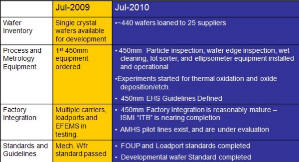
July 14, 2010 – In its closed-door session during SEMICON West, the International SEMATECH Manufacturing Initiative (ISMI) presented an update on the steps it is taking this year to provide the needed infrastructure, and momentum, to enable an eventual transition to the 450mm wafer size — from 450mm silicon readiness to factory integration issues, test wafer generation, process and equipment readiness, and equipment testing methodologies. SST got a few snippets from these meetings, courtesy of Tom Jefferson, ISMI’s 450mm program manager.

  • Test wafer development has started for multiple process and metrology equipment. ISMI is soliciting proposals for 450mm equipment for test wafer generation and demonstration — and supplier interest is increasing.
  • Silicon suppliers are in position to provide additional quantities of 450mm wafers, with "improved quality."
  • Standards are completed for 450mm FOUPs and loadports, and 450mm mechanical and developmental-grade wafers.
  • Automated mechanical handling systems (AMHS) prototype pilot lines are currently under evaluation.
  • Equipment platforms are becoming available; strategy for equipment demonstration testing are defined.


Click to Enlarge

450mm progress, 2009-2010. (Source: ISMI)

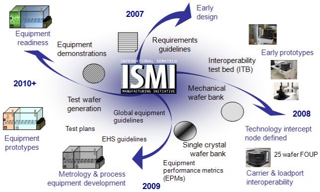
ISMI continues to drive activities required to enable the needs of its members to realize a cost-effective 450mm transition — and 450mm readiness continues to accelerate and gain momentum "in all segments of the supply chain," notes Jefferson. Key challenges and goals include creating a comprehensive 450mm infrastructure at advanced technology nodes; and continued "constructive discussion" with companies who want to contribute toward the consortia’s 450mm transition goals.

Click to Enlarge

Coordinating industry convergence toward 450mm. (Source: ISMI)


by Mike Fury, Techcet

Click to EnlargeJuly 14, 2010 – The first day of SEMICON West 2010 kicked off with a keynote address by IBM’s Bernie Meyerson, who has become a perennial favorite at the podium. His talk, "From Ghz to systems to solutions; our industry in transition," provided some insights on how Moore’s Law is morphing from device scaling to system scaling. Along the way, additional attention is being focused on enabling global IT networks while still leaving enough spare electrical power for us to operate our hybrid cars and HDTV home entertainment systems. It’s a shame that keynote addresses so often command the broadest audience but are most frequently the very talks for which slides are not available to attendees.

Rob Rhoades, CTO at Entrepix, reports that they’ve been seeing a lot of requests for refurbished CMP tools from non-CMOS clientele, for applications including MEMS, TSV, LED and other compound semiconductors. The consumable materials for these non-standard processes are still being adapted from available semiconductor product lines, as these market opportunities are still generally regarded as too small to justify customized product development.

Marty Mason at Vantage Technology gave me a quick tour of their real-time, undiluted CMP slurry particle monitoring system. Slurry flows through the system at 30 ml/minute and produces a real-time histogram of particle size distribution from 0.9-9.9μm, with the ability to go as high as 20μm. There is some additional capability at the low-end as well, though this seems to be of more interest to slurry developers than to line engineers.

Speaking of CMP, the NCCAVS has scheduled sessions during SEMICON West for the CMP User Group (Wednesday 1-5pm), and on Thursday for the Junction Technology Group and the Plasma Applications Group (both 11am-3pm). AVS is also sponsoring the International Conference on Planarization/CMP Technology (ICPT) in Phoenix, November 14-17.

Pat Levy at Pall Microelectronics gave me a quick tour of their latest filter product introductions. For CMP slurry applications, the Profile Nano Filter is a multi-layer web of melt-blown nanofibers about 50% smaller than their previous generation. In addition, while earlier products were spec’d at the cartridge level, this product line is spec’d at the level of individual filter media layers. The net result in performance on both silica and ceria slurries was a 30% decrease in microscratch defects on the polished wafer surface, compared to their prior generation filter. For broader fab applications, a new generation of filters for surface preparation applications is the Ultipleat line, made with polyarylsulfone rather than a Teflon-related backbone. This allows particle capture to 10nm vs. a 20nm minimum for Teflon. The filter media also incorporates a pore size asymmetry from one side to the other, providing for maximum particle capture with minimum pressure drop, and therefore high fluid flow rates. This product line is intended for functional surface prep chemistries line DHF, BOE, and even more aggressive agents.

Woo Sik Yoo, CTO at WaferMasters, had an unmet metrology need for characterizing the results of wafer thermal processing in their hot wall, isothermal processing chamber. Sometimes you just have to invent something yourself to meet that need, but coming up with a suite of three unique measurement tools is a sure sign of an over-achiever. WaferMasters is introducing their metrology products this week. These include multi-wavelength Raman and photoluminescence, and an optical surface profilometer. These can produce both chip-scale and wafer-scale results.

Ceimig Ltd. of Dundee, Scotland, has shown up with the Scottish Enterprise group of small companies and startups. Several suppliers already provide ALD precursors for BKM tool recipes. Ceimig is a step further back in the R&D pipeline, offering custom synthesis of organometallic compounds for evaluation as ALD precursors, with a focus on platinum group metal compounds. For emerging semiconductor applications, this includes such favorites as Hf, Ru, and Ir.

The folks at Megasonic Sweeping. are very pleased with the level of interest they are receiving for their batch cleaning megasonic transducer tanks. The bulk of their business is in retrofit kits for 200mm wafer tanks. This caught my attention because it is yet another indicator that, in this industry, we are very quick to predict the demise of old technologies but rather slow to bury any bodies. I worked on megasonic cleaning at IBM in the 1980s, and since then obituaries have been posted many times over both for batch cleaning and for wet cleaning. Both seem to be alive and well — like their other zombie cousin, optical lithography.

In wandering the show floor, the astute observer may notice that the floor today is smaller than the floor of years gone by. Many of the nooks and crannies once filled by smaller booths are empty. Several meeting venues have been moved onto the main show floor, instead of being held in closed conference rooms. It remains to be seen if this open environment is suitable for all of the meetings, if for no other reason than the background noise and distractions from casual passers-by. I will be able to judge this for myself, at the aforementioned NCCAVS CMPUG session Wednesday afternoon on the Moscone South TechSITE stage.

On a personal note, I am very gratified by the number of folks who have asked me if I would be blogging on this SEMICON show, as they’d seen my MRS, ECS, and IITC blogs and had come to expect more. As I understand it, this is how crack dealers establish their clientele, starting with free samples and then increasing their expectations. Unfortunately, I have no good ideas how to monetize this as effectively as a crack dealer does, and am open to suggestions.


Michael A. Fury, Ph.D, is senior technology analyst at Techcet Group, LLC, P.O. Box 29, Del Mar, CA 92014; e-mail [email protected].

(July 14, 2010) — Mark Allison, VP, Strategic Marketing, Verigy Ltd., points out that the economic downturn helped promote the outsourced semiconductor assembly and test (OSAT) model, which pushes test platforms into more configurable models. Verigy also announced new test products at SEMICON West.

Play Now or Download

Listen to more podcasts from SEMICON West, watch videos, and get all the latest SEMICON West news.

Verigy Showcases New Test Technologies at SEMICON West 2010
Verigy (NASDAQ:VRGY), a premier semiconductor test company, will showcase its newest products, present two technical papers and take part in an executive summit panel at the SEMICON West trade show, July 13-15 at the Moscone Convention Center in San Francisco.
Get the product information here: http://www.electroiq.com/index/display/semi-wire-news-display/1221216235.html