Category Archives: Semicon West

(July 13, 2010) — Advanced Micro-Fabrication Equipment Inc. (AMEC) is fielding interest from packaging companies in the Primo D-RIE tool, which can be used to etch wafers for through-silicon via (TSV) interconnects.

At SEMICON West 2010, AMEC highlighed its rising market momentum across Asia. Since its debut at SEMICON Japan 2007, the company has positioned its advanced dielectric etch tools at five tier-one customer fabs in three Asia regions. The installations include repeat orders for AMEC’s Primo D-RIE tool, which is being used by customers in production at nodes of 65 nm and 45 nm, and below. New tools are on order and slated for shipment throughout the remainder of the year. More recently, the system’s productivity, reliability and cost-of-ownership advantages have drawn the attention of packaging companies seeking a high-end yet cost-efficient etch solution for emerging thru-silicon via (TSV) applications. AMEC intends to leverage its technology in this space and is already working with packaging customers in China.

Given the order momentum, and to further exploit the supply-chain cost efficiencies that enable the company to provide best-in-class, low CoO solutions, AMEC will expand its manufacturing capacity beyond its Chinese facilities into other Asia locations. 

The announcement coincides with the SEMICON West tradeshow in San Francisco. This year’s show is upbeat, with industry trade association, SEMI, recently forecasting that worldwide Fab spending for 2010 is expected to approach over $36 Billion, which represents year-over-year growth of about 117 percent. This figure includes the construction and equipping of front-end facilities.

The upside trends favor AMEC’s rising momentum in the Asia market. The company’s traction validates the strength of its core etch technology and highlights the appeal of an Asia-based supplier to Asia-based semiconductor companies. More importantly, it provides clear evidence that industry leaders are relentlessly seeking high-end tools that exceed technical and performance expectations for very advanced processing, but come with an affordable price tag. For these leaders, commanding healthy margins as they migrate into the 22-nm processing realm means teaming with supplier partners who understand their technical and economic priorities. AMEC’s technology and product roadmap is in sync with this migration and the company continues to refine its offering with technical and productivity enhancements to provide the optimum economic solution for customers at these leading-edge nodes.

“AMEC is greeting the upturn with a pragmatic but diversified technology and market strategy,” said CEO Gerald Z. Yin, Ph.D. “In the last two years, we’ve stayed on course in spite of challenging industry conditions and a global economic downturn. We surpassed key milestones, which included successfully positioning our Primo D-RIE tool at customer sites and closing a $46M Series D funding round earlier this year. Since our inception in 2004, we have raised more than $190M from venture capital sources. We appreciate our customers’ confidence in our technology and their partnership as we worked to refine our product. We’re looking forward to further expanding our installed base and market footprint.”

Advanced Micro-Fabrication Equipment Inc. (AMEC) is a semiconductor equipment company with proprietary wafer fabrication solutions. To learn more, please visit www.amec-inc.com.

Get the latest SEMICON West 2010 news and first-hand accounts at http://www.electroiq.com/index/Semiconductors/semiconwest2010.html

(July 13, 2010) — In this video, LaMar Hill, North East Sustainability Institute, State University of NY, talks about renewable energy and motivating a younger generation of engineers. Senior technical editor Debra Vogler speaks with Hill at the Advanced Semiconductor Manufacturing Conference, taking place in San Francisco with SEMICON West this week.

To get all of the latest news, videos, podcasts, and more from the show, visit http://www.electroiq.com/index/Semiconductors/semiconwest2010.html

(July 13, 2010) — The Soitec Group (Euronext Paris) released the Ultra-Thin Buried Oxide (UTBOX) extension to its Ultra-Thin (UT) silicon-on-insulator (SOI) platform, a robust substrate solution for chip designers tackling the performance, power and density challenges of mobile consumer devices.

Fully Depleted (FD) planar body transistors are now recognized as the right path on the CMOS roadmap for the 22nm generation and beyond. With FD planar transistor technology on UTBOX wafers, chip designers can enhance their usual design flows and techniques. High-volume capacity is available for the 22nm node at Soitec’s manufacturing sites in France and Singapore.

With an ultra-thin, insulating buried oxide layer, system-on-chip (SOC) designers and system architects can leverage standard techniques for attaining lower power and higher performance as needed by the target applications. The UTBOX option further complements the existing advantages of planar FD technology, which solves transistor variability issues, delivers the best device electrostatics, and enables SRAM to operate at lower supply voltages (Vdd). It is an evolutionary and highly manufacturable technology that offers simple processes and continuity of design tools, leading to a very cost-effective solution.

For FD planar to live up to its promise, the starting wafers must meet very stringent top silicon uniformity specifications. With ultra-thin top silicon thickness variation within a ±0.5nm maximum range, and a buried oxide layer as thin as 10nm, these wafers are in full compliance with customer requirements.
"FD SOI is the right technology at the right time. As the challenges to control bulk leakages become very expensive and unreliable, FD SOI offers a simple solution. Additionally, the fact that FD SOI is a planar and scalable technology with no history effects provides a seamless design transition. This is a powerful combination," said Horacio Mendez, executive director of the SOI Industry Consortium.

Paul Bodre, Soitec, discusses performance and design roadblocks for mobile app system on chip (SoC). Wafer manufacturing with buried oxide technology is an enabling technology. 

The Soitec Group provides engineered substrate solutions for microelectronic products. Three other divisions, Picogiga International, Tracit Technologies and Concentrix Solar, complete the Soitec Group. For more information, visit www.soitec.com. Soitec is exhibiting in booth #1333 in Moscone Convention Center’s South Hall at the Semicon West trade show, July 13-15 in San Francisco.

See all the latest coverage from SEMICON West here: http://www.electroiq.com/index/Semiconductors/semiconwest2010.html

(July 13, 2010) — ASML Holding NV (ASML) announced broad customer adoption of holistic lithography products that optimize semiconductor scanner performance and provide a faster start to chip production. All of ASML’s leading-edge scanners are now sold with one or more holistic lithography components.

Semiconductor manufacturers face increasingly smaller margins of error as they shrink chip features. Holistic lithography provides a way to shrink within these margins to continue Moore’s Law. Introduced a year ago at SEMICON West 2009, ASML’s holistic lithography suite of products enable continued shrink and provide customers with higher yield, sooner. Holistic lithography integrates computational lithography, wafer lithography and process control to optimize production tolerances and reduce “time to money” for chip makers. ASML customers have adopted multiple products from the holistic product portfolio into research & development (R&D) as well as volume manufacturing. Products like Source Mask Optimization (SMO), FlexRay, LithoTuner, Baseliner and YieldStar are in use worldwide.

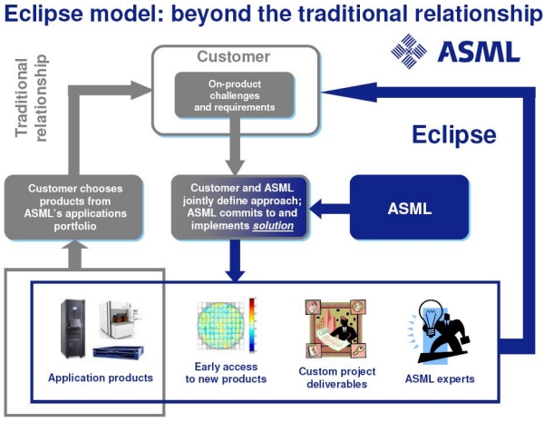
ASML also offers holistic lithography as an integrated package called Eclipse, which is tailored to a specific customer, node and application, and which enables maximum performance at chip making and ramp to volume production at the earliest possible time. A significant number of ASML’s advanced customers have adopted an integrated Eclipse package.

Click to Enlarge

“Most chip makers have found that, for current and future process nodes, independent optimization of process steps is insufficient. The entire litho process must be integrated and co-optimized for the best performance. Eclipse extends the capabilities of their hardware and helps them to produce chips with smaller geometries,” said Bert Koek, senior VP, applications product group at ASML. “With detailed knowledge of our scanner characteristics and interfaces we can work closely with our customers to integrate computational lithography solutions during R&D, and implement customized improvement targets during manufacturing.”

Customers who have adopted Eclipse are seeing the results. STMicroelectronics for example will incorporate Eclipse in conjunction with a TWINSCAN NXT:1950i scanner for their 28-nanometer (nm) node. The key deliverables of the package are on-product specifications for both overlay and critical dimension uniformity (CDU). The 28-nm Eclipse package for ST includes a full range of products from ASML, including scanner tuning products, immersion scanner application, stabilization and conditioning; and the ASML applications support to achieve the specified targets. Preparations for Eclipse at the next node have started with a feasibility study on 20nm critical layer printing options.

“To optimize development cycle times and manufacturing solutions for 28-nm and beyond, ST is working with ASML to define targets, processes and design parameters,” said Joel Hartmann, technology R&D group VP and GM advanced CMOS, derivatives and eNVM technology, STMicroelectronics, at Crolles, France. “ASML’s Eclipse packages include application products, custom project deliverables and application support that enable joint process optimization.”

Holistic lithography approach

The semiconductor industry is driven by shrink that reduces manufacturing cost and improves device performance. However, as semiconductor feature sizes shrink, so do process windows – the accuracy tolerances necessary to produce viable chips – imposing extremely tight requirements on parameters such as overlay and critical dimension uniformity (CDU). Independent optimization of separate parameters is no longer sufficient and holistic lithography intelligently integrates computational lithography, wafer lithography and process control.

During the chip design phase, ASML’s holistic lithography uses actual scanner profiles and tuning capabilities to create a design with the maximum process window for a given node and application. Once in manufacturing, ASML holistic lithography optimizes a scanner for a specific pattern or reticle, and monitors and controls litho-cell overlay and CDU performance over time to continuously maintain the system centered in the process window. Integrated into the Eclipse suite of products are:

  • FlexRay uses a programmable array of thousands of individually adjustable micro-mirrors. It can create any pupil shape in a matter of minutes – eliminating the long cycle time associated with diffractive optical element (DOE) design and fabrication and thus accelerating ramp to yield for low k1 designs.
  • Tachyon SMO co-optimizes and analyzes scanner source and mask design simultaneously, ensuring an optimized process window from R&D through production while minimizing pitch and number of exposures per layer.
  • BaseLiner enables optimized process windows and higher yields by keeping scanner performance to a pre-defined baseline condition.
  • YieldStar offers a single sensor solution for CD, overlay and sidewall angle metrology resulting in high-speed, high precision and high-accuracy measurement.
  • LithoTuner optimizes the scanner in an application specific manner. By combining device pattern information and scanner specific characteristics, the optimum setting for maximum process window and flexibility will be determined.

ASML provides lithography systems for the semiconductor industry, manufacturing complex machines that are critical to the production of integrated circuits or chips. For more information, visit www.asml.com

See all the latest coverage from SEMICON West at http://www.electroiq.com/index/Semiconductors/semiconwest2010.html

by Debra Vogler, senior technical editor

July 12, 2010 – Applied Materials unveiled its latest conductor etch solution, the Centura AdvantEdge Mesa, in advance of SEMICON West. Thorsten Lill, VP of etch applications & technology development in the company’s etch and clean business unit, summarized the drivers for the new product: double-patterning and 3D devices, which drive uniformity, selectivity, and aspect ratio dependent (ARDE) requirements at advanced nodes. Whether horizontal device scaling (double-patterning or new mask materials), or vertical device scaling (such as 4F2 DRAM cells, complex post-NAND stacks, or FinFETs), etch becomes more complicated, e.g., as the etch goes deeper, the etch rate slows down, and depth control is impacted.

Applied tackled the problems inherent with advanced conductor etch by synchronizing plasma pulsing, instead of using continuous wave plasma. (Lill explains the physics behind the innovation, called Pulsync, in a recorded podcast interview). When pulsing the source and bias power synchronously, one has to ensure very good plasma stability and chamber matching, he notes. “When you turn off the source and bias at the same time, the plasma starts to relax, the charged species start to recombine and end up on the structure of the wafer or chamber walls and you get a different kind of chemistry in the plasma,” he said. “In the off-cycle, we get a larger number of molecular species and these tend to have less energy per ion, which translates into intermetal selectivity which we’ve shown with 8Å gate oxide recess.” By turning off the plasma, the structures have the opportunity to discharge. “A charged structure increases the ARDE because it deflects the ions. By turning off the plasma, you can neutralize the surface and start fresh, which results in a 3X better ARDE” compared to continuous wave plasma.

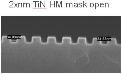
According to the company, Pulsync also reduces both intra-cell and dense-to-isolated loading for <3X nm. Additionally, the company says that it has demonstrated sub-1nm gate oxide recess. Uniformity performance is shown in the figure below.

Click to Enlarge
AdvantEdge Mesa uniformity performance. The source delivers 1% depth uniformity and sub-1nm CD uniformity. (Source: Applied Materials)


(July 12, 2010) — Alchimer S.A., a provider of nanometric deposition technology for through-silicon vias (TSV), semiconductor interconnects, and other electronic applications, announced that Panasonic Corporation (NYSE: PC) has become an equity investor in the company.

“Throughout the electronics supply chain, manufacturers are increasingly in need of high-quality nanometric metal films that can be mass-produced at low cost,” said Patrick Suel, venture partner with Panasonic Venture Group. “We see this at the wafer level, on substrates, and in 3D packaging, which is emerging as an important technology to lower costs for future ICs and systems. We believe that Alchimer’s nanometric films have tremendous potential to change the traditional cost-performance ratio at many points along the value chain.”

Alchimer’s breakthrough technology, electrografting (eG), is an electrochemical process that enables the growth of extremely high quality polymer and metal thin films on both conducting and semiconducting surfaces. The company’s deposition technology reduces overall cost of ownership for high-aspect-ratio TSV metallization by up to two-thirds compared to conventional dry processes, and shortens time to market. 

In addition to electrografting, Alchimer has developed chemical grafting (cG), an electroless process sequence that enables the growth of highly adherent, low-resistivity copper-diffusion barrier films on isolating surfaces through the formation of strong chemical bonds between the films. 

Funding has been facilitated by the Panasonic Venture Group, a Silicon Valley-based unit of global consumer electronics leader Panasonic R&D Company of America, which invests in companies that may present a technology-based advantage to Panasonic. Through its investments, Panasonic Venture Group champions technology partnerships between private companies and R&D units of Panasonic. The dollar amount of the investment and Panasonic Venture Group’s equity holding were not disclosed.

 “The Panasonic Venture Group is known for its investments in companies that present potential strategic competitive advantages to Panasonic, and we are very pleased to have them as an investor as we commercialize our technologies,” said Steve Lerner, CEO of Alchimer. “We believe that electrografting offers substantial promise as an enabling technology for TSVs and 3D interconnects, which we expect to move quickly into high-volume production in the next few years.”

Alchimer develops and markets innovative chemical formulations, processes and IP for the deposition of nanometric films used in semiconductor interconnects and 3D TSVs (through-silicon vias), as well as other applications in the electronics value chain. Visit the company at SEMICON West in San Francisco this week, Moscone Center, South Hall, Booth 1811.

Get all the latest news from SEMICON West at http://www.electroiq.com/index/Semiconductors/semiconwest2010.html

July 11, 2010 — With continued device geometry and new process steps comes increasing use and variety of CMP steps — e.g. through-silicon vias (TSV), ceria used for shallow-trench isolation, very thin interlayer dielectrics, colloidal silica for copper steps, copper barrier steps. These also mean an increasing need to find and eliminate (or better yet, prevent) wafer defects and yield losses, including particles. Newer slurries being introduced and used in chemical mechanical planarization (CMP) are more densely packed with particles that can cause defect and damage and impact processing yield, and it’s a challenge to find them — both small and larger ones. Enter Vantage Technology, which is debuting at this week’s SEMICON West (South Hall, booth #425) a new slurry particle measurement technology, SlurryScope (patented in the US and internationally), to provide undiluted real-time measurement of industry-standard production slurries.

Often fabs measure highly diluted samples of their slurry (e.g. Ceria or colloidal silicas) to collect data on particle size distribution. Quantifying the impact of damaged/scrapped wafers due to CMP slurry agglomeration is difficult to divine, but it’s often in the top-10 pareto of wafer processing among leading IC and foundry operations, explains Marty Mason, EVP of sales and marketing — from 2%-3% yield impact up to 10% for newer designs, and applications requiring multiple finished wafers (e.g. TSV) compound the problem of any scratches or defects. And current equipment can’t measure those slurries due to high large particle counts (LPC) in a mean range (mostly <1μm) of abrasive particles. Some LPCs are known to be "soft" (i.e., no impact to the process), vs. the "hard" LPCs that can cause grooves, gouges, etc. — but without knowing the entire mechanisms behind all LPCs, the safest step is to get all of them out, a problem for CMP suppliers, Mason noted. "We don’t have a good understanding of what the LPCs actually are" — larger versions of the "good" desired abrasive particulates, or are they agglomerations, or even contaminants? Do they form when the slurry is shipped or stored, or run through certain pumping systems? Are they in all slurries?

Conventional slurry monitoring systems have to significantly dilute (>>100×) ceria and colloidal silica to measure particles, and generally they still can’t measure large particle counts, explains Mason. "They can only take small sample amounts from large batches [50-100mL] of slurry, and hope that it represents the bulk of the slurry," he explains. "But we measure it all, as it flows through" — without any dilution — and provide particle size distribution of the slurry with each snapshot of integration (~2-10sec). Existing tools to determine particulates in CMP slurry have "been around for years," employing tactics like light scattering, laser diffraction, etc. — methods that all break down and can’t measure heavy thick slurries. Dilution hasn’t really solved that problem, because that affects not just the particle count but also pH, stability, and reliability.

Vantage’s answer: measure the slurry in real-time as it goes to each and every wafer, and correlate the data to the exact wafer, not just a sampling every few hours. This constant monitoring (up to 300ml/min ) can help flag any high counts before too many wafers get impacted. "You can see the trend of particles vs. wafer results, wafer by wafer, how large particle count changes might impact wafer yield, damage, scratching, etc." Toolmakers like this idea, he points out, because it can show that the slurries — and not the processing tool — is responsible for any damage or loss. That also means more responsibility/risk shifted to slurry suppliers…some of whom have been receptive to Vantage’s monitoring technology; others, not so much.

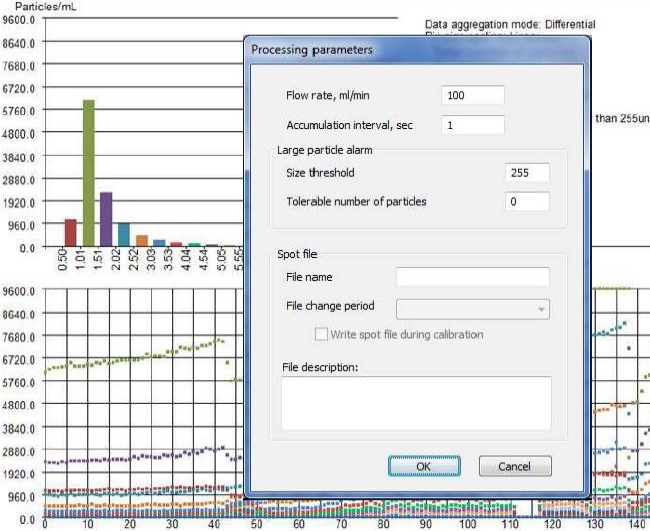
The company’s SlurryScope shows a real-time plot of bin sizes counting the number of particles every few tenths of a second, and a historical summary of bins over time as the slurry flows past (Figure 1). Users can set up an "alarm threshold" of bin activity (silicas hardly ever change, but colloidal and ceria particle counts "can move around," Mason notes). Others have also tried to develop systems that better identify and track undiluted slurries in real-time, but one had problems managing buildup (requiring stoppage and cleaning, making it impractical) and the other wasn’t able to achieve results repeatedly, Mason said. Vantage claims to avoid the buildup problem with its flow-through process (not periodic samples) and flushing with DI water; other parts of its technology involve "different techniques on light and optics that haven’t been used before," but Mason declined to discuss them, except to invoke some patents assigned to the company’s CTO Rashid Mavliev.

Click to Enlarge

Figure 1. SlurryScope software interface. (Source: Vantage)

The San Jose-based company has been working jointly with "select customers" in IC manufacturing, slurry makers, and IC/foundry operations to develop "a closed-loop approach" to slurry monitoring to protect wafers from large particles, and to track variations in slurry particle distribution and correlate them to wafer yields. Mason said the company has received "good interest" from multiple customers in the US and Asia, taking samples from both IC and slurry companies. So far data collection has been in the subfab where slurry distribution lies come from the tank and go out to the fab area — not on the platen at actual production, which will require a lot more integration of monitoring with IC company’s database, and other types of CMP-related measurements already being taken coming in and going out of tools (e.g. removal rate, uniformity, particles). Entering this workflow at the point before slurry hits the wafer — "that’s where we need to go next," Mason said.

One potential customer expressing interest in collaboration is SVTC — both to help collect and monitor data for their development customers but also the equipment companies. It also helps that with SVTC’s customers, most of whom are still at early development, "they don’t use a whole bunch of unique slurry, just what the customer gives them, e.g. off-the-shelf stuff," he added.

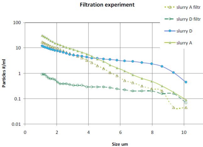
Mason also identified another area of benefit for the CMP monitoring system (Figure 2). "If we identify LPCs to avoid damage, it’s a payback" to customers, Mason noted. "But if we show them how to extend filter lifetimes, that’s another payback" — either slashing the cost of filters, or revealing if a filter needs to be changed more often. — J.M.

Click to Enlarge

Figure 2. Effects of filters on particle measurement. (Source: Vantage)


In the future, the production of advanced LED structures is expected to grow more rapidly with the growth in energy efficient, long-lifetime luminaries for general lighting applications. In this article, we will outline the most important measurement capabilities that allow the rapid and reliable control of the LED production process using HRXRD, and the latest advances in HRXRD technology to allow true in-line monitoring. This article includes a video interview with Jordan Valley Semiconductors from SEMICON West 2010.

Paul Ryan, John Wall, Richard Bytheway, David Jacques, Kevin Matney, Qu Bo, Jordan Valley Semiconductors UK Ltd, Belmont, Durham, UK

Key parameters for the quality of advanced LEDs are the wavelength and brightness of the emitted light. Several structural parameters control these aspects, and these have traditionally been determined using high resolution X-ray diffraction (HRXRD).

A typical HB-LED structure is based on III-nitride materials and is dominated by a repeating unit of InGaN and GaN layers. These two, thin layers are repeated several times (typically between five and 10 repeat units) to create a multi-quantum well (MQW). This MQW is the heart of the LED structure, and the details of the MQW structure determined using HRXRD play a key role in the success of the device. In particular:

1. The In composition within the InGaN layer, along with the number of repeats within the MQW, the wavelength of the light can be controlled;

2. The repeatability of the thickness of each layer within the stack is critical for efficient MQW structures; and

3. The mosaic tilt and twist of the structure controls the efficiency and yield of the device

In this video from SEMICON West, Isaac Mazor, Jordan Valley Semiconductors, talks about LED structures and the LED market: the green/eco drivers, high investment in capacity, energy savings, etc. LED applications go side-by-side with semiconductor fab applications.

Measurement of In composition and MQW thickness

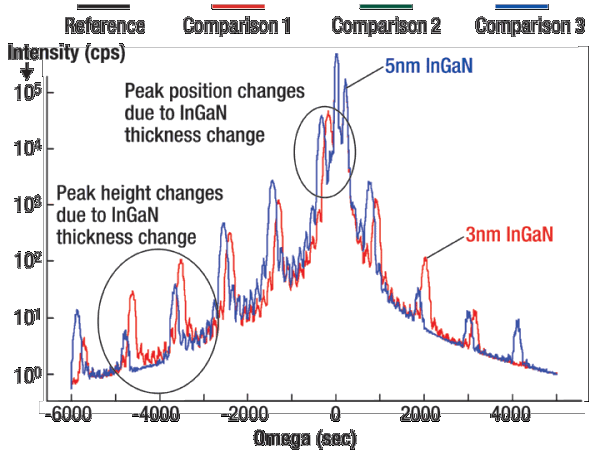
A perfect LED structure, with a MQW repeat of 15nm and a 15% In composition, would give a HRXRD pattern as shown in Fig. 1. The general diffracted intensity consists of a narrow, intense peak from the GaN buffer layer (centered at 0s in the figure), another peak to slightly higher angle of the GaN, which is attributed to the AlGaN layer. The position of this peak is related to the Al content within the AlGaN layer, and the height, and width, of this peak is related to the thickness of the AlGaN layer.
Click to Enlarge
Figure 1. The effect on the HRXRD spectrum by varying just the InGaN layer thickness.

The series of peaks from the MQW structure give a large amount of information about the layer thicknesses and composition within the MQW:

1. Satellite period gives the combined thickness of the InGaN and GaN (bilayer repeat thickness); and

2. The position of main MQW peak gives the average In composition within the InGaN / GaN pair (note, this is not the In composition within the InGaN layer).

To determine the actual In composition within the InGaN layer, a number of other factors must be considered, namely the individual InGaN and GaN layer thicknesses within the MQW, and the relaxation of the MQW structure relative to the GaN buffer layer. We will consider the case where the layers are assumed to be relaxed, as is often historically assumed within production.

There are two main affects on the data when the InGaN thickness is changed, as shown in Fig. 1. First, the MQW to substrate peak separation increases, as the average composition within the MQW has increased by increasing the InGaN thickness relative to the total GaN + InGaN thickness. Second, the period of the satellite peaks remains unchanged, but the ratio of peak heights varies with the InGaN thickness. Therefore, to enable the InGaN layer thickness, and hence the In composition, the data must cover several satellite peaks and the simulation software must accurate fit to the satellite peaks over a wide angular range. It should be apparent that a high intensity incident beam and low baseline is required in order to reliably determine these key structural parameters.

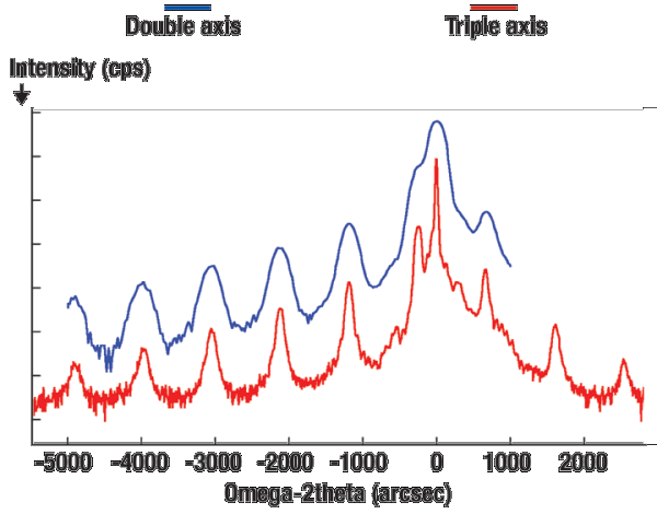
In the examples above, the structures are assumed to be structurally perfect. However, the growth of GaN is typically dominated by a mosaic structure. This mosaic structure has a major influence on the HRXRD spectrum. The peaks are broadened as the mosaic tilt essentially smears out the details of the diffraction pattern. This leads to the main MQW peak being merged into the main GaN peak, as shown in the blue spectrum in Fig. 2, preventing accurate analysis of the In composition. However, the data is still suitable for bilayer thickness analysis.
Click to Enlarge
Figure 2. Comparison of HRXRD spectra collected with and without triple axis analyzer crystal, from an MQW structure with mosaic tilt.

To enable accurate and precise measurements of the key MQW parameters the influence of the mosaic tilt must be minimized within the HRXRD data. This is achieved by inserting an analyzer crystal in front of the detector in order to improve the angular resolution of the measurement without substantially reducing the intensity. This then allows high-quality diffraction data to be obtained, as seen in the red spectrum (Fig. 2). Advances in X-ray measurement techniques allow these measurements and automated analysis to be performed in a few seconds on production HRXRD monitoring systems, such as the QC3 tool.

Traditionally, HRXRD has often been used for process development applications using a traditional R&D diffractometer, typically requiring a manual configuration of the system with long data collection times and tedious analysis of the data. However, dedicated production optimized HRXRD systems are now available that have specifically designed to address many of these issues at a low cost of ownership. The QC3 system, for example, allows triple axis scans to be performed in less than one minute. It allows for automated configuration of the system, wafer alignment and full structural analysis in parallel with subsequent measurements. Results can be output in a variety of formats and customized for statistical process control SPC.

Conclusion

For the accurate determination of In composition, and hence wavelength, high quality diffraction data with high intensity, low background that span wide angular ranges are necessary, and full dynamical simulation is required for detailed analysis. This requires a high intensity source with a high dynamic range detector.

The latest generation of HRXRD tools specifically for production monitoring are designed to be able to determine the key structural parameters for LED analysis on multiple wafers in a single batch run, with a simple user interface suitable for a production environment.

Biographies

Paul Ryan received his BSc and PhD from the U. of Leeds, UK and is VP Corporate and UK Site Manager at Jordan Valley Semiconductors UK Ltd, Belmont Business Park, Belmont, Durham, UK; ph.: +44 191 332 4700; email  [email protected].

John Wall is R&D Manager at Jordan Valley Semiconductors UK Ltd.

Richard Bytheway received his BSc from the U. of Wales, Swansea, UK and is a technologist at Jordan Valley Semiconductors UK Ltd.

David Jacques received his D.E.A and Diplome d’Ingénieur from Institut National des Sciences Appliquées de Toulouse and is a product manager at Jordan Valley Semiconductors UK Ltd.

Kevin Matney received his BS and MS from UCLA and is a senior technologist at Jordan Valley Semiconductors Inc.

Qu Bo received his PhD from the Institute of Semiconductors, CAS and is a regional applications manager for Asia at Jordan Valley Semiconductors UK Ltd.

More Solid State Technology Current Issue Articles
More Solid State Technology Archives Issue Articles