Category Archives: Materials and Equipment

June 13, 2011 – BUSINESS WIRE — International Rectifier, (IR, NYSE:IRF), power management technology provider, introduced a PQFN 2 x 2mm with <1mm profile package featuring its latest HEXFET MOSFET silicon. The new package is ultra-compact, high density and efficient for lower-power applications such as smart phones, tablet PCs, camcorders, digital still cameras, notebook PCs, servers, and network communications equipment.

The new packages add to IR’s power MOSFET packaging options, miniaturizing form factor with benchmark silicon, said Stéphane Ernoux, director, IR’s Power Management Devices Business Unit, adding that they suit applications with high digital content.

The new PQFN2x2 devices are available in 20, 25, and 30V with standard or logic level gate drive, using IR’s latest low voltage N-Channel and P-Channel silicon technologies to offer very low on-resistance (RDS(on)), and high power density in line with a PQFN3.3×3.3 or PQFN5x6 package.

The PQFN2x2 family includes P-Channel devices optimized for use in the high-side of load switches, providing a simpler drive solution. They are RoHS compliant.
 
International Rectifier (NYSE:IRF) provides power management technology via analog and mixed signal ICs, advanced circuit devices, integrated power systems and components. For more information, go to www.irf.com.

Also read: Power semiconductor packaging drops wire bonding for sintered foil

Subscribe to Solid State Technology/Advanced Packaging.

Follow Advanced Packaging on Twitter.com by clicking www.twitter.com/advpackaging. Or join our Facebook group

By Debra Vogler, senior technical editor

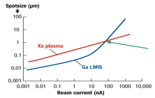
June 13, 2011 — FEI launched its Vion plasma focused ion beam (PFIB) system based on inductively-coupled plasma (ICP) source technology using a xenon ion beam. The system generates more than a micro-amp of beam current and can remove material faster (>20× improvements in speed, Fig. 1) than liquid metal ion sources that typically max out at a few tens of nano-amps, according to the company. Because of its speed, FEI will target new technologies, such as 3D packaging and 3D transistor design technologies, where PFIB analysis is more practical.

Click to Enlarge
  • High-volume milling/high beam current
  • Ga-FIB loses size advantage to plasma source as beam current goes above 50-60 nA
  • Xe has high sputter yield, high brightness, and low energy spread
  • No Ga contamination

Figure 1. Plasma FIB is 20× faster than current FIBs. Its fast ion milling capabilities enable rapid cross-sectioning of features from 50-1000µms. SOURCE: FEI

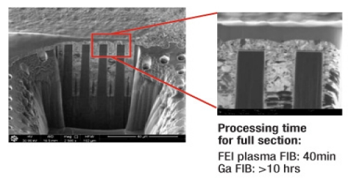
In a podcast interview, FEI product marketing manager Peter Carleson explained that gallium FIBs are already used for packaging applications, but with the cross-sections and trenches necessary for such applications (in the neighborhood of ~100µms), the removal process can take three, four, or even 8 hours. With the new source’s higher beam current, more samples can be done with greater tool utilization. The PFIB can also access lower regions of stacked dies to do traditional failure analysis or debugging (with the device "on") on the devices in the lower regions. The PFIB also enables quicker cross-sectioning of 3D integrated circuits that use TSVs/interposer layers (Fig. 2).

Click to Enlarge

Figure 2. High-speed sectioning of TSVs with plasma FIB. The device was located, cross-sectioned, polished, and imaged with PFIB. SOURCE: FEI

The product can perform site-specific removal of package and other materials to enable failure analysis and fault isolation on buried die; and circuit and package modifications to test design changes without repeating the fabrication process or creating new masks. Other applications include process monitoring and development at the package level, and defect analysis of packaged parts and MEMS devices.

Listen to the podcast:


  • Format: mp3
  • Length: 4:29
  • Size: 4.10 MB
  • Date: 06/13/11

June 9, 2011 — Yole Développement’s "Thin Wafer Manufacturing Equipment & Material Market" research study found at least 10 methods currently in use to temporarily bond wafers, protecting thinned wafers during processing.
Click to Enlarge
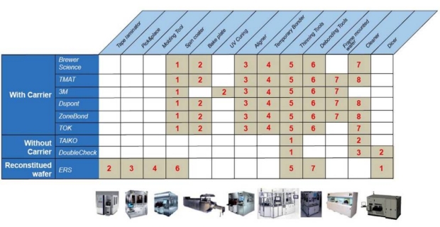
Figure. Temporary bonding tools used during a temporary bonding step. The figures in red show the order of the steps. Source: Yole, Thin Wafer Manufacturing Equipment & Materials Markets Report, June 2011.

Many consumer applications will require ultra-thin semiconductor wafers (down to 50µm) for advanced packages with through silicon vias (TSV), interposers, or fan-out wafer-level packaging (FOWLP); power devices like IGBTs, RF devices, and LEDs. Because ultra-thin wafers are less stable and more vulnerable to stresses than traditional ones, and die can be prone to breaking and warpage during grinding and wafer processing, new temporary bonding technologies will be required for handling support.

Wafer bonding tapes are unsuitable for ultra-thin wafers: they cause non-uniformity, can impact flexing, etc.

Yole has identified at least 6 carrier-based temporary bonding technologies — each with variations in chemistry, carriers, etc. Add to that carrier-free adn reconstituted wafer technologies, and the options are 10 or more. The market is so young, and no options are clearly winning out over others, says Dr Eric Mounier, Project Manager at Yole Développement, which means the technology developers are competing to win converts.

Companies mentionned in the report:

3M, ABB, Accretech, AIT, All Via, ALSI, AMAT, Brewer Science, Corning, Danfoss, Denka, Disco, DoubleCheck Semiconductors, Dupont, Dynatex, ERS, ESI, EVG, Fairchild, FhG IZM, Fico, Furukawa, Hamamatsu, Hitachi Chemical, Infineon, Invensense, IR, Jenoptik, Laserod, Leti, Lintec, Loadpoint, Lumileds, Mitsui Chemicals, Nitronex, Nitta, Nitto Denko, OnSemi, Osram, Panasonic, Plan Optik, ProTec, PVA Tepla, RFMD, Ricmar, Rorze, Schott, Scrypt, Sekisui, Shibuya, ShinEtsu, Skyworks, STM, Strasbaugh, Sumitomo Bakelite, Sumitomo Chemical, SUSS MicroTec, Synova, Sysmelec, Takada, TEL, TMAT, TOK, Triquint, Veeco, Yushin

The goal is temporary wafer bonding at a low cost, with high temperature resistance and no or little topographic issues. Tool makers, chemistry providers, and substrate suppliers are all working together in various ways to reach that goal. A few — Nitto Denko, TOK or TEL — are attempting to be a process and chemistry provider.

Yole expects the temporary bonding market to experience 5x market growth 2011 to 2016, raising its value to $300 million. Wafers that require temporary bonding during processing will top 35M by 2016 (estimated across all wafer sizes).

"Thin Wafer Manufacturing Equipment & Materials Market" describes markets, applications and technologies for thin wafer manufacturing: temporary bonding markets, applications, descriptions and trends for wafer thinning and dicing. This report also includes a market analysis on temporary bonding materials (wax, glue, tapes, carrier wafers) associated with the temporary bonding technology.

Dr. Eric Mounier has a PhD in microelectronics from the INPG in Grenoble. Mounier is in charge of market analysis for MEMS, equipment & materials at Yole. 

Yole Developpement is a market research and strategy consulting firm analyzing emerging applications using silicon and/or micro manufacturing. Learn more at www.yole.fr  

Subscribe to Solid State Technology/Advanced Packaging.

Follow Advanced Packaging on Twitter.com by clicking www.twitter.com/advpackaging. Or join our Facebook group

June 9, 2011 — Nordson Corporation (NASDAQ:NDSN) opened a demo center in Dongguan, China for customers of its Advanced Technology Systems operating segment. Nordson ASYMTEK, Nordson DAGE, and Nordson YESTECH brands will be represented in equipment demonstrations, application engineering support, training, sales, and service.

Click to Enlarge
Nordson leaders celebrate the opening of the company’s newest facility in China. From left to right: Leyu Louis, Sales & Business Development Manager (Bondtester Division) Nordson DAGE; Greg Wood, Vice President, Nordson Advanced Technology Group, Asia; and Frank Wang, General Manager, Greater China Nordson ASYMTEK


The Nordson brands provide dispensing, coating and testing for high-technology and related sectors. South China’s advanced manufacturing base is growing, and the Dongguan facility adds to Nordson’s China-wide presence Beijing, Shanghai, Guangzhou and Suzhou, said Greg Wood, VP, Nordson Advanced Technology Group, Asia.
 
Nordson ASYMTEK provides precision automated fluid dispensing, conformal coating, and jetting technologies.

Nordson DAGE manufactures high-resolution x-ray inspection and bond testing equipment for analyzing the integrity of electronic connections in semiconductor packages and printed circuit board assemblies.

Nordson YESTECH designs and manufactures automated optical inspection and x-ray inspection systems for yield enhancement in electronic assembly industries.

Subscribe to Solid State Technology/Advanced Packaging.

Follow Solid State Technology on Twitter.com via editors Pete Singer, twitter.com/PetesTweetsPW and Debra Vogler, twitter.com/dvogler_PV_semi.

Or join our Facebook group

June 8, 2011 — Semikron developed a power semiconductor packaging technology, SKiN, which uses flexible foil and sintered interconnects instead of bonding wires, solders, or thermal paste. Current density is doubled — 3A/cm2 compared with 1.5 A/cm2 with standard wire bond technology — and load cycle capability increases 10x. Converter volume can be reduced by 35%.

Click to Enlarge

The SKiN sintered foil replaces the wire bonding on the chips, and the underside of the chip is sintered to the DBC substrate. The sintered layers have a lower thermal resistance than solder interconnects, and connect the chip across its full surface, improving thermal management. A sinter layer replaces the thermal paste layer and the soldered base plate.

Semikron expects the technology to be used for vehicle and wind power semiconductors, including SiC and GaN devices. The packaging technology enables use in higher operating temperatures with improved reliability over traditional power devices, according to the company. When SKiN packaging is used, a 3MW wind power converter can be fit into a single switch cabinet; a 90kW converter for hybrid and electric vehicles can be 35% smaller than the smallest converter currently available. For converters in vehicles and wind power units, liquid-cooled systems are used.

Semikron is a power semiconductor manufacturer. Learn more at www.semikron.com.

Subscribe to Solid State Technology/Advanced Packaging.

Follow Advanced Packaging on Twitter.com by clicking www.twitter.com/advpackaging. Or join our Facebook group
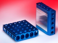
June 7, 2011 — JaroThermal’s Honeycomb heatsink directs heat towards the outside of the device, while Click to Enlargeproducing a steady flow of cool air inside the heatsink. Honeycomb heatsinks can be used with either plastic or metal/ceramic BGA packages, depending on the thermal interface material (TIM).

The design is studded with holes, helping increase surface area and cross ventilation. Ambiant air is cooled even as heat is released.

Applications include video cards, motherboards and networking applications. The design is thin, suiting compact, low-profile designs.

JARO’s adhesive mounted version eliminates the need for mounting holes in the PCB.

Jaro Thermal provides electronics thermal management technologies. Learn more about the product at http://www.jarothermal.com/honeycomb.pdf (PDF)

Click to Enlarge

Also read: Cooling high-power packages by Kaveh Azar, Ph.D. Advanced Thermal Solutions

Subscribe to Solid State Technology/Advanced Packaging.

Follow Advanced Packaging on Twitter.com by clicking www.twitter.com/advpackaging. Or join our Facebook group
June 7, 2011 — FSI International Inc. (Nasdaq:FSII), surface conditioning equipment supplier, won orders for multiple ORION single wafer cleaning systems. A memory maker will use the ORION in wet photoresist strip and etch and a foundry will use it for backend-of-line (BEOL) processes, like cleaning film stacks.

Click to EnlargeThe orders were received during the third quarter of fiscal 2011 and are expected to ship in the second half of calendar 2011.

The memory producer will use the FSI system for front-end-of-line (FEOL) wet photoresist strip and middle-of-line (MOL) metal etch applications. FSI cites a memory fab conversion from batch immersion to single wafer technology as one reason for the order, saying that single-wafer cleans improve defectivity and cycle time performance. The ORION system offers short process times and integrated atomized spray bar.

The foundry producer will use the system for back-end-of-line (BEOL) cleaning processes. Foundry and logic manufacturers are finding low-k materials and metal film stacks much more sensitive to wet cleaning than previous BEOL process generations, FSI notes. The closed chamber technology of the ORION system has demonstrated highly efficient removal of etch and ash by-products without causing galvanic corrosion or changes in metal and dielectric film properties.

FSI International Inc. is a global supplier of surface conditioning equipment technology and support services for microelectronics manufacturing. For more information, visit FSI’s website at http://www.fsi-intl.com and the ORION product page at http://www.fsi-intl.com/index.php/applications-and-products/orion-single-wafer-cleaning-system

Subscribe to Solid State Technology/Advanced Packaging.

Follow Solid State Technology on Twitter.com via editors Pete Singer, twitter.com/PetesTweetsPW and Debra Vogler, twitter.com/dvogler_PV_semi.

Or join our Facebook group

May 31, 2011 — What’s driving the semiconductor industry to new materials R&D methods? Combinatorial methods, high-productivity development tools, can shorten development times: getting to success or failure faster. Mike Besnard, ATMI, speaks with senior technical editor Debra Vogler at The ConFab 2011 in Las Vegas.

Listen to Besnard’s interview:

"The cost of R&D is going higher and higher every year," Besnard says. If combinatorial science can improve process technologies and manufacturing methods, new nodes can be less expensive; lowering the cost of advancing materials.

As the semiconductor industry goes to smaller and smaller nodes, is it possible to improve the combinatorial platform? Besnard says that, as you understand tool requirements, you can evolve the combinatorial platform to screen materials and also hardware. The correlation from development to high-volume manufacturing (HVM) really involves an interplay of materials and tool science, Besnard points out.

Combinatorial research compresses dozens to hundreds of experiments onto one wafer, with each processed individually. Learn more about it in these articles: 

Click to EnlargeIn an exclusive series of blogs, imec reports from its International Technology Forum (ITF) last week in Brussels. Els Parton, science editor, imec, shares Jy Bhardwaj’s (Philips Lumileds) points about LEDs costs improvements.
 
May 31, 2011
— LEDs currently appear in applications where performance — color, brightness, light quality — defines a compelling advantage over conventional light bulbs. A few barriers still stand between LEDs and mass adoption in illumination. "First, there is the cost (lumens per dollar) that has to decrease by a factor 10 if LEDs want to be competitive with conventional bulbs. This 10x cost reduction will be achieved by both performance and cost improvements. More in detail, this will be achieved by increasing the internal quantum efficiency (IQE) at high drive current, by improving the Phosphor conversion and by increasing the wafer size with yield and scale enhancement," Jy Bhardwaj, vice president technology R&D at Philips Lumileds Lighting Company, explains.

The second barrier to be overcome is light quality, states Bhardwaj. How do you achieve a consistent, controllable shade of white? An important research topic to tackle this problem is getting a good control of the phosphorous layer (density and thickness) in the LED stack. "Our company has come up with a new device architecture that enables this. It’s a thin film flip chip architecture for InGaN LEDs,"explains Bhardwaj.

Bhardwaj predicts that it will take another 3 years to achieve the desired 10x cost reduction. And by 2020, 80% of our planet’s lighting will come from LED.

Bhardwaj’s colleague Iain Black at Philips Lumileds recently spoke to Solid State Technology’s The ConFab audience about LED manufacturing improvements. Read his points about LED costs improvements via manufacturing here.

Els Parton, science editor, imec, and colleagues are blogging exclusively for Solid State Technology and its ElectroIQ.com partners from imec’s International Technology Forum (ITF) last week in Brussels.


Read more blogs from imec’s ITF:


Subscribe to Solid State Technology/Advanced Packaging.

Follow Solid State Technology on Twitter.com via editors Pete Singer, twitter.com/PetesTweetsPW and Debra Vogler, twitter.com/dvogler_PV_semi.

Or join our Facebook group

May 31 2011 — RJR Polymers, high-performance air cavity package (ACP) developer, will debut liquid crystal polymer (LCP) semiconductor packaging technology for RF and microwave system designers at the International Microwave Symposium (IMS2011). RJR’s new product is competitive with ceramic ACPs, improving thermal management and offering design flexibility based on the company’s epoxy range. 

The company is currently offering two thermally-enhanced, metal-based ACP platforms for radio frequency (RF) power and quad flat-pack no-lead (QFN) applications.

Designers can use copper or various other metal bases in the new package, selecting RJR’s epoxies and epoxy-coated lids to meet design-specific requirements. Thermally efficient power transistor packages need to handle higher-performance devices now, said Wil Salhuana, president and CEO, RJR, noting that designers still require flexibility for their systems.

The three-piece package can include materials with high thermal conductivity and components with higher co-efficient of thermal expansion (CTE) mismatch. The modular product line uses a standard molding process and creates a flat seal surface. RJR says this manufacturing technique creates one-third the dielectric found in ceramic and copper leads. By creating a single injection mold and simply swapping out the lead frame, LCP ACP users can use the same package for diverse products with lower design overhead and development time than creating new packages for each iteration.  The packaging technology can be built to all industry standard configurations or modified for custom designs.

RJR will be available to discuss this innovative packaging technology at IMS2011 in booth 718. The IEEE Microwave Theory and Techniques Society (MTT-S) International Microwave Symposium covers all of the latest developments in microwave technology from nano devices to systems applications, June 5-10 in Baltimore, MD.

RJR Polymers, Inc. develops air cavity LCP semiconductor packaging, epoxies, epoxy-coated lids and sealing equipment for RF, cellular, automotive, optical, imaging, and sensor applications, as well as new solar power, high-power LED, and highly integrated system-level applications. For more information, visit www.rjrpolymers.com.

Subscribe to Solid State Technology/Advanced Packaging.

Follow Advanced Packaging on Twitter.com by clicking www.twitter.com/advpackaging. Or join our Facebook group