Category Archives: Semicon West

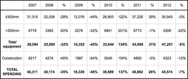
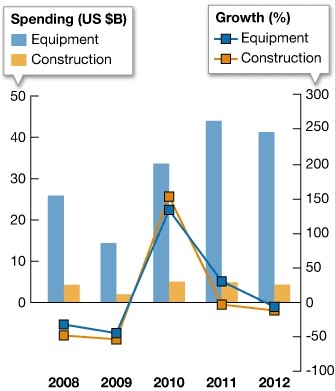
June 8, 20111 – The semiconductor industry’s torrid pace of capital equipment expenditures will continue in 2011, but actual construction of new fabs is slowing to "historically low" levels, according to data from SEMI.

Some companies in 2011 have already increased their guidance for capital spending (most notably Intel), which should help push total fab equipment spending to a record $44B this year, says Christian Gregor Dieseldorff, senior analyst of fab information in SEMI’s Industry Research and Statistics group. Spending in 2012 will dip slightly (-6%) to $41B, he predicts.

But in stark contrast to equipment spending, actual fab construction is slowing down significantly, and that could spell trouble for capacity plans in 2012 and beyond, he warns. 17 new volume fabs have "a high probability" (>60%) of beginning construction this year, but 13 of those are for LEDs — only four volume semiconductor fabs are slated to break ground this year. And in 2012, only another four chip fabs are on the boards. SEMI also is now calculating who is looking to build out 450mm facilities, with construction beginning last year and more in this year.

Installed capacity should rise about 9% this year and another 7% in 2012 and (excluding discretes) is leveling off to <10% annually, according to Dieseldorff. (The Japan earthquake/tsunami/nuclear/recovery odyssey won’t have a significant impact on installed capacity, minus some possible short-term effects on utilization and output, he adds.) Foundry capacity growth surpassed memory fab capacity in 2010 and should do so again in 2011 (13% vs. 8%), while LEDs continue to race ahead in with double-digit growth (40% in 2011). Memory still dominates with 38% of installed fab capacity, trailed by foundries (29%).

The fab spending and construction forecasts will be part of a joint SEMI/Gartner market symposium at SEMICON West, on Monday afternoon July 11.


Click to Enlarge


Click to Enlarge

 Spending on equipment (new and used) by wafer size, and construction, in US $M.
*Number rounded (Source: SEMI World Fab Forecast, May 2011)


by Dr. Paula Doe, SEMI Emerging & Adjacent Markets

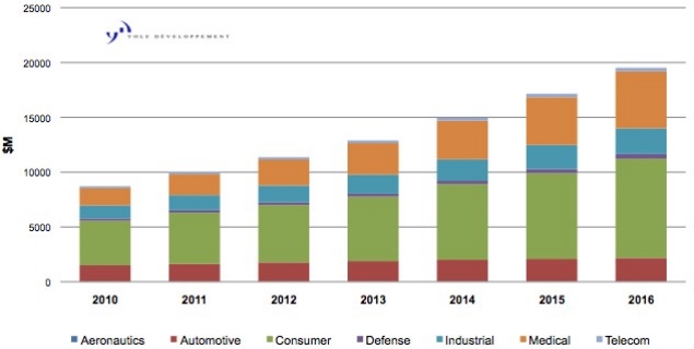
June 7, 2011 – Rapid growth in mainstream consumer markets is changing the structure of the MEMS industry from an artisanal to a volume manufacturing business. Yole Développement projects the MEMS market will near the $10 billion level this year, and is poised for 14% compound annual growth for the next five years, to approach close to $20 billion by 2016.

Click to Enlarge
MEMS forecast per application. (Source: Yole Développement)

These volume markets demand more efficient, non-artisanal solutions for moving designs into production. At the same time, with the maturing of the basic manufacturing technology, the value is moving from the device to the function and the system. And all these developments create a new set of challenges and opportunities to companies to find better ways to speed the ramp to low-cost volume production, to find better ways to integrate multiple die and software into easy-to-manufacture and easy-to-use functions, and to find the right business models to best use these skills to succeed.

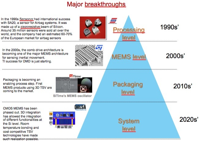
There has been a steady evolution over time, notes Yole founder and CEO Jean Christophe Eloy, as the young MEMS industry has matured to delivering higher functionality, from the manufacturing of MEMS structures in the 2000s, to the more recent innovations in integrated packaging. Coming next will be innovations in wafer bonding and through-silicon via (TSV) integration of multiple sensors and controls, requiring both packaging expertise for the integration and software expertise for managing the complex sensing and actions to be useful — raising the question of who in the value chain will do these steps.

Click to Enlarge
30 years of MEMS manufacturing history, an evolution aimed at climbing the value chain
toward increasing functionalities at the system level. (Source: Yole Développement)

The demand for rapid ramp to high-volume production is driving manufacturers to focus increasingly on ways to more efficiently re-use established process stacks or technology platforms or even product platforms for the more efficient development of new products. And the need to reduce cost for consumer products is driving a relentless push to smaller die size, and to integration by TSV or wafer bonding when possible, and to solutions like capping the MEMS with the ASIC or making use of SOI to form the cavity, says Eloy.

GlobalFoundries’ Rakesh Kumar, director of MEMS, argues that there’s big potential to apply an IC foundry’s best known methods and practices — worked out after many years of experience in semiconductor tools and technologies — toward the more efficient manufacturing of MEMS. To be successful, an IC foundry must lower costs, offer high yield and high-performance MEMS products in a manner similar to ICs, while also shortening time-to-market by reduced technology transfer time and fast ramp to production, he says.

Specialty MEMS foundries are also developing solutions. Claude Jean, EVP/GM at Teledyne DALSA Semiconductor, suggests that the traditional MEMS approach of developing products first on lab equipment then porting over to manufacturing tools is too slow for fast ramp to yields and fast cost reduction. Instead, he highlights the advantages of doing the final rounds of development with an infrastructure closer to production tools.

IMEC’s Jo De Boeck, SVP of smart systems and energy technology, suggests that MEMS technology platforms are required, supported with a design environment consisting of a reference tool flow, corresponding models and design kits and a basic design IP library. Moreover, successful product innovation implementation will require co-developing software and hardware into optimal systems solutions.

We’ve invited these speakers representing leading companies from different viewpoints across the value chain — as well as ones from major IDM Robert Bosch and startup Sand9 — to discuss these key industry issues at SEMICON West, Tuesday, July 12 ("The Future of MEMS". Right afterwards, for a more hands-on look at the future of MEMS, the MEMS Industry Group presents a demo zone of next-generation MEMS sensors in action, demonstrated by MEMS folks who can give the inside scoop on how they work.

Tuesday afternoon also features a related program focusing on packaging issues for heterogeneous integration of MEMS and CMOS. Microsoft’s GM of packaging, quality and reliability, Raj Master, will give the technical keynote, followed by an update on market trends from TechSearch International and IHS iSuppli, and a panel discussion including Fraunhofer IZM, Toshiba Corp. and CEA-Leti, moderated by Analog Devices and NIST.

by Denise Rael, FlexTech Alliance

May 25, 2011 – Recent progress on developing printable conductive inks, flexible substrates, and associated continuous processes for making electronics means there’s now an advancing infrastructure ready for the practical manufacture of disruptive new products. Utilizing a collaborative community of individuals and leading technology companies, FlexTech Alliance has identified, funded, and directed advanced development in the flexible and printed electronics infrastructure. New technology enables circuitry that is conformable and able to be mass-produced, from low-cost integrated intelligence in packaging to new types of displays, building-integrated solar, and wide-area lighting panels.

One step toward moving these research technologies into practical production is reliable information on materials properties that clearly specifies just how these properties are measured, so users can make an informed comparison of like products. To this end, Western Michigan U. (WMU) has created a user-friendly database of materials properties and information on their processing (by manufacturing platform). There are many new developments to be added to this knowledge base. For instance, a new series of copper-oxide reduction inks for inkjet and screen printing from NovaCentrix report sheet resistances as low as 60 mΩ/sq on paper substrates with ink costing less than $100/kg in volume.

Additionally, progress in post-print processing for drying, sintering, and annealing printed inks to improve their functionality is enabling higher performance for more demanding applications. NovaCentrix has developed a method utilizing high-intensity flash lamps to heat the functional films but not the substrates, potentially allowing solution-based processes for photovoltaics and displays. Another approach uses pulsed flash lamp technology for low-temperature sintering of nanoparticle inks in roll-to-roll (R2R) processes. Xenon offers Xenon Flash lamps that are capable of delivering very high peak energies over a very short duration of a few milliseconds, allowing faster and more effective sintering in high-speed R2R processing compared to low-temperature bake ovens. This low-temperature solution has shown no substrate degradation on a number of different substrates.

These latest developments in printed electronics materials, tools and processes will be discussed in greater depth at the Extreme Electronics TechXpot session "Printed electronics: Beyond R&D to real-deal technologies," presented by FlexTech Alliance at SEMICON West, July 14, 2011. WMU, NovaCentrix and Xenon are members of FlexTech Alliance. For more information about FlexTech Alliance visit www.flextech.org.

May 12, 2011Solid State Technology and SEMI are pleased to present the 2011 Best of West product awards program. It is the first time that the two groups are co-hosting the awards program. The Best of West Award is given to recognize important product and technology developments in the microelectronics industries.

The Best of West Award will spotlight exciting new products and technologies at SEMICON West, which attracts 25,000 attendees in July in San Francisco. SEMICON West exhibitors are encouraged to enter their new (introduced after SEMICON West 2010) products for the semiconductor, photovoltaics/solar, micro-electromechanical systems (MEMS), LEDs/solid state lighting, and printed/flexible electronics markets. All exhibitors are encouraged to participate.

Winners will be selected by an independent panel of highly qualified judges. Best of West finalists and award recipients will be selected based on the submission’s financial impact on the industry, engineering or scientific achievement, or societal impact and benefits.

The fine print:
Consideration for the Best of West awards will be limited to all products, services and technologies publicly introduced from August 1, 2010 to SEMICON West 2011. Submitting companies must be developers of the product or technology (no rep firms or third parties) and must be exhibitors at SEMICON West. SEMI reserves the right to make all final decisions on eligibility. Entries are limited to two per exhibitor.

Finalists will be selected by vote from a distinguished panel of judges from academia, industry and SEMI. Finalists will receive recognition for their achievement through press releases, on the SEMICON West website, through online exhibitor directories, and special booth displays.

Winners will be announced during SEMICON West and will be selected from the pool of finalists. Judges may visit exhibitors during SEMICON West to obtain further information on the submission.
 
Submit an entry:
To submit entries for consideration, complete the online form at http://dom.semi.org/web/wevals.nsf/callforinnovators2011?openform.

In addition to company name and contact information, a maximum 750-word description of the new product/technology is required, along with a max. 300-word summary of why it’s important, submitted in Microsoft Word. Supporting charts, graphs and illustrations must be submitted as part of the Microsoft Word document. Entries that are not submitted in Microsoft Word or otherwise do not follow the above instructions, will be rejected for consideration.

Award submissions are due June 17, 2011.

Subscribe to Solid State Technology/Advanced Packaging.

Follow Solid State Technology on Twitter.com via editors Pete Singer, twitter.com/PetesTweetsPW and Debra Vogler, twitter.com/dvogler_PV_semi.

Or join our Facebook group

Farewell, Selma Uslaner


September 21, 2010

It is with great sadness that I report the passing of longtime Solid State Technology editor, Selma Uslaner, on September 20th. The news was relayed by Sid Marshall, son of the late Sam Marshall. Sam and Selma were the first editors of SST in the late ‘50s (Sid later joined SST as editor-in-chief and then associate publisher and editorial director of Solid State Technology, as well as founding editor and publisher of Microlithography World).

Selma’s contributions to the industry and the magazine are legendary. Selma worked on the magazine since its inception in 1958. Her various roles included editorial assistant, show coordinator, reporter, news editor, managing editor, and director of industry relations. 

Her 50 year milestone at SST was celebrated at Semicon West in 2007. SEMI’s Stanley T. Myers came to shake her hand, as did many well-known industry friends and associates. As Gail Flower reported at the time, many attendants talked about Selma as an "industry maverick," a person who groomed a generation of women in electronics to be tough when needed and to say what they thought. Her industry associates were said to be part of Selma’s Sorority. "There’s a certain chemistry that takes place when you do what you love to do," said Selma. "I’ve loved this magazine since its inception. Now I have lots of grand friends in the industry." Her articles have helped fledgling industries and start-up companies grow considerably. "There’s always an incredible but true story of someone in the electronics industry who built something in his garage, and that’s just where it all starts," she said. She thanked everyone for honoring her and added that she wished she could live into the next century to see what her industry guests would come up with in the future.

I see no more fitting tribute than to simply provide an excerpt of words that Selma herself penned, which appeared in the May 1997 issue of Solid State Technology, in a historical look back at the Industry’s “Golden Age,” of which she was so much a part.

“This year, Solid State Technology celebrates four decades of technology coverage of an amazing industry. We look back at its early years, not to lament the passing of bygone times often called "those good old days," but to commemorate the privilege of chronicling the birth and incredible technological advancement of an exciting new industry that has revolutionized our lives.

“Two major events of the year 1956 were the re-election of Dwight D. Eisenhower as President of the US, and the awarding of the Nobel Prize in physics to three American scientists – Drs. William Shockley, John Bardeen, and Walter Brattain, – who invented the transistor in 1947 at Bell Laboratories in Murray Hill, NJ.
At about the same time, Sam Marshall, a young visionary editor at a small publishing company in New York City, had begun to develop the concept of a semiconductor trade magazine. He visited various companies, met with industry people to assess their needs for reportorial coverage of their technical achievements, and planned the scope and editorial direction of the publication. In January 1958, after the semiconductor industry had crossed the $100 million mark, the bi-monthly Semiconductor Products (Solid State Technology`s original title) made its debut. Early technical contributors to the new magazine included industry giants Bill Shockley, Andy Grove, and H.C. Lin, among others.

“In his charter issue`s editorial, Sam laid out the magazine`s editorial purpose and objectives: "to provide current and authoritative information pertaining to the semiconductor industry and to the scientific personnel engaged in this industry; to provide a medium for scientists to transmit their ideas, developments, and investigations; and to provide a reportorial service wherein we will present helpful facts, figures, and information from authoritative sources." He further stated, "The articles and papers appearing in this magazine are intended to be on an engineering level, covering basic R&D, application, and production of semiconductors and other solid-state devices, as well as their related products. First and foremost will be the kind of article that will help the engineer in research, design, and production problems." A few examples were given of the ever-growing applications of transistors. Sam went on to say, "As the versatility of solid-state devices becomes more and more apparent, their applications will become more universal. We have barely scratched the surface of development and application in this new and exciting industry." How right he was!

“Those, of course, were the days long before faxes and desktop computers. Magazine copy was set by linotype. Layouts were done on a table with rubber cement. Sam solicited and edited the technical manuscripts, and I edited and proofread the news and product sections. Most of the news in the industry, all in the US in those days, came in via the US mail and telephone. I took many company announcements over the phone in longhand so that manufacturers could meet our deadline and make the next issue. Galleys were mailed to authors for checking, a means of communication we called "pony express." My electric typewriter (the first in the company) served as "office automation." In its second year of publication, Semiconductor Products became a monthly. Oscar Fisch, Sam`s teaching colleague and a physicist by education, joined the staff to primarily assist with editing the technical feature articles.

“During those early years as a neophyte editor, I came into contact with many brilliant young engineers when Sam sent me to cover industry events. I called that time my "Did I know…" period. Did I know that history was being made? Did I know, on one such occasion, that a young man sitting on the floor during an informal press meeting and talking about very little that I understood, would become an industry icon? His name was Robert Noyce. Did I know?” Selma Uslaner

Farewell, Selma. R.I.P.
(August 13, 2010) — In this video interview, Bryan Rice, SEMATECH, discusses the readiness of EUV. SEMATECH is partnering with Carl Zeiss for EUV process development. The next phase will be a blank inspection phase, beginning a few months after SEMICON West. Bryan speaks with senior technical editor Debra Vogler.


EUV was a major topic of conversation at SEMICON West 2010. Learn more in these video interviews on advanced lithography:

Research updates on EUV, mask, cleaning, etc from Leti: http://www.electroiq.com/index/display/semiconductors-article-display/1122585507/articles/solid-state-technology/semiconductors/lithography/2010/july/research-updates_on.html

EUV news from SEMICON West with Toppan Photomasks: http://www.electroiq.com/index/display/semiconductors-article-display/8262574301/articles/solid-state-technology/semiconductors/lithography/2010/july/euv-news_from_semicon.html

ASML: Exposure tool development for EUV: http://www.electroiq.com/index/display/semiconductors-article-display/0567969896/articles/solid-state-technology/semiconductors/lithography/2010/july/asml_-exposure_tool.html

Also read:

Lithography trends at Sokudo breakfast forum at http://www.electroiq.com/index/display/semiconductors-article-display/7993765989/articles/solid-state-technology/semiconductors/lithography/2010/july/semicon-west__lithography.html

and SEMICON West Lesson #2: Capital intensity & EUV at http://www.electroiq.com/index/display/semiconductors-article-display/0883314816/articles/solid-state-technology/semiconductors/industry-news/technology-news/2010/july/semicon-west_lesson.html

and visit the semiconductor lithography center from Solid State Technology at http://www.electroiq.com/index/Semiconductors/lithography.html

(August 11, 2010) — Jennifer Braggin, Entegris, chaired a session at ASMC, co-located with SEMICON West in San Francisco in July, on defect inspection. In this video, she summarizes the key points: new processes and materials add new detection challenges, and analysis from the lab is now moving into the fab. Wafer-edge inspection is highlighted.

Learn more about wafer inspection at our semiconductor inspection center: http://www.electroiq.com/index/Semiconductors/inspection.html

Read more about Entegris here: http://www.electroiq.com/index/search.html?si=eiq+&collection=eiq&keywords=entegris

(August 2, 2010) — In this video interview with senior technical editor Debra Vogler from SEMICON West 2010, James Moyne, Applied Materials (AMAT), highlights a new technology: virtual metrology. Virtual metrology, on which Moyne presented at ASMC/SEMICON, enables tighter semi fab control using line data analysis. The summarized data is synched with real metrology data. Virtual metrology, a technique that has been around for a while, is now adaptive. Moyne explains.

Read more about semiconductor wafer inspection here: http://www.electroiq.com/index/Semiconductors/inspection.html

Also read: EDA interface value proposition from SEMATECH, 10/2008
Cycle-time improvements and time-waste reduction are being accomplished by improving equipment setup times and operations. Realizing even greater efficiency, however, requires the use of more sophisticated means of collecting data and controlling the equipment …

Visit the SEMICON West 2010 center on Solid State Technology: http://www.electroiq.com/index/Semiconductors/semiconwest2010.html

(July 30, 2010) — In this video interview from SEMICON West 2010, Christopher Wargo, Entegris, talks contamination control at 22nm and below. Lithography presents a suite of issues for contamination control. While the technology exists to confront new contaminants, commercialization is key. Wargo speaks with senior technical editor Debra Vogler.

See all the video interviews from SEMICON West on Solid State Technology’s homepage, at http://www.electroiq.com/index/Semiconductors.html#v

by James Montgomery, news editor

July 29, 2010 – Over the past few weeks, industry watchers have been nudging up their forecasts to suggest at least 30% growth in semiconductor sales this year. Ahead of this pack has been IC Insights’ Bill McClean, who’s been optimistic for growth since last year. At a breakfast talk during SEMICON West he reiterated his 30% forecast (quarterly breakdown: 5% increase in 2Q10, 8% in 3Q, and 1% in 4Q) — but he also suggested a likelihood of surpassing that 30% with a stronger second-half performance (quarterly breakdown: 5% growth in 2Q10, 13% in 3Q, and 4% in 4Q). An unlikely pessimistic scenario suggested a dip in both 3Q (-3%) and 4Q (-10%), which would shrink 2010 growth down to 20%.

2009/2010 IC market growth rate quarterly scenarios.

But now McClean’s enthusiasm seems to have pulled back a tad. He tells SST that he’s lowered his outlook for quarterly IC unit growth to 7% in 3Q (vs. 8%) and a -4% decline in 4Q (vs. 1%). That’ll keep annual growth to 30% — still a stellar year, but slightly less optimistic than just a few weeks ago.

So what’s changed? In a word: oversupply. IC unit shipments appear to have overshot that 5% forecast for 2Q10, and some stockpiles have accumulated. "We believe there is some inventory being built up in the industry right now, especially in the application specific analog and logic segments," he tells SST. One culprit: analog ICs for cell phones were up 66% in May vs. a year ago, though in the same quarter cellphone unit sales rose only about 3% (to 303M units, roughly back to 2Q08 levels). The rise of smartphones helps soak up more chip usage, but "this type of IC unit volume increase should always raise some concern," he says. And the communications market is a good early-warning signal for inventory buildup and burnoff heading into 4Q10 and 1Q11, he points out.

2006-2010 quarterly cell phone shipments. (Source: IC Insights)

Another possible problem with IC supply is what he calls "inadvertent" inventory build. Following Apple’s iPad tablet PC introduction, no fewer than 15 companies plan to launch their own similar tablet computers — in 2H10 alone! And as is typical of a growth-market cattle call, all of them expect to capture 10% of the market (mathematically impossible of course), and they’re buying up ICs to support those aims, notably NAND flash memory and display drivers, McClean says. Once the peak holiday seasonal period is over, tablet suppliers may start to shake out, and orders for those devices "could drop significantly."

From a broader view, McClean says he is becoming more conservative as he sees IC unit volume shipments start to pull away from a long-term trendline of 9.5% unit volume growth — a line he characterizes as a rubber band held by two endpoints, and pays attention when it pulls above or below from that trend. In 1Q09 units sunk 10% below that trend line; "the worse it became, the more optimistic we were," he says. Now in 3Q10 he projects units to have snapped back above that trendline (12% higher), enough to be conversely worrisome. "The market appears a little bit overheated," he says. However, if seasonal demand for electronics keeps up strongly, there shouldn’t be excess inventory and any current buildup would be burned just to meet demand.

2000-2012 quarterly IC unit volume shipment trend.