Category Archives: Semicon West

by James Montgomery, news editor

July 26, 2010 – The issue of supply chain management came up in several keynotes, panels, and individual discussions at SEMICON West. "There’s a lot more focus on the supply chain," noted Applied Materials EVP/GM Randhir Thakur, in the Tuesday afternoon "Executive Panel." Litho tools have been getting attention as representing the worst of lead-times (9+ months, sometimes longer), but most process equipment has been straining to get product to customers — showing, more than anything, just how rapidly and completely things shut down a year ago, and how fast they’ve had to ramp back up again. (One story we heard: A major process tool firm had to pay a component partner’s delinquent electricity bill before engaging them in resupplying parts.) Thakur pointed out that some suppliers have simply shut their doors permanently.

The key, according to GlobalFoundries’ Tom Sonderman, is knowing how, where, and when to add capacity — i.e., predictability — to best manage capacity and ramp/slow as needed. That "bullwhip affects our suppliers even more so," noted fellow panelist Rick Wallace from KLA-Tencor. And one concern that comes out of this is whether quality suffers in a race to get products out the door. Lam Research now has stricter rules for its supplier base, said Steve Newberry: Lam cannot represent >40% of a supplier’s business, and the company actively pursues strategies such as multiple-qualified-supplier strategies where "basically we consider them as our own factory." Thakur agreed that quality is a fundamental issue as ramp cycles shorten — and here again, collaboration is key. "Our customers can do it; I think we in the wafer-fab equipment space can learn it," he said.

More “lessons learned” from SEMICON West 2010:
Lesson #1: Good times here, for now
Lesson #2: Capital intensity & EUV
Lesson #3: 3D and packaging are hot
Lesson #5: Interests outside CMOS

Litho has the poster child for chip tool lead-times, with reported delivery out to 9-12 months just a couple quarters ago. (It’s been suggested that Samsung’s capex surge may not only secure its own needs, but have the perhaps-not-unintended effect of keeping the critical tools out of the hands of others.) In just the past couple of months, orders in KrF tools have spiked, with lead-times rising to as much as 12 months, equal to immersion litho shipping schedules.

But things seem to be improving noticeably, due in large part to companies’ hard work to get leaner during the downturn. In the Bulls/Bears panel Q&A, Citigroup’s Tim Arcuri said ASML is on the brink of reducing lead-times to six months by September. And AMAT claims 60%-70% of its turnaround is turns business, added Goldman Sachs Jim Covello. "I’m shocked about lead-time reductions," he admitted, noting that there are more issues on the backend now. "We won’t see a level of double ordering this time." Lam’s Bagley pointed out that equipment suppliers’ lead-times always beat those of the facilities preparing to receive the tools — "it used to be a wash," he said.

That six-month lead time for immersion litho tools is actually a sweetspot, Barclays’ CJ Muse points out in his post-SEMICON West notes ("it takes 4+ months just to build a Zeiss lens). Samsung probably won’t get all the immersion tools it wants (e.g. its Austin fab may slip into 1Q11), he said. And while the NXT offers 30% better throughput, the growing number of critical layers for DRAM and logic/foundry mean more tools will be needed, not fewer, he points out.

by James Montgomery, news editor

July 26, 2010 – There was a great deal of buzz at SEMICON West about 3D ICs, thanks to down-the-street ASMC presentations and backend discussions and vendors present. Through-silicon vias (TSVs) in particular are a hot ticket — so much so that traditional frontend equipment suppliers are touting their entry. (Novellus, for example, made a splash with a suite of tools for wafer-level packaging dubbed "The New Vertical Reality," staking claim to what it says is a $700M+ market.)

(Phil Garrou also summed up several 3D/TSV presentations from SEMICON West: the TechXspot session on "Bridging the Gap," and Suss Microtec’s "3D IC Bonding and Thinned Wafer Handling Workshop.")

There are more than 15 300mm 3D IC pilot lines now, according to SEMI’s Jonathan Davis, priming the Tuesday Executive Panel’s discussion about 3D ICs. Lam’s Steve Newberry predicted the industry will see widespread adoption in 4-5 years (maybe 2-3), though standards are needed to more efficiently implement it — e.g. will it be via-first, via-last, something else? It’s also a relatively small market (a "niche" for etch, in LRCX’s view), so ROI will be tough to justify for some, and few players will be able to pay for the R&D. AMAT’s Thakur takes a broader view of 3D IC opportunities, emphasizing formfactors and performance. GlobalFoundries’ Tom Sonderman likened TSV adoption to that projected for EUV lithography, requiring collaboration and a need to identify value-adds.

More "lessons learned" from SEMICON West 2010:
Lesson #1: Good times here, for now
Lesson #2: Capital intensity & EUV
Lesson #4: Supply chain challenges
Lesson #5: Interests outside CMOS

3D and TSV offer attractive growth, but there are still questions and hype to resolve. "While front-end semicap companies were very bullish on TSV, some back-end contacts wondered aloud how TSV will reach meaningful volumes soon as some critical standards are still not formulated," writes Credit Suisse’s Satya Kumar. Citing the challenge of getting market penetration with "more capable, but also more expensive tool sets, to an end market that has traditionally used low-end, very low-cost tools," Deutsche Bank’s Steve O’Rourke projects adoption of TSVs will start in traditional wafer fabs first, then "potentially" move to backend fabs, with prices lower — "but not by much" than traditional frontend tools. Winning strategies will present "a combination of capabilities and cost of ownership arguments," he writes — but "we maintain healthy skepticism on timing and market size expectations."

Though efficiency can offer a valuable proposition, it’s hard to overstate how hugely important are costs (low) and availability (now) to backend customers. Several people with whom we talked at SEMICON West about how traditionally more frontend-oriented tool suppliers are clamoring for growth in packaging suggested it might be a tough sell, especially at the subcon level. One industry watcher said that OSATs have a simple interface point for these folks: ask them about lead-times, and if the answer is anything more than three weeks the conversation’s abruptly over. Another pointed out that in many cases, backend outsourced firms translate "lead-time" as the time it takes to walk to the dock, unwrap the plastic from one of a long bank of tools already sitting around, and plug it in.

TI’s Cu pillars

Packaging wasn’t just a hot topic among suppliers. Texas Instruments made a splash with partner Amkor, announcing qualification and production of a fine-pitch Cu pillar flip-chip package — <50μm, vs. ~150μm pitch size limitations with conventional solder-based flip chip, e.g. ball bond.

Cu pillars offer advantages over conventional solder in terms of thermal performance, better conductivity, and resistance to electromigration, as well as shorter package routing (higher pin densities, reduced die sizes). The industry is investigating their use for various reasons, e.g. as an alternative to wafer-level packages for analog devices, or replacing gold wire in some packages. Intel uses Cu pillars in its 65nm and 45nm flip-chip products (and is expected to continue through 32nm).

TI executives explained the technology is ideal for applications ranging from ASSPs (smaller body size, high pin count, low-power aspects) to DSPs (same requirements), and power management (density more than pin count) — and they’ve got customers already lined up in all three product areas. "We looked at least two other alternatives" besides Cu pillars, and "we actually built products on them, they worked fine," noted Devan Iyer, TI’s manager of worldwide semiconductor packaging. "But on the long-term roadmap, we feel like Cu pillar is the most cost-effective, the most standard in the industry."

The TI/Amkor announcement "represents one of the major adoptions outside of Intel and I believe it is the start of the wave," Jan Vardaman, president/founder of TechSearch, told SST, in conversations during and after SEMICON West. She added that she sought out the first major product known to employ the Cu pillars, a hot-selling smartphone (whose backer rhymes with "Frugal") — but found it to be sold out in the wireless provider’s store, despite a stated retail price north of $600 (without a contract).

by James Montgomery, news editor

July 26, 2010 – Everyone was in a good mood this year, and why not? Updated forecasts point to a 100%+ surge in business for many sectors of semiconductor equipment suppliers, and individually suppliers were practically beaming when talking about their current business (and increasingly, extending to end of 2010 and perhaps beyond). And semiconductor demand itself is poised for 30% growth or even more. Helping the show’s mood was Intel’s blowout quarterly numbers, and its nudge of 2010 capex up to $5.0B-$5.4B adds about $400M more to the 2010 capex pool. (That’s a far cry from Samsung’s massive spending spree, but as Deutsche Bank’s Stephen O’Rourke points out, higher spending in 2010 means there’s less chance of overspending in 2011.)

"I’m as excited as I’ve been since the mid-90s," proclaimed Novellus CEO Rick Hill, during his company’s media presentation on Monday July 12. For the past decade or more the market has been supply-driven, with companies pursuing market share. Now, there are multiple demand drivers keeping the engine humming, pointed out NVLS’ Tim Archer, following Hill on the stage — a long-overdue, global PC refresh cycle; clamor for notebooks/netbooks/tablets, and phones/smartphones. The execs projected the current upswing could last through 2012.

Most everyone is "very positive" about the near-term outlook, agreed Deutsche Bank’s Stephen O’Rourke in a research note, citing 1:1 meetings at SEMICON West with a handful of industry heavyweights.

The good news extends to other chipmakers as well, in the form of capacity announcements during the show. TI took over some 300mm fabs from Spansion Japan (and sold $40M worth of its own 300mm tools to UMC). TSMC broke ground on its third 300mm fab, Fab 15, ultimately a massive >$9B, 100,000 wafers/month behemoth — several times bigger than a typical 300mm fab — with tooling in July 2011, ramping production (40nm and 28nm) by 1Q12, and achieving full capacity by 2015. Others are prepping manufacturing as well. Satya Kumar from Credit Suisse cites "scuttlebutt on the floor" of SEMICON West that STMicro is "back on the radar" with plans to add 300mm capacity. Samsung Austin, too, may surprise with the speed of its ramp, he added, and GlobalFoundries wants to start moving tools into its NY fab "not in 2012, but as early as June next year."

More “lessons learned” from SEMICON West 2010:
Lesson #2: Capital intensity & EUV
Lesson #3: 3D and packaging are hot
Lesson #4: Supply chain challenges
Lesson #5: Interests outside CMOS

No change in visibility

Nobody’s really sure what to expect beyond the next few months, though. Though near-term ebullience is fueled by robust demand, "the question of for how long was also shared by all," notes O’Rourke. "Few would agree visibility has meaningfully improved" beyond the next quarter or so.

Barclays’ CJ Muse is more bullish. "Across the board from all parts of the equipment food chain, we heard about increasing visibility into 2H10 and 2011 (particularly for the longer lead-time litho area)," he wrote in a research note. Credit the aforementioned "arm’s race" among foundries (TSMC, Samsung, UMC, GF, plus China’s SMIC and Hua Li), and NAND players are investing too, with new fabs in the works from Toshiba, Samsung, and Micron. Also, "DRAM continues to chug along with the tier 2 players just starting to emerge — we also picked up that Macronix and Renesas just placed immersion litho orders," Muse noted. He added that 6+month lead-times for immersion lithography tools "will likely continue to act as a regulator on excessive capacity builds."

One dark cloud on the entire SEMICON West horizon was word from Kulicke & Soffa that some orders for ball bonders were being pushed out from its fiscal 4Q. Both Kumar and Muse fingered SPIL as the culprit — but neither thinks it’s indicative of backend equipment demand in general. "The pushouts appear to be driven primarily by a single IC customer (Mediatek) disproportionately leveraged to a specific end market (Chinese handsets) and driven by a specific technology (back end migration to copper, which is still confined to the low end IC space and was the most ripe for double-ordering)," Muse writes in a research note. Kumar points out that other demand should pick up the slack for SPIL’s lag — e.g. KLIC anticipates up to 1500 bonders in the current year for LEDs, vs. none in 2009.

Show stats

Attendance to SEMICON West this year mirrored that 30% chip growth rate, according to SEMI’s preliminary numbers, and was said to be maybe a little better than 2008. Vendors we talked to on the show floor generally seemed happy with the traffic; many places we approached were too busy talking to actual customers and supplier partners (mainly during the first two days). Keynote sessions were generally packed, frequently overflowing into an adjoining space with a giant TV monitor. A mezzanine-level scan, though, revealed maybe a little lighter traffic pattern and quite a bit of unused space than in previous years, a sentiment echoed by several industry-watching show veterans.

In a post-show analyst note, Gartner’s Dean Freeman points out the show floor reflected "the effects of austerity and a changing industry." Equipment displays were few, and most top suppliers weren’t really present on the show floor; many camped at local hotels for private meetings. The optimistic mood around the floor reflected certainty about 2010 being such a better year, as well as firming optimism that growth will continue in 2011. "Attendance still seemed to be below expectations; however, the quality of the meetings was good," he wrote. In fact, there was a rumor that an actual order was placed on the show floor — "a rare occurrence nowadays."

It probably goes without saying, but this isn’t the same show it was even a decade ago. No longer does this event represent the prime venue for end-users to show up and kick tires & purchase systems. Aside from a lot of cool robotics, there weren’t many process tools on display. The suppliers know their customers and are in contact with them all the time. "It appears that the format of the show has changed from a place to display new wares and make sales, to one that is now a place for analysts to evaluate companies and meet with CEOs," Freeman notes. Essentially SEMICON West, like so many others in various fields, has become more of a social gathering. And that’s not necessarily a bad thing.

(July 26, 2010) — SEMI has announced that Applied Materials, Inc. is the recipient of its 2010 SEMICON West Sustainable Technologies Award in recognition of the Applied iSYS Integrated Subfab System. The Sustainable Technologies Award winner was selected with technical guidance from a panel of technology industry environmental, health and safety experts representing academia, research communities and semiconductor device manufacturers.

The award was presented by SEMI at SEMICON West. The five finalists for the award were: Applied Materials, Inc.; Edwards Ltd.; Pall Corp.; Tokyo Electron Ltd.; and Verigy Ltd. Applied Materials was selected as the winner based on an assessment of specific sustainability performance criteria met by its iSYS system.

The innovative Applied iSYS platform is a fully integrated abatement and vacuum pumping solution for controlling emissions and reducing energy costs in the semiconductor fab. Synchronized with an Applied process tool, the iSYS system can deliver typical annual savings in power, water and gas consumption equivalent to 200MWh of energy or 220,000 pounds of CO2 emissions, compared to currently available configurations. Utility metering sensors are built into every iSYS platform to track progress in reaching high energy and sustainability targets. The system’s open architecture accommodates a wide range of abatement and pumps, enabling customers to tailor the system to match their specific needs, assuring process transparency and streamlining implementation.

“This award recognizes Applied’s company-wide focus on providing solutions to our customers that make both sound business and environmental sense,” said Charlie Pappis, vice president and general manager of Applied Global Services. “Customers have been very excited about the integrated iSYS solution since they understand the tremendous opportunity it offers to achieve their sustainability targets while also lowering the operating costs of their equipment.”

“We were pleased with the number of worthy contenders for the Sustainable Technologies Award this year. All of these companies reinforce the industry’s commitment to the environment. We congratulate Applied Materials for winning the award this year, which focuses on companies exhibiting at SEMICON West that have taken a leadership role in product sustainability,” said Jonathan Davis, president of SEMI North America.

Recent AMAT news:

Tour Applied Materials: Photos and observations from our visit

Applied Materials intros 5 new products at SEMICON West

Applied Materials, Inc. (Nasdaq: AMAT) is the global leader in Nanomanufacturing Technology™ solutions with a broad portfolio of innovative equipment, service and software products for the fabrication of semiconductor chips, flat panel displays, solar photovoltaic cells, flexible electronics and energy efficient glass. Learn more at www.appliedmaterials.com. Read Debra Vogler’s coverage of the iSYS launch here: http://www.electroiq.com/index/display/semiconductors-article-display/2206755642/articles/solid-state-technology/semiconductors/industry-news/technology-news/2009/12/tool-trio__amat_launches.html

SEMI is the global industry association serving the manufacturing supply chains for the microelectronic, display and photovoltaic industries. For more information, visit www.semi.org. See more news and information from SEMICON West 2010.

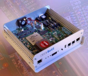
(July 26, 2010) — CEA-Leti developed a digital baseband circuit for software-defined-radio and cognitive-radio applications that features less than 50 microseconds (µs) for full reconfiguration and multi-applications support.Click to Enlarge

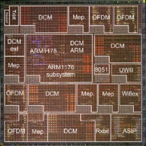
The MAGALI chip, developed for fourth-generation mobile phones, is based on CEA-Leti’s powerful mesh asynchronous network-on-chip (ANOC) infrastructure delivering 2.2GB/s/link. The chip includes 23 integrated processors dedicated to signal processing and bit-level processing associated with an ARM1176 processor for medium access control.

The most powerful innovations have been made on the reconfiguration side. For the first time, a full baseband circuit can be reconfigured in less than 50µs (maximum time), while typical test cases show a 4µs reconfiguration-time (average time observed). Moreover, a multi-application support allows the sharing of the computing units between two radio access technologies (RATs). These two features make MAGALI particularly relevant to software-defined-radio and cognitive-radio applications.

Click to EnlargePower management has been a major optimization goal during the development of this chip. Based on the unique ANOC technology, 23 frequency islands can be programmed dynamically to ensure the best performance-versus-energy ratio. As a result, the circuit exhibits less than 500 mW for up to 40 giga operations per second (GOPS) performance, which is one of the best power efficiency measurements reported for a chip with a high level of flexibility.
MAGALI has been tested on a 3GPP-LTE application, delivering 50Mbits/s on a 4×2 MIMO scheme. It is integrated at present in a prototyping board used in two major European ICT projects, BEFEMTO (www.ict-befemto.eu) and ARTIST4G (https://ict-artist4g.eu/)

CEA-Leti presented the circuit at the flagship 2010 International Solid-State Circuits Conference (ISSCC) earlier this year in San Francisco. Read more about semiconductors at http://www.electroiq.com/index/Semiconductors.html

CEA is a French research and technology public organization, with activities in four main areas: energy, information technologies, healthcare technologies and defence and security. Within CEA, the Laboratory for Electronics & Information Technology (CEA-Leti) is focused on micro and nanotechnologies and their applications. For more information, visit www.leti.fr

Watch video interviews with CEA-Leti researchers from SEMICON West 2010

(July 23, 2010) — In this video interview shot at SEMICON West 2010, Mark Privett, Brewer Science, says that new technologies allow use of higher temperatures as well as room-temperature processes, such as wafer de-bonding. The 3D packaging industry is nearly ready for high-volume, yet still without industry standards.

To see the company’s earlier 2010 interview, recorded at the ConFab with CTO Tony Flaim, click here: http://www.electroiq.com/index/display/semiconductors-article-display/2383506614/articles/solid-state-technology/semiconductors/industry-news/business-news/2010/may/confab-video__end.html

(July 22, 2010) — These market statistics were compiled by Nancy Wu & Mary Olsson, part of the Gary Smith EDA team. The biggest change in 2009 was Mentor passing Cadence to become number two in product sales in EDA. This is an indication of the market shift caused by the move into the ESL Methodology. Synopsys remains a strong number one.

Mentor also grabbed #2 overall in IC design. With the acquisition of Valor, Mentor is also now 3× as large as its next competitor in PCB design.

We believe that the recent changes in Cadence has stopped their market share decline, similar to the changes made at Mentor, bringing in Walden Rhines, during the switch to the RTL design methodology.

Table. Market Share 2009. Note: All numbers show the best estimates of the Gary Smith EDA Analyst. Source: Gary Smith EDA (June 2010)
Rank  2008  2009  Growth, 2008-2009  Market share, 2009
Synopsys 1,227.40   1,250.45   1.9% 31.0%
Mentor Graphics 755.10 758.50   0.5% 18.8%
3   Cadence Design Systems    905.12      746.08   -17.6%  18.5%
Magma Design Automation       159.50      113.80   -28.7% 2.8%
Agilent EEsof       110.10      113.40   3.0% 2.8%
Other  1,074.15 1,051.56   -2.1% 26.1%
All companies 4,231.37   4,033.78   -4.5% 100.0%

Gary Smith EDA Market Statistics are a continuation of the Dataquest EDA Market Statistics that were started in 1985. Gary Smith EDA Market Statistics consist of Market Share, Market Forecast and Market Trends. In order to better serve the start-up community, Gary Smith EDA splits Market Trends into five reports. Basic Service consists or a minimum of one Markey Trend report and ten hours of Inquiry. For more information, visit http://www.garysmitheda.com/contact.php

In this video interview from SEMICON West 2010, Walden Rhines, Mentor Graphics, discusses 3D technologies. EDA tools need to be extended to meet the needs of 3D — parasitic extraction and timing, place-and-route, and other steps are different with 3D. The tools are evolving for various 3D techs.

To watch a video interview with Segare Kekare, Synopsis, about rapid root cause analysis and process change validation using design-centric volume diagnostics, go to: Yield metrology looking at systematic failure mechanisms: Synopsis

by James Montgomery, news editor

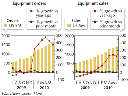
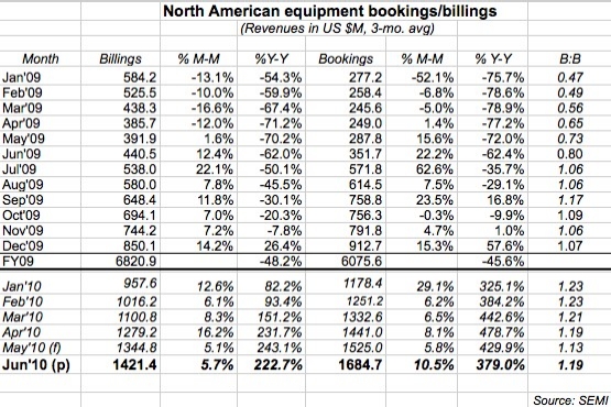
July 22, 2010 – Building on what has become a repetitive, if welcome theme, North America-based chip tool suppliers posted $1.68B in orders in June, up 10.5% from May — officially surpassing their levels before anyone worried about a macroeconomically-induced meltdown. Billings also grew strongly, up 5.7% month/month to $1.42B. (Both metrics still have absurdly high triple-digit Y/Y growth, as much reflective of 2009’s lousiness.) The bigger surge in bookings also pushed the B:B ratio up to 1.19, meaning $119 worth of orders was received for every $100 of product billed during the month.

Click to Enlarge

The numbers "indicate the consistent customer demand that SEMI members are working hard to fulfill," said Stan Myers, president/CEO of SEMI, in a statement.

More inside the June stats:

  • Bookings are at their highest levels since August 2006 (was June 2007), after SEMI once again tacked on an extra bump ($42M) to its previous preliminary monthly tally. The >10% M/M jump in bookings is the biggest since February. Billings are still on a roll, with their highest level since October 2007 (was April 2008).
  • The B:B has stayed above the 1.0 parity mark for 12 consecutive months — the past six of them above 1.13 — indicating that still more business continues to come in (orders) vs. go out (sales).
  • For those tracking the industry’s recovery, here’s the kicker: Bookings are now officially above their peak before the economy-induced crisis ($1641.0M in May 2007), and have risen for 14 out of 15 months (one month was flat). Billings have risen sequentially for 14 straight months. Bookings are closing in on the overall cyclical peak from four summers ago ($1782.3M, June 2006), and billings aren’t far away ($1742.8M, August 2006).


Click to Enlarge

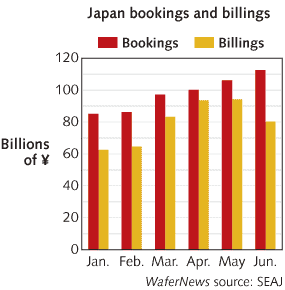
Things in Japan, though, are a bit mixed. Semiconductor equipment bookings rose another 6% in June to ¥112.51B (US $1.29B) — but billings sunk nearly 15% to ¥80.29B ($922.1M), according to the Semiconductor Equipment Association of Japan (SEAJ). That shoved the B:B ratio up to an eye-popping 1.40.

Click to Enlarge

Gartner analyst Bob Johnson, speaking at a market summary at last week’s SEMICON West, offered maybe the best analogy to the industry’s sentiment we’ve heard so far: it’s like we’re approaching the top of a mountain peak, seeing nothing but blue sky and a few clouds ahead and around — and no real visibility as to what’s just on the other side of the peak ahead, be it a plateau or steep dropoff. Anyone want to place a bet?

(July 20, 2010) — Franklin Kalk, Toppan Photomasks, comments on the big EUV lithography news annouced at SEMICON West. Technical challenges of EUV remain defect management — finding and fixing defects in masks. Pattern mask inspection may not be ready until 2016.

More on EUV:
SEMICON West: Lithography trends at Sokudo breakfast forum

Imec and ASML demonstrate potential of 193nm immersion lithography

DUV inspection and defect origin analysis for 22nm spacer self-aligned double-patterning 

(July 20, 2010) — In this video interview from SEMICON West 2010, Walden Rhines, Mentor Graphics, discusses 3D technologies. EDA tools need to be extended to meet the needs of 3D — parasitic extraction and timing, place-and-route, and other steps are different with 3D. The tools are evolving for the various 3D technologies. He also touches on lithography evolution.

Also read:
Workshop addresses simulating, measuring 3D IC stress using TSVs

SEMATECH and Fraunhofer IZFP hosted a follow-up meeting in conjunction with SEMICON West to evaluate a design-for-manufacturing (DFM) approach to managing stress in 3D interconnects, and to drive consensus and support for these techniques across the industry.