Category Archives: Uncategorized

TSMC 20nm Arrives – The First Shoe Drops

By Dick James, Senior Technology Analyst, Chipworks

For us at Chipworks interested in leading edge processes, 2014 so far has been the year of waiting for parts and processes that have been announced, but not shown up in the world of commercial production. It will surprise no-one in the business that they are Intel’s 14-nm, the 20-nm products from any of the big three foundries (in particular TSMC), and vertical NAND (in particular Samsung, since they are the first claiming shipment).

There are of course other products that we are anticipating such as the latest SDRAM, STT or resistive RAM, and anything with TSVs, but they are lower-key and will not get the same attention from the majority of our customers.

So now the first shoe has dropped (must check where that metaphor came from!), and we have a TSMC-fabbed 20-nm part in-house. It is in the lab at the moment, and we are waiting for the analysis results.

It will be interesting to see what changes TSMC has made from the 28-nm process; in general, I expect mostly a shrink of the latter process, with no change to the materials of the high-k stack, though maybe to the sequence. At 28-nm the high- k was put down first, before the dummy poly gate, and it makes sense to move that deposition to after poly gate removal. That way, the high-k layer does not have to suffer the poly formation and source-drain engineering process steps, saving it from quite a bit of thermal processing.

Below is an illustration of a NMOS transistor from a Qualcomm Snapdragon 800, fabricated in the TSMC 28HPM process. The slight indent at the bottom of the metal stack (indicated by the arrow), above the high-k layers, indicates that the high-k was formed before the polysilicon deposition and the subsequent source/drain engineering.

Fig. 1: NMOS Transistor in Qualcomm Snapdragon 800

Fig. 1: NMOS Transistor in Qualcomm Snapdragon 800

The dark line at the perimeter of the metal gate is the tantalum-based barrier layer between the Ti-Al work-function doping layer and the TiAlN work-function layer, and is the first layer formed after the dummy poly removal. Intel used this sequence for their 45-nm process, but modified it at the 32-nm node to deposit the high-k stack after poly removal (high-k last – see below).

Fig. 2 Intel 32-nm NMOS Transistor

Fig. 2 Intel 32-nm NMOS Transistor

You can see that Intel also adopted raised source/drains, with stacking faults to apply tensile stress; we will see if TSMC does the same in their second generation gate-last HKMG process. They could also change the gate fill metal, since in a smaller gate it may be difficult to use the PVD Ti/Al/Cu from the 28nm sequence.

Fig. 3 PMOS Transistor in Qualcomm Snapdragon 800

Fig. 3 PMOS Transistor in Qualcomm Snapdragon 800

When it comes to PMOS, I also expect a high-k last version of the 28-nm gate structure, with the latest version of e-SiGe source/drains, likely with a sigma-cavity etch to the (111) planes. We already have raised source/drains, and the Ge content is ~50%, so not much opportunity for change there.

As for the back-end, presumably there will be a reduction in the k-value of the low-k dielectric, and maybe some thinning of the barrier layer in the metal trenches, both of which are trends that progress relatively slowly by comparison with the front-end.

Back in May, Applied Materials announced a cobalt CVD system aimed at improving copper fill and electro-migration performance. I wouldn’t have expected to see this in use yet, but at Semicon I heard that over 90 of these systems have already been shipped, so there is at least a possibility that we’ll see cobalt in our 20-nm metallization.

All pure speculation, but as a blogger and analyst, I’m paid to speculate!

As for “the first shoe drop”, it’s a variant on “waiting for the other shoe to drop“; apparently it’s a reference to cheap apartment housing where tenants would hear their neighbours above taking off and dropping their first shoes on to the floor; and then wait for the second shoes to drop.

Intel’s e-DRAM Shows Up In The Wild

When Intel launched their Haswell series chips last June, they stated that the high-end systems would have embedded DRAM, as a separate chip in the package; and they gave a paper at the VLSI Technology Symposium [1] that month, and another at IEDM [2].

It took us a while to track down a couple of laptops with the requisite Haswell version, but we did and now we have a few images that show it’s a very different structure from the other e-DRAMs that we’ve seen.

IBM has been using e-DRAM for years, and in all of their products since the 45nm node. They have progressed their trench DRAM technology to the 22nm node [3], though we have yet to see that in production.

Embedded DRAM in IBM Power 7+ (32-nm)

Embedded DRAM in IBM Power 7+ (32-nm) (Click to view full screen)

TSMC and Renesas have also used e-DRAM in the chips they make for the gaming systems, the Microsoft Xbox and the Nintendo Wii. They use a more conventional form of memory stack with polysilicon wine-glass-shaped capacitors. TSMC uses a cell-under-bit stack where the bitline is above the capacitors, and Renesas a cell-over-bit (COB) structure with the bitline below.

Embedded DRAM in Microsoft Xbox GPU fabbed by TSMC (65-nm)

Embedded DRAM in Microsoft Xbox GPU fabbed by TSMC (65-nm) (Click to view full screen)

Intel also uses a COB stack, but they build a MIM capacitor in the metal-dielectric stack using a cavity formed in the lower metal level dielectrics. The part is fabbed in Intel’s 9-metal, 22nm process:

Embedded DRAM in Nintendo Wii U GPU fabbed by Renesas (45nm)

Embedded DRAM in Nintendo Wii U GPU fabbed by Renesas (45nm) (Click to view full screen)

When we zoom in and look at the edge of the capacitor array, we can see that the M2 – M4 stack has been used to form the mould for the capacitors.

General structure of Intel’s 22-nm embedded DRAM part from Haswell package

General structure of Intel’s 22-nm embedded DRAM part from Haswell package (Click to view full screen)

Looking a little closer, we can see the wordline transistors on the tri-gate fin, with passing wordlines at the end of each fin. Two capacitors contact each fin, and the bitline contact is in the centre of the fin.

Intel’s 22-nm embedded DRAM stack

Intel’s 22-nm embedded DRAM stack (Click to view full screen)

We can see some structure in the capacitors, but at the moment we have not done any materials analysis.  A beveled sample lets us view the plan-view:

Plan-view image of the Intel 22-nm embedded DRAM capacitors

Plan-view image of the Intel 22-nm embedded DRAM capacitors (Click to view full screen)

The capacitors are clearly rectangular, but again in the SEM we cannot see any detailed structure. We’ll have to wait for further analysis with the TEM for that!

Intel claims a cell capacitance of more than 13 fF and a cell size of 0.029 sq. microns, so about a third of their 22-nm SRAM cell area of ~0.09 sq. microns, and a little larger than the IBM equivalent of 0.026 sq. microns. The wordline transistors are low-leakage trigate transistors with an enlarged contacted gate pitch of 108 nm (the minimum CGP is 90 nm).

In the Haswell usage the die is used as a 128 MB L4 cache, with a die size of ~79 sq. mm, co-packaged with the CPU.

Intel Haswell CPU with co-packaged eDRAM

Intel Haswell CPU with co-packaged eDRAM (Click to view full screen)

Intel got out of the commodity DRAM business almost thirty years ago; it will be interesting to see where they take their new entry, though not likely into competition with the big three suppliers. Their “Knights Landing” high-performance computing (HPC) platform is reported to use 16 GB of eDRAM, which will take the equivalent of 128 of these chips, so perhaps the future is in HPC and gaming systems such as the one we bought to get the part.

References

[1] R. Brain et al., A 22nm High Performance Embedded DRAM SoC Technology Featuring Tri-gate Transistors and MIMCAP COB, Proc VLSI Symp 2013, pp. 16-17.

[2] Y. Wang et al., Retention Time Optimization for eDRAM in 22nm Tri-Gate CMOS Technology, Proc IEDM 2013, pp. 240-243.

[3] S. Narasimha et al., 22nm High-Performance SOI Technology Featuring Dual-Embedded Stressors, Epi-Plate High-K Deep-Trench Embedded DRAM and Self-Aligned Via 15LM BEOL, Proc. IEDM 2012 pp. 52-55.

IEDM 2013 Preview

Next week, the researchers and practitioners of the electron device world will be gathering in Washington D.C. for the 2013 IEEE International Electron Devices Meeting.  To quote the conference web front page, “IEDM is the flagship conference for nanometer-scale CMOS transistor technology, advanced memory, displays, sensors, MEMS devices, novel quantum and nano-scale devices and phenomenology, optoelectronics, devices for power and energy harvesting, high-speed devices, as well as process technology and device modeling and simulation. The conference scope not only encompasses devices in silicon, compound and organic semiconductors, but also in emerging material systems.”

From my perspective at Chipworks, focused on chips that have made it to production, it’s the conference where companies strut their technology, and post some of the research that may make it into real product in the next few years.

In the last few days I’ve gone through the advance program, and here’s my pick of what I want to try and get to, in more or less chronological order.  As usual there are overlapping sessions with interesting papers in parallel slots, but we’ll take the decision as to which to attend on the conference floor.

For the second year the conference starts on the Saturday afternoon, with a set of six 90-minute tutorials on a range of leading-edge topics:

  • Nano Electronics – The use of Low-Dimensional Systems for Device Applications, Joerg Appenzeller,Purdue University
  • Interface Properties for SiC and GaN MOS Devices, T. Paul Chow, Rensselaer Polytechnic Institute
  • Energy Harvesting for Self-Powered Electronic Systems, Rob van Schaijk R&D Manager Sensors &Energy Harvesters, Holst Centre / IMEC
  • Tunnel FETs – Beating the 60 mV/Decade Limit, Erik Lind, EIT, Lund University
  • Atomic-Scale Modeling and Simulations for Nanoelectronics, Sumeet C. Pandey and Roy Meade,Emerging Memory Group, Process R&D, Micron Technology Inc.
  • 3D Chip Stacking, Mukta Farooq, Systems & Technology Group, IBM

The first three are from 2.45 – 4.15, and the remainder from 4.30 – 6.00.  I won’t make it to any of them; dedicated nerd I may be, but I want at least some of my weekend!

On Sunday December 4th, we start with the short courses, “Challenges of 10nm and 7nm CMOS Technologies” and “Beyond CMOS: Emerging Materials and Devices.

Aaron Thean of IMEC has organised the former, and we have some impressive speakers – Frederic Boeuf, ST Microelectronics, (Device Challenges and Opportunities for 10nm and Below CMOS Nodes), Zsolt Tokei, also of IMEC, (Challenges of 10nm & 7nm Advanced Interconnect), Andy Wei, GLOBALFOUNDRIES, (Process Integration Challenges in 10nm CMOS Technology), Paul Franzon, NCSU, (Manufacturing, Design, and Test of 2.5D- and 3D-Stacked ICs), and Mark Neisser, Sematech (Lithography Challenges and EUV Readiness for 10nm and Beyond). With 14-nm product expected to hit the market next year, we need to look ahead, so this is appropriate  – on the Intel clock, 10-nm is only two – three years away!

I’m now telling folks to think about the end of silicon, at least as we know it, since my brain will not wrap around the idea of 10- and 7-nm gates, and 10-nm gates are only 30 – 40 atoms across, depending on orientation! There’s lots of talk about integrating high-mobility materials onto silicon (imec had an announcement about InGaAs finFETs only a few weeks ago), so this course will help put that into context and cover off how the transistors fit into the rest of the stack.

Tom Theis of SRC has set up the other short course; now that we are reaching the end of silicon transistors, where do we go beyond CMOS?

Ken Uchida of Keio University reprises some of the first course with a session on Extending the FET; then Adrian M. Ionescu from the Ecole Polytechnique Federale de Lausanne discusses Tunnel FETs to give insights into perhaps the best known low-voltage device.

Nanomagnetic Devices are reviewed by Rolf Allenspach from IBM Zurich Research Labs, looking at the material properties and challenges, and some example devices.

All of these futuristic devices have to be compared to each other to see which ones have practical potential, so Dmitri Nikonov of Intel covers off Performance Benchmarking Methodology for Emerging Devices, looking at the rigorous methodology developed by the SRC’s Nanoelectronics Research Initiative, with some comparative results.

The final talk is on Emerging Devices for Quantum Computing by Michelle Simmons from the University of New South Wales, showing the device requirements for a practical quantum computer, then a quick survey of exploratory devices, and a closer look at one or two promising device concepts.

So some good solid stuff – although the courses make a long Sunday, from 9 a.m. to 5.30 p.m., but it’s worth sticking around to the end.

For the first time I can remember the Sunday evening has some extra sessions; Sematech is hosting a session on “Beyond CMOS” at the Fairfax at Embassy Row, from 5:30 – 8:35; and Leti will host a workshop on “Latest Advances in Cost-effective and Power-efficient Technologies for the Future of the Semiconductor Industry” from 6 – 9 pm at the Churchill Hotel, across the street from the Hilton.

Monday morning we have the plenary session, with three pertinent talks on the challenges of contemporary electronics:

  • Graphene Future Emerging Technology, by Andrea Ferrari, from the University of Cambridge – given the developments in this field in the last few years, it’s time to look ahead and try and create a roadmap for this potentially disruptive technology, so this should be illuminating;
  • Heterogeneous 3D Integration – Technology Enabler Toward Future Super-Chips, Mitsumasa Koyanagi, Tohoku University – we are already seeing a form of heterogeneous integration in RF front-end modules (but at the package level), and with Luxtera’s optical interface chips, but this talk will describe the higher levels of integration being researched at Tohoku U and elsewhere.
  • Smart Mobile SoC Driving the Semiconductor Industry: Technology Trend, Challenges and Opportunities, Geoffrey Yeap, Qualcomm. As VP of Technology, Geoffrey Yeap has been at the heart of the mobile revolution, and helped push the company into the top ten; so this should be an interesting review of the last few years of mobile chip developments, and the challenges of squeezing more and more functionality onto ICs, for more and more RF bands, and in ever thinner phones.

At lunchtime ASM is hosting their regular IEDM seminar (Monday this year, instead of the Wednesday as in previous years) on Integrating High Mobility Materials, again at the Churchill Hotel.

After lunch we have seven parallel sessions coming up! Session 2 gets straight into the way-ahead material with papers on germanium & III-V CMOS devices, although we seem to be moving away from R towards D in the R&D spectrum; for example, paper 2.8 from IBM builds InGaAs n- and SiGe p-MOSFETs on hybrid substrates formed by direct wafer bonding of SiGe and InGaAs layers.

Session 3 details MRAM and NAND flash memories, starting with an invited talk by AIST on Future Prospects of MRAM Technologies (3.1), and the session ends with papers from Hynix and Macronix, the former on a 1x-nm multi-level cell NAND flash (3.6), and the latter on a dual-channel 3D NAND flash (3.7).

In session 4, we have the more futuristic topic of Steep Slope Devices, including papers from imec (4.2) and Intel (4.3) on tunnel FETs.

Now that we are into the finFET era, there is an interesting simulation paper in session 5; Analysis of Dopant Diffusion and Defects in Fin Structure (5.7), a joint paper by Panasonic and imec.

Session 6 focuses on Power Devices, with an indication that TSMC is getting into the business; they have a joint paper with Honk Kong UST on interface traps in Al2O3/AlGaN/GaN MIS devices (6.3). Mitsubishi is giving an invited talk on high voltage and large current SiC power devices (6.5), and we get back to MOS with a joint paper on the operating limits of LDMOS from NXP and U Twente.

The first two papers in session 7 discuss the reliability degradation caused by TSVs and 3D stacking, as measured by DRAM retention time; it appears that if wafers are thinned to 30 microns or less the DRAM performance drops off significantly due to stresses caused by the TSVs and microbumps (7.1, 7.2).

This year’s IEDM has focus sessions, and session 8 is the first, on Sensors and Microsystems for Biomedical Applications, with seven invited talks on different aspects of biosensors and biomedical devices.

Then in the evening we have the conference reception at 6:30, through until 8 pm.

Tuesday morning we have another seven parallel sessions, starting with session 9 on Advanced CMOS Technology, so one I will definitely be targeting. The first paper (9.1) is TSMC’s launch of their 16-nm finFET process, with a claimed doubling of logic density over their 28-nm process, with more than 35% speed gain or over 55% power reduction, and a 0.07 sq. micron 6T SRAM cell size.

 Screen Shot 2013-12-06 at 10.28.55 AM

Comparison of TSMC 16-nm finFET performance with 28-nm HKMG planar process (Source: TSMC, IEDM)


That is followed (9.2) by the competing 20-nm FDSOI process from the ISDA Alliance (IBM, STMicroelectronics, Renesas, GLOBALFOUNDRIES, SOITEC, and CEA-LETI).

Paper 9.3 takes us into the world of 3D-IC with a paper on layered ultrathin-body (UTB) circuits stacked on 300nm-thick interlayer dielectric (ILD) layers.


 Screen Shot 2013-12-06 at 10.29.32 AM

TEM image of 3D-layered UTB chip (Source: NNDL/Stanford/NTHU/UC Berkely, IEDM)

Amorphous silicon layers were deposited and crystallized with laser pulses, then planarized with low-temperature CMP to thin the layers, allowing formation of ultrathin, ultraflat devices.

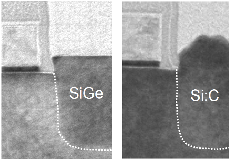
IBM takes the next slot (9.4) with what looks like an update on their 22-nm gate-first process debuted last year (paper 3.3 last year), discussing 2nd Generation Dual-Channel Optimization with cSiGe for 22nm HP Technology and Beyond.

Intel also gives an update, this time on their eDRAM technology disclosed at the VLSI Symposium in June (Retention Time Optimization for eDRAM in 22nm Tri-Gate CMOS Technology, 9.5).

 Screen Shot 2013-12-06 at 10.30.16 AM

Details from Intel eDRAM paper at 2013 VLSI Technology Symposium


The session finishes up with a paper on embedded flash in a 55nm process from Fujitsu (9.6), and one on SRAM-like local interconnect structures for 20nm middle-of-line metallization from GLOBALFOUNDRIES; they claim that this helps them “achieve industry’s most optimum 20nm technology offerings.”

So I guess from the above I will be in session 9 all morning, so I will have to give session 10 on RRAM and FERAM a miss, even though there is interesting progress in the field, including 28nm RRAM in a paper (10.3) co-authored by TSMC.

Session 11 is focused on Flexible Electronics, a look into the future, but not too far away, judging by some of the talks.

Session 12 is the first on Modeling and Simulation, focusing on Technology CAD, with a few topics that catch my eye; paper 12.2 on Alloy Scattering in SiGe Channel from Samsung; Mobility in High-K Metal Gate UTBB-FDSOI Devices, an invited talk (12.5) from STMicroelectronics; Threshold Behavior of the Drift Region: the Missing Piece in LDMOS Modeling (12.7), from NXP; and Copper Through Silicon Via Induced Keep Out Zone for 10nm Node Bulk FinFET CMOS  Technology (12.8), a joint paper from imec and Synopsys.

It seems that session 13 is a bit of a catch-all session on Advanced Manufacturing, since it includes invited papers on 3D memory (13.1) from Micron, GaN-on-Si from Toshiba (13.2), photonics on SOI by Luxtera and STMicroelectronics (13.3), TSMC’s take on glass interposers (13.4) and 450mm (13.7), and III-V growth on 300mm wafers from Aixtron (13.6).

Next we have another bio-session, BioMEMS and BioSensors, including two DNA analysis-on-chip papers (14.1 & 14.3). The last parallel session of the morning is session 15, on Reliability of BEOL and FEOL Devices, and it now seems that graphene and nanotubes have been around long enough that we have an invited talk on their reliability (15.1).

The speaker at the conference lunch will be David Luebke, Senior Director of Research at Nvidia, on the topic, The Current State-of-the-Art and Advances in Visual/GPU Computing.

Session 16 in the afternoon is about III-V Logic, looking ahead to when silicon can no longer provide the performance needed.

Session 17 is another focus session, this time on Analog and Mixed Signal Circuit/Device Interactions. We have a series of invited talks on the impact of nanometer scaling and finFETS on analog design and performance, RF technology, and a look at terahertz RF in CMOS, all of which catch my interest.

We are back to Sensors, Resonators, and Microsystems in session 18, and Nanosheet and Nanotube Technology in session 19, and it seems that molybdenum disulphide is now taking attention away from graphene since there are a couple of papers on that topic.

Session 20 is another multi-topic group of papers, on Fully Depleted Planar, 3D Ge Device Technology and RRAM Memory processing. We have TSMC and GloFo/Samsung/imec talking Ge finFETs (20.1 & 20.4), Si nanowires from IBM (20.2), and gate-last FDSOI from STMicroelectronics and CEA-LETI (20.3); two papers on doping finFETS by AIST/Nissin and AMAT/GloFo/Hynix (20.5 & 20.6); and to finish the session two RRAM talks by Macronix/National TsingHua U and Stanford U (20.7 & 20.8). The last paper uses block copolymer self-assembly lithography to get the device down to less than 12nm.

Memory Characterization and Reliability is the subject of Session 21, mostly of resistive memories; Session 22 is another Modeling and Simulation group of papers, this time on Innovative Devices, mainly resistive memories.

That brings us to the end of the afternoon, and now we have a dilemma – three offsite events – IEDM is getting popular with the industry! Applied Materials is hosting a panel on “3D NAND Is a Reality – What’s Next?” at the Omni Shoreham Hotel from 5 – 7.30 pm; Coventor is also hosting a panel at the Churchill Hotel, from 5:30 – 8:30, on “Insights from the Experts on Advanced Technology Development”; and Synopsys is having a TCAD reception, again at the Churchill, from 6 – 8 pm.

Once we’re sated from the hospitality, we can wander back to the Hilton and try and stay awake for the conference evening panels:

“Is there life beyond conventional CMOS?” moderated by Jeff Welser of IBM – now becoming a perennial question! The panelists are An Chen (GLOBALFOUNDRIES), Tetsuo Endoh (Tohoku University), Marc Heyns (IMEC Fellow), Mark Rodwell (UC Santa Barbara), Alan Seabaugh (Notre Dame), and Ian Young (Intel).

And:

“Will Voltage Scaling in CMOS Technology Come to an END?” with Kevin Zhang of Intel as moderator. Panelists for this session are Rob Aitken (ARM), Kelin Kuhn (Intel), Sreedhar Natarajan (TSMC), Tak Ning (IBM), Ann Steegen (imec), and Nobuyuki Sugii ( LEAP).

Wednesday morning has sessions 25 – 30; S25 on Advanced 3D Packaging and Emerging Memory Systems; TSMC is detailing an Array Antenna Integrated Fan-out Wafer Level Packaging (25.1), and Maxim is giving an invited talk on 3D Heterogeneous Integration for Analog, as the first two papers.

S26 covers Ge Channel and Nanowire Devices, obviously looking ahead, but catching my interest are A Group IV Solution for 7nm FinFET CMOS (26.3), from Synopsys/Stanford, and A Practical Si Nanowire Technology… (26.5) from Samsung.

Session 27 – Display and Imaging Devices has three papers on thin-film transistors for displays, and three imaging talks; Sony describes a Three-dimensional .. 1.20 μm Pixel Back-Illuminated CMOS Image Sensor (27.4), and Infineon has a novel Trench Gate Photo Cell (27.6) which could find use as the ambient light sensor that we see in so many mobile phones.

We have more III-V and TFET papers in session 28, but including an invited talk from Raydeon (More than Moore: III-V Devices and Si CMOS Get It Together – 28.5) on integrating III-V devices with Si CMOS on a common silicon substrate, which should be interesting in these days of 3D.

Session 29 has a couple of interesting papers on BEOL from Renesas and Samsung (29.1 & 29.2), and Hitachi/ASET discusses Fabricating 3D Integrated CMOS Devices by Using Wafer Stacking and Via-last TSV Technologies (29.5).

Conductive Bridge and Phase Change RAM papers make up session 30; the first two are CBRAM, and the rest PCM. Micron discusses Interface Engineering for Thermal Disturb Immune Phase Change Memory Technology in paper 30.4.

After the morning sessions, the IEDM Entrepreneurs Lunch is back for a second year, with Steve Nasiri, founder of Invensense, and now angel investor and mentor at Nasiri Ventures LLC, as guest speaker.

We are back to Characterization, Reliability, and Yield in S31 after lunch, with a focus on Device Variation and Noise. STMicroelectronics is giving an invited presentation on the Growing Impact of Atmospheric Radiations on sub-65nm CMOS BULK/FDSOI Technologies (31.1), we have two papers on SRAM, and the last three discuss random telegraph noise in MOSFETs, resistive RAM, and HEMTs, respectively.

Session 32 is the third Modeling and Simulation session, this time on Modeling Beyond CMOS Devices, Interconnects and GaN HEMT – getting a bit esoteric for my focus, unfortunately – but then with all the parallel sessions we have to miss some of them.

The last session (numerically), session 33, covers Circuit/Device Variability and Reliability. Asen Asenov of University of Glasgow/Gold Standard Simulations has a joint paper with IBM on Simulation Based Transistor-SRAM Co-Design in the Presence of Statistical Variability and Reliability (33.1), detailing the impact of process and statistical variability and reliability on SRAM cell design in 14nm technology node SOI FinFET transistors; with Intel’s 14nm due next year we might get some insights, though time will tell if they have moved to SOI trigate transistors from the bulk material that they currently use at 22nm.

By the end, I’m usually suffering from information overload and becoming brain-numb, but with 215 papers and an average of six parallel sessions at any one time, plus the offsite events, that’s not really surprising. On the other hand, where else do we go to get all this amazing stuff?

GLOBALFOUNDRIES to make Apple chips in New York fab?

I normally don’t have the time to follow local press, but occasionally Google Alerts pops up with something quite interesting. In this case, the Albany Times Union from Albany, New York had an intriguing headline that supports some of the gossip around Apple’s fabrication plans for their A-series processor chips, up to now fabbed by Samsung.

At least in the short term, and from a technology point of view, this makes a lot more sense than Apple’s much-vaunted switch to TSMC, since GLOBALFOUNDRIES (as part of the Common Platform alliance with Samsung) uses a gate-first HKMG process rather than TSMC’s gate-last strategy. In fact, a couple of years ago GLOBALFOUNDRIES and Samsung announced that they were synchronizing their fabs so that customers could transfer products from one foundry to the other without the pain of redesign.

At the 20-nm node it might be different story, since all the foundries will be using gate-last processes; I can see TSMC picking up some of the business then, and there are persistent rumours of Apple trial lots going through TSMC.

It also makes sense that GLOBALFOUNDRIES would make a pitch for the Apple work, since they are hungry for customers, and if they can get in at the 28-nm node they will be well positioned for 20-nm products in the next A-chip generations. Apple business would also help fill the potential second fab for which they have obtained outline planning permission in the Luther Forest Technology Campus.

When it comes to the processes, the 28-nm samples that we have seen from GloFo and Samsung are remarkably similar; this is a SEM cross-section of the transistors and first-level metal in the Rockchip RK3188 that Ajit Manocha announced at Semicon West:

Rockchip RK3188_branded 1
Now let’s look at a similar section out of a Samsung Exynos 5410 app’s processor:

Samsung Exynos 5410_branded 2

There may be some very subtle differences that show up in very detailed analysis, but essentially they look pretty close; the fab synchronizing looks good to me!

So the Times Union report may be just a blog rumour, but given the apparent compatibility of the two processes, it has the whiff of authenticity, and we may see A7s out of New York State in the not too distant future.

Now, if we get one into Chipworks, can we tell the difference?

Apple A7 uses Samsung’s 28nm process

Last week, we started tearing down the Apple iPhone 5S. There has been much speculation that Apple would be moving their processor chips over to TSMC, but I think that we can now decisively say that this has not occurred – they have migrated to 28nm, but still at Samsung.

Apple's A7 Processor Die Image (click to view full screen.)

Apple’s A7 Processor Die Image (click to view full screen.)

Earlier in the day last Friday we established from the look of the die that the A7 was manufactured by Samsung. In the meantime our guys have been grafting away in the lab, and came to the “boring” conclusion that the chip looked exactly the same as the last one.

The devil is in the details, however, and we have to do some measurements to see the difference.

Below is a SEM image of a cross-section of a group of transistors in the A6 (APL0598) chip, fabbed in the Samsung 32nm high-k-metal gate (HKMG) process.  For convenience we have measured ten, so the dimension of the contacted gate pitch is 123nm.

SEM Cross-Section of Apple A6 (APL0598) Die (click to view full screen)

SEM Cross-Section of Apple A6 (APL0598) Die (click to view full screen)

Now if we look at a similar image of the A7 (APL0698) below, and we see that the contacted gate pitch is 114nm. So, even allowing for measurement error (we figure +/- 5%), we’re pretty sure that we see a shrink, and that the A7 is made on the same process as the new Samsung Exynos 5410, the 28nm HKMG process.

SEM Cross-Section of Apple A7 (APL0698) Die (click to view full screen.)

SEM Cross-Section of Apple A7 (APL0698) Die (click to view full screen.)

That doesn’t sound much, a mere 4 nm, but again if you do the math and remember  that we’re talking area shrink, not linear dimensions, then 28^2 divided by 32^2 (784/1024) comes out at about 77 percent of the area for the equivalent functionality. Or, given that the A7 is 102 mm^2 compared with 97 mm^2 for the A6, more functions in a slightly bigger area.

Below is a delayered sample of the A7, but we have yet to identify what that functionality is, something that we will be doing in the next few weeks.

Transistor-Level Image of the Apple A7 (click to view full screen)

Transistor-Level Image of the Apple A7 (click to view full screen)


Qualcomm Snapdragon 800 and Rockchip RK3188 – Battle of the Foundries!

The Snapdragon 800 (Qualcomm MSM8974) is Qualcomm’s leading-edge, low-power, mobile phone app’s processor with built-in 3G/4G LTE modem, using the latest Krait 400 CPU rated at 2.3 GHz and their 450 MHz Adreno 330 GPU. It was launched at this year’s CES International with this rather slick commercial.

Significantly, it is fabricated using the TSMC 28HPM (28-nm, High-Performance Mobile) process, which extends TSMC’s high-k, metal gate (HKMG) processing into the mobile space. Before this, all Qualcomm’s mobile chips were made with the TSMC 28LP polysilicon gate/SiON process; and to our knowledge, this is the first volume production part using 28HPM.

The 28HPM process sees a shrink in minimum gate lengths and SRAM cell size when compared with the 28HP process, and the inclusion of embedded SiGe source/drains for PMOS strain, which was not part of 28HPL.


TSMC 28HPM PMOS transistor

TSMC claims the technology can provide better speed than 28HP while giving similar leakage power to 28LP. The wide performance/leakage coverage apparently makes 28HPM ideal for applications from networking, tablet, to mobile consumer products.


The Rockchip RK3188 is targeted on tablets rather than phones, but it uses the GLOBALFOUNDRIES’ 28SLP (Super Low Power) process, their equivalent to TSMC’s 28HPM, aimed at mobile products. It is again a quad-core part, this time with ARM A9 CPUs running at 1.6 GHz, and quad-core ARM Mali GPUs rated at 600 MHz.


Rockchip RK3188 floorplan showing some of the major functional blocks

Rockchip has squeezed the functionality into ~25 sq. mm, less than a quarter of the size of the Qualcomm chip; not least because the A9 cores are noticeably smaller than the Qualcomm-designed Krait cores based on the ARM architecture, and of course there is no LTE.

GLOBALFOUNDRIES is obviously happy to have won the Rockchip business – their CEO Ajit Manocha specifically mentioned the partnership in his keynote talk at Semicon West:


The 28SLP process differs in a basic way from the TSMC 28HPM – GloFo is using their version of the Common Platform (GLOBALFOUNDRIES, IBM, Samsung) 28-nm process, which is a ‘gate first’ variety, i.e. a polysilicon gate is used with a HKMG stack at its base, doped to form NMOS and PMOS transistors. TSMC’s ‘gate last’ process uses a sacrificial polysilicon gate for all the processing up to the end of the source/drain processing, then the polysilicon is removed and replaced with distinct HKMG stacks which are tuned for NMOS and PMOS.

Like the other Common Platform HKMG processes, a SiGe channel is used in the PMOS transistors, though with GloFo’s own spin – none of these processes are the same from the different vendors.

Compared with the older 32-nm HKMG process used for AMD processors, the Rockchip uses bulk silicon, not SOI, and gate lengths, contacted gate pitches and SRAM cell size are shrunk, but in the same ballpark as TSMC’s process. There is no dual-stress liner or embedded SiGe source/drains to enhance PMOS performance, but this product is rated at 1.8GHz rather than TSMC/Qualcomm’s 2.3 GHz.


GLOBALFOUNDRIES 28SLP PMOS transistor

So we have two processes targeted at similar spaces, but with very different takes on how to do it. TSMC and Qualcomm are following the industry norm, supplying chips to a US company from Taiwan, and GLOBALFOUNDRIES and Rockchip have reversed the trend, supplying chips to China from the West, and it’s tempting to speculate they are from the Malta fab in New York.

A Dispatch from SEMICON West – Applied Materials Launches Epi System Focused on NMOS Strain

Flying in to SFO on July 7, I must have been one of many attendees delayed by the after-effects of the Asiana Airlines crash there the day before. In my case it was only an hour or so (i.e. as normal), but we couldn’t avoid seeing the remains of the aircraft as we landed. Despite the fact that the plane was burnt out, I couldn’t help being impressed that the main body of the plane had survived the impact, and of course all but two of the passengers survived – and they were outside the plane.

By coincidence I flew through Heathrow a week after another 777 did a belly-flop there a few years ago, and again I was impressed at the strength of the airframe – an engine had been ripped off a wing but otherwise it was pretty well intact – and fortunately in that case there was no fire, and no fatalities.

That’s hardly relevant to SEMICON West of course, but it’s hard not to get involved when we get that close to the statistics of travel accidents, be they road, rail or air.

Anyway – back to the show – or at least the pre-show events. Applied Materials (AMAT) had an analyst day on Monday, and in the morning they invited a few of us to some product launches. The one that caught my eye and ear was a new epi system focused on NMOS epitaxial source/drains to create channel strain, since that has been mooted as a next step for several years now, but not shown up in a production context.

The theory is that if you can get carbon and phosphorus to replace silicon atoms in the crystalline structure, because they are smaller than silicon, they will generate tensile stress in the crystal lattice. When it is deposited in cavities etched in source/drains the stress is applied to the channel. (Putting the larger germanium atoms in the lattice has the opposite effect, and creates compressive stress, an effect used since the 90nm node.)


Schematic of e-SiGe in PMOS (left), and e-Si:CP in NMOS (right) source/drains

The problem (as I understand it) has been that the carbon does not like staying in such substitutional positions, and it will abandon them as soon as it sees anneal temperatures, thus losing the stress effect. Phosphorus is happy to be substitutional, and has of course been used as a n-type dopant for decades, so I suspect the problem there is simply getting the concentration to a level sufficient to stress the lattice.

So on Monday AMAT launched the Applied Centura RP Epi system with an NMOS transistor application. To quote: “This capability supports the industry’s move to extend epi deposition from PMOS transistors to NMOS transistors at the 20nm node, enabling chipmakers to build faster devices and deliver next-generation mobile computing power.”


The Applied folks seem confident that once the epi is formed, the carbon can be kept stable and capable of applying the strain at the end of the manufacturing process. I quizzed them as to how this is done and apparently the keys are the quality of the clean after cavity etch (i.e. AMAT’s Siconi dry clean), plus millisecond annealing to minimize the thermal budget.

There is plenty of literature documenting the effect; at last year’s IEDM conference, IBM announced their 22nm server process, which uses embedded strain for both N- and P-MOS[1]. Together with nitride stress, they claim a 10 percent performance increase over the 32nm equivalent. I also asked the speaker there about the carbon stability, and he confirmed that they regard it as a manufacturable process.

Cross-section of NFET showing embedded Si:C Source/Drain Stressor [1]

It seems the time of e-Si:CP NMOS is here. Applied certainly hopes so: they estimate the available market at over $500M and expanding, and that revenue has doubled over the last five years, and they have more than 80 percent share. They see an incremental $250M in revenue from epi systems by 2016.

I’ve been waiting for epi-strained NMOS for the last couple of process generations, and had almost been convinced that it wouldn’t happen. Now we have to watch for it when we get the next 20nm parts!

[1] S. Narasimha et al., “22nm High-Performance SOI Technology Featuring Dual-Embedded Stressors, Epi- Plate High-K Deep-Trench Embedded DRAM and Self-Aligned Via 15LM BEOL”, IEDM 2012, pp 52 – 55.

Economy Threatens Semi Growth, not Technology – so Say Fab Engineers at ASMC

It’s still spring in the north-eastern part of North America, and that means it’s the time of year for the Advanced Semiconductor Manufacturing Conference, in the amiable ambiance of Saratoga Springs, New York. The conference took place last month, on May 13 – 16.

As the name says, ASMC is an annual conference focused on the manufacturing of semiconductor devices; in this it differs from other conferences, since the emphasis is on what goes on in the wafer fab, not the R&D labs, and the papers are not research papers. After all, it’s the nitty-gritty of manufacturing in the fab that gets the chips out of the door, and this meeting discusses the work that pushes the yield and volumes up and keeps them there.

I always come away impressed by the quality of the engineering involved; not being a fab person myself any more, it’s easy to get disconnected from the density of effort required to equip a fab, keep it running and bring new products/processes into production. Usually the guys in the fab only get publicity if something goes wrong!

There were 81 papers spread over the three days, with keynotes from Subi Kengeri of GLOBALFOUNDRIES, Vivek Singh and Tim Hendry of Intel, and Bill McClean of IC Insights, and also a panel discussion on the benefits/pitfalls of 450mm wafers. This latter is particularly apposite here in Saratoga Springs since we have the Global 450 Consortium building their new fab at CNSE in Albany, just down the road from here.

The conference kicked off with Subi Kengeri’s keynote – “Assessing the Threats to Semiconductor Growth: Technology Limitations versus Economic Realities” – essentially, will Moore’s law run out of steam before or after chips get too expensive to sell?
??????

Subi Kengeri of GLOBALFDOUNDRIES giving the opening keynote at ASMC

On the one hand, we anticipate huge growth in revenue on the back of the mobile industry, with the foundries expected to outpace the overall industry, and leading-edge revenue doubling in the next five years:

And we know that technologically we can get to 14nm or even 10nm with multiple patterning, finFETs, etc., and possibly new materials.

On the other hand, SoC designs are getting larger, faster, and more complex, and wafer fab costs are going up, with lithography being the biggest component. (It’s worth noting here that at the 20nm generation, the middle-of line (MOL) processing separates from the back-end of line (BEOL), since the 1X interconnect level has to be double-patterned.)

This increased design and fab complexity also adds to development time and increases the time-to-volume (TTV), adding a time cost and reducing the return on investment.  This could conceivably get the industry into a feedback loop, since TTV delay slows down industry growth, which slows downs investment, which slows down development, which slows down TTV.

The other obvious effect is the industry consolidation which we’ve all been part of – according to Subi only four companies will be fabbing at the 14nm node:

I had wondered why IBM wasn’t on the list until I saw the 50K wafers/month cut-off; even with all the games chips that IBM has churned out over the last few years, I doubt that IBM has hit that number.

If the predictions are correct, by 2016 28nm and below will make up 60 percent of the foundry market, split between four companies (or three, if Intel’s foundry ambitions don’t work out). That thought raised the prospect of capacity limitations, and gave Subi a chance to promote GLOBALFOUNDRIES as the only one of the three with a global footprint, and not in geographically or politically risky zones. 

He finished his talk by identifying critical growth enablers for the industry as optimized SoC technology architecture (with a focus on techno-economics), coupled with true collaborative R&D, and of course the global footprint. And he also asked all of us in the room which was the biggest threat to growth – technology scaling limits, or the economic realities? Being techies, we all know that the next few generations are within sight technically, so we all voted for the economic problems – the part we can’t control!
???

The final vote

As you can see, the vote was pretty overwhelming.

N.B.  All images courtesy of GLOBALFOUNDRIES.

Intel Foundries MEMS for Fuel Cell Start-up Nectar

In the last couple of years there have been announcements that Intel will be acting as a foundry for FPGA company Achronix, PLD maker Tabula and programmable network processor provider Netronome, as well as much speculation about making chips for Apple.

All these reports refer to using Intel’s leading-edge 22-nm tri-gate process. However, at CES a couple of weeks ago, my eye was caught by a 200-mm wafer on display at the booth of a little company called Nectar, who were pitching their fuel-cell based USB charging system. They claim that the charger can top up an iPhone battery at least ten times before the fuel pod has to be changed. The whole device can be held in one hand:


Fig. 1 Nectar fuel-cell charger (at right) on display at CES
The cell uses butane fuel in a silicon-based power cell, and by the look of the image below the cells are ~22 mm square.

Fig. 2 Nectar MEMS wafer on display at CES

The press pack given out at the show includes a paper [1] with a description of the technology; a solid oxide fuel cell (SOFC) is used, which is compatible with silicon processing. I’m not a fuel cell expert, so to quote from the paper:

"Fuel cells operate by creating opposing gradients of chemical concentration and electrical potential. When an ion diffuses due to the concentration gradient, the associated charges are transported against the electric field, generating electrical power. In the case of SOFCs, the mobile ion is O2-, and the oxygen gradient is created by providing air on one side (the cathode) and a fuel mixture which consumes any free oxygen on the other side (the anode). Any fuel which burns oxygen will produce power in an SOFC." The schematic below (Fig. 3) illustrates the process.


Fig. 3 Operating principle of solid oxide fuel cell

The butane has to be cracked so that hydrogen is available, which is done in a "fuel processor" within the cell. The following diagram shows the sequence of power generation [1].


Fig. 4 Diagram of fuel cell power generator

The Nectar generator chip contains the fuel processor, fuel cell stack, and catalytic converter. The fuel processor cracks the butane into hydrogen and carbon monoxide by using a lean mixture of air and butane to give incomplete combustion; then O2- ions from the air feed on the other side of the SOFC stack migrate through the stack and combine to give water and carbon dioxide; then the exhaust gases exit through a catalytic converter.

It is here that the MEMS structure comes in – even incomplete combustion of the butane gives temperatures of 600 – 800C, so to integrate this into a package that can be carried around, and also must have conventional silicon for power conditioning has to be a challenge. The fuel processor uses a mechanically suspended reaction zone formed in silicon, with a heat exchanger adjacent to the reaction zone, as shown in Fig. 5 [1, 2]:


Fig. 5 Experimental (top) and later (bottom) MEMS fuel processor

The nitride tubes contain the gas stream, while the silicon bars provide the heat transfer from the exit stream to the input stream. Fig. 6 shows the modeled heat transfer in a pair of tubes (red = hot, blue = cool) [1]. The U-bend at the end is the reaction zone; ignition is started using a platinum heater deposited on the surface, and once started continues autothermally.


Fig. 6 Schematic of modeled heat recovery in reaction loop

The SOFC itself is built of yttrium-stabilized zirconium oxide (YSZ) plates held in a nitride matrix, supported on silicon walls. In order to keep the profile as slim as possible a "planar stack" of plates is formed as shown schematically in Fig. 7(a), with the detail of a single plate in Fig 7(b)[1].


Fig. 7 (a) Schematic of SOFC plates and (b) Cross-section of single cell

Details of the anode and cathode materials are not given, but they clearly have to be porous to allow the gases to diffuse through and react. Similarly nothing is said about the catalytic converter, but that also should be compatible with MEMS manufacturing.

The inherent ability of MEMS processes to provide vacuum-sealed structures helps contain the heat generated within the system, and the chamber is lined with reflective shielding to further reduce heat losses. Even so a new sealing glass had to be developed, since the conventional lead-glass frits used in many MEMS devices was not up to the job.

The whole assembly is packaged in a “tin can” with the gas inlets and exits on the reverse side of the package:


Fig. 8 Assembled and packaged Nectar fuel cell

Of course, smart as the fuel cell manufacturing is, it is only part of a charging system. Fig 9 [1] is a block diagram of the whole system, showing the peripheral components needed to complete the unit and turn it from a concept into a functioning charger. The battery allows power to be drawn instantaneously from the charger while the fuel cell fires up, and also powers the supporting components. 

Fig. 9 Block diagram of Nectar fuel-cell charging system

I started this blog off by talking about Intel, then veered off into a description of the Nectar charger – what was I babbling about? Well, when I was looking at the charger at CES I had a word with Sam Schaevitz of Lilliputian Systems, which developed the Nectar, and asked him who made the MEMS, expecting to hear about of one of the MEMS foundries that are around. (Lilliputian is a spin-off of MIT – Sam is founder and CTO.)

Much to my surprise, he answered "Intel"! As I said at the beginning, there has been quite a bit of comment about Intel moving to the foundry model, but nothing about them being in the MEMS business. It turns out that the work is done at Intel’s fab in Hudson, Mass., which those with long memories will recall was the DEC fab bought by Intel when DEC went under back in 1998.

I had assumed that it would have been closed long ago, but Intel claims to have put $2B into the plant, converting it to 130 nm back in 2001, and it’s now known as Fab 17. It is now Intel’s sole remaining 200 mm facility. In addition they have their Massachusetts Microprocessor Design Center and the Massachusetts Validation Center on the same site, employing ~1700 in total.


Fig. 10 Intel’s Fab 17 in Hudson, MA (source: Intel)

Intel’s Global Manufacturing Fact Sheet states that the fab manufactures “chipsets and other” – the Nectar chip is clearly an “other”! Nectar announced their supply link with Intel back at the end of 2010, but I missed it at the time; Intel Capital also has a stake in Lilliputian.

Aside from the regular processing equipment, Intel must have invested in deep RIE etchers, never mind the deposition gear capable of forming YSZ and the other exotic materials likely used for the anode/cathode and catalytic converter. Presumably Intel’s need for 130-nm chipsets is slowly fading; this looks like a praiseworthy way of keeping the fab going, as well as supporting a local start-up – and one wonders what other foundry work is going on there. If you do have the urge to buy a Nectar mobile power system, it will be available through Brookstone in the summer.

References:

[1] S. Schaevitz, Powering the wireless world with MEMS, Proc. SPIE 8248, Micromachining and Microfabrication Process Technology XVII, 824802 (February 9, 2012)

[2] L. Arana et al., A Microfabricated Suspended-Tube Chemical Reactor for Thermally Efficient Fuel Processing, J. MEMS 12(5) 600-612

IBM surprises with 22nm details at IEDM

Monday afternoon at the 2012 IEEE International Electron Devices Meeting, IBM discussed their 22nm SOI high-performance technology [1], aimed at servers and high-end SoC products. To an extent, this is an extension of the 32nm process, using epitaxial SiGe for the PMOS channels and stress, and dual-stress liners for both NMOS and PMOS strain. However, there were a couple of surprises buried in there — at least for me!

The first surprise was that this is a gate-first process, contrary to the announcements made by the Common Platform group that the 20nm class processes would be gate-last. The difference seems to be that this technology IS aimed at high performance servers and their support devices, not consumer products, and this is IBM’s process for its high-end products, so they are sticking with the proven formula and pushing it to the next level.

The gate dielectric stack has been scaled to reduce the inversion thickness (tinv) by 7%/10% (NMOS/PMOS), without affecting mobility, modifying the clean, depositions (using ALD for the interfacial oxide), and anneal steps to achieve the lowest tinv published so far, and reducing DIBL by 6%/8%.

The second surprise was that e-Si:C (embedded carbon-doped source/drains) has been used for NMOS stress — IBM claimed that this is the first time in a production process. I had just about written e-Si:C off as a viable manufacturing technique, since I’ve been hearing over the last few years that the carbon is not stable and does not stay in the substitutional crystalline sites where it’s needed. However, here we are told that it is stable and that it survives all the backend processing, even with the 15 layers of metal used in this technology.

Fig. 1: TEM cross-sections of e-SiGe in PFET (left), and e-Si:C in NFET [1]

The e-Si:C incorporates ~1.5% C, which combined with fourth-generation e-SiGe with more Ge and the dual-nitride stress liners, gives 25% more strain than the 32nm process.

The gate-first approach allows conventional contacts and self-aligned silicide, and judging by Fig. 3, raised source/drains help to reduce S/D resistance and keep the gate/contact capacitance under control.

The embedded trench DRAM is not a surprise, IBM has a long history in the field and they have now brought it to the point where access time is shorter than SRAM [2, 3, 4].

Fig. 2: IBM roadmap for e-DRAM [2]

The big change here is that the substrate wafer has an N+ epi layer on it to replace the diffused cell plate of earlier generations. This allows denser packing, since a formerly-needed diffused spacer is removed, giving a cell size of 0.026 μm2. It also enables deeper trenches, giving higher cell capacitance for an areal capacitance of 280 fF/ μm2. The trench capacitors are also used as decoupling capacitors, and these are isolated by deep trench isolation so that they can be biased independently.

Fig. 3: (left) SEM cross-section of e-DRAM trench capacitors; (right) plan-view and
cross-section schematics of decoupling and isolation trenches, showing N+ epi plate
[1]

(As an aside, one of the comments from Greg Taylor of Intel in his microprocessor talk in Sunday’s IEDM short course was that the analog functions that are part of a CPU are getting more significant as dimensions shrink. Both Intel and IBM are now using on-chip decoupling capacitors; Intel with MIMCAPs, and IBM with trench capacitors.)

The complexity of IBM’s server chips is reflected in the 15 levels of metal. The first level is doubled-masked with a litho-litho-etch sequence to allow for orthogonal layout; the rest are single-patterned using uni-directional layout. Self-aligned vias help with packing, and both ultralow-k and low-k dielectrics are used as needed.

IBM is prototyping 22nm server parts right now, but even when they get into the servers for sale, I likely won’t get my hands on one — a bit beyond my procurement budget!

[1] S. Narasimha, IEDM 2012 pp. 52-55
[2] S. Iyer, ASMC 2012
[3] N. Butt, et al., IEDM 2010 pp. 616-619
[4] J.Bart et al, IEEE Journal of Solid-State Circuit, Jan 2011