Author Archives: insights-from-leading-edge

IFTLE 122: TSMC officially ready for 2.5D, Apple order impact on TSMC

An event that many of us have been waiting for, for a long time finally happened a few weeks ago. At the recent TSMC Open Innovation Platform Ecosystem Forum on October 16th, TSMC announced the foundry reference flow supporting CoWoS (Chip-on-Wafer-on-Substrate) within their open innovation platform (OIP) [link].

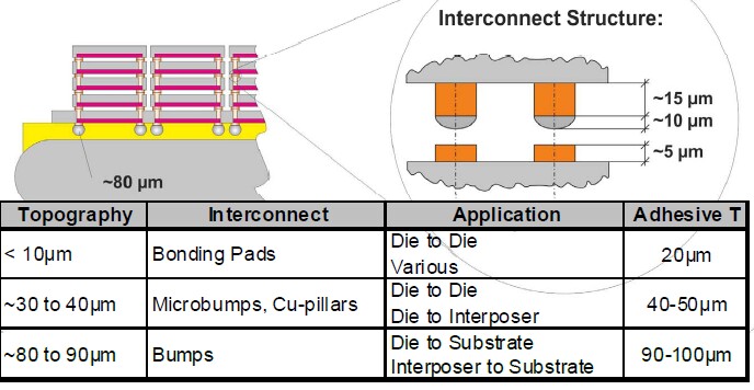
The validated CoWoS reference flow enables "multi-die integration to support high bandwidth, low power and achieve fast time–to-market for 3D IC designs." The CoWoS flow allows designers to use existing, mainstream tools from leading EDA vendors. It reportedly allows "a smooth transition to 3D IC with minimal changes in existing methodologies." It includes the management of placement and routing of bumps, pads, interconnections, and C4 bumps; innovative combo-bump structure; accurate extraction and signal integrity analysis of high-speed interconnects between dies; thermal analysis from chip to package to system; and an integrated 3D testing methodology for die-level and stacking-level tests.

TSMC also announced that they have taped out the foundry segment’s first CoWoS test vehicle using JEDEC Wide I/O mobile DRAM interface [link]. This test vehicle demonstrates the integration of a logic SoC chip and DRAM into a single module using the Wide I/O interface. Along with Wide I/O mobile DRAM, the integrated chips provide optimized system performance and a smaller form factor with significantly improved die-to-die connectivity bandwidth. Ecosystem partners included: Wide I/O DRAM from Hynix; Wide I/O mobile DRAM IP from Cadence Design Systems; and EDA tools from Cadence and Mentor Graphics.

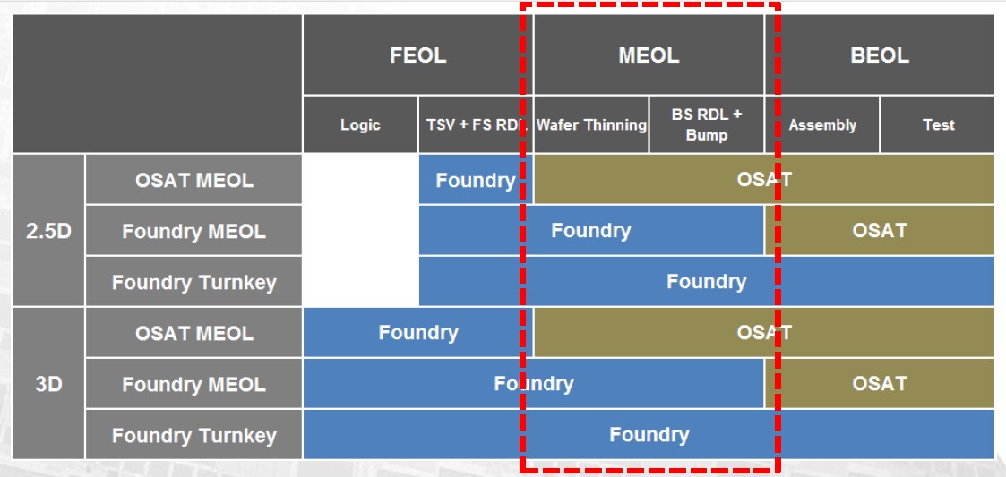
EDA systems in place

It seems like only yesterday there were no EDA tools for 2.5/3DIC [ see PFTLE 23, IMEC arrives in Hsinchu and other 3D IC News]. IFTLE is happy to announce that that is no longer the case with several EDA companies including Cadence, Mentor, Synopsys and Ansys were announced by TSMC as partners for their CoWoS reference flow.


[Cliff Hou, VP R&D TSMC, and CP Hsu, VP R&D Cadence]

Cadence announced that TSMC has validated Cadence 3D-IC technology for its CoWoS reference flow with the development of a CoWoS test vehicle that includes an SoC with Cadence Wide I/O memory controller and PHY IP [link]. This is the foundry segment’s first silicon-validated reference flow enabling multiple die integration.

The validated technologies in the 3D-IC solution include: the Cadence Encounter RTL-to-signoff and Virtuoso custom/analog platforms; the Cadence system-in-package products, and recently acquired Sigrity power-aware chip/package/board signal integrity solution that helps

engineers overcome die-stacking and silicon carriers’ challenges from planning through implementation, test, analysis and verification. TSMC’s unique CoWoS combo bump cells, which simplify bump assignment, are now supported automatically in the Cadence Encounter Digital Implementation (EDI) System, QRC Extraction, and Cadence Physical Verification System. The CoWoS Reference Flow is supported with a CoWoS design kit and silicon validation results from a TSMC test vehicle.

Mentor Graphics announced IC physical design, verification, thermal analysis and test design tools that have been selected for TSMC’s new CoWoS (Chip on Wafer on Substrate) Reference Flow [link].

The Olympus-SoC product supports "probe pad routing including micro bump and C4 bump routing, routing between combo bumps, and combo bump stream out in DEF and GDS formats. Inter-die design rule checks (DRC) and layout versus schematic (LVS) checks are performed during layout construction to help ensure rapid signoff."

The Pyxis IC Station custom layout product "provides redistribution layer (RDL) routing and ground plane generation with the ability to do 45 degree angle routes to vias, and specific enhancements for the TSMC flow include improvements to the bump file import process".

The Calibre 3DSTACK sign-off tool verifies physical offset, rotation, and scaling at the die interfaces. It can also trace connectivity and extract interface parasitics to enable multi-die performance simulation. Calibre and FloTHERM 3D computational fluid dynamics software have been integrated to model temperature variation across the CoWoS design.

The Tessent solution enables 3D IC testing. The Tessent test tool " addresses 3D IC multi-die integration challenges including management of placement and routing of micro-bumps, probe-pads, through-silicon-vias (TSVs), and C4 bumps, accurate extraction and signal integrity analysis of high-speed interconnects between dies, thermal analysis from chip to package to system, and integrated 3D testing methodology for die-level and stacking-level tests".

Key features for 3D IC include:

  • Pre-bond testing of TSVs and IOs using contactless wrap;
  • Retargeting of embedded compression scan patterns and built-in self-test (BIST) created at the die level to any die in the stack using DFT access infrastructure;
  • Test generation for shorts or opens between logic die;
  • Test generation for shorts or opens between DRAM and logic die using the memory die’s JEDEC interface;
  • Enhanced memory BIST for thorough testing of vendor independent stacked DRAM die.

Synopsys announced a 3D-IC design solution that is also included in TSMC’s CoWoS reference flow [link]. In support of CoWoS Synopsys has released enhanced versions of its Galaxy Implementation Platform tools for physical implementation, parasitic extraction, physical verification and timing analysis.

TSMC has validated Synopsys’ implementation, analysis and signoff tools, including:

Physical implementation: IC Compiler multi-die physical implementation with support for placement, assignment and routing of microbump, thru-silicon via (TSV), probe-pad and C4; combo bump cells allowing simplified and flexible bump assignment; microbump alignment checks; redistribution layer (RDL) and signal routing, and power mesh creation on CoWoS interconnection layers.

Analysis and signoff: (a) Hercules layout vs. schematic (LVS) connectivity checking between stacked die; (b) StarRC Ultra parasitic extraction support for TSV, microbump, RDL and signal routing metal for CoWoS design interconnection and (c) PrimeTime timing analysis of multi-die systems.

ANSYS and subsidiary Apache announced that their simulation tools were selected for TSMC’s CoWoS reference flow to meet power, noise and reliability requirements and manage thermal run-away, stress and thermal-induced electromigration on 3D-IC structures. RedHawk, Totem, Chip Thermal Model (CTM) , Sentinel-TI ANSYS SIwave and ANSYS Icepak, provide a complete system-level thermal analysis with consideration for chip behavior across CoWoS designs.

TSMC will take over Apple orders from Samsung by 2014

During SEMICON Taiwan last month Gartner predicts TSMC is likely take over all of Apple’s processor contracts (from Samsung) by 2014. Gartner predicted Samsung’s LSI unit will manufacture 700,000 wafers for Apple processors in 2012 with a value of ~ $2.1 B.

Gartner predicts that if Samsung loses all its contracts to TSMC, TSMC would see revenue increases >10% (Gartner estimates TSMC’s 2012 revenues at $16 B).

For all the latest on 3DIC and advanced packaging stay linked to IFTLE……………………………….

(Note the hotel change! Redwood City not Burlingame)

IFTLE 121 SEMICON Taiwan 2012 part 2

Continuing with our look at 2.5/3D and packaging activities at SEMICON Taiwan.

EVG

Markus Wimplinger of EVG addressed "Thin die stacking for wide IO memory-on-logic." EVG points out that adhesive thickness for temporary bonding is dependent on the topography being covered, as shown below.

When examining solder reflow bonding and thermo-compression bonding, EVG concludes that reflow soldering does not work for fine pitch bonding (less than 40μm; see Amkor disc above):

– Dies are very thin. Stress causes dies to bend. No mechanical contact between interconnects
– Fine pitch required reduction of solder volume. Reduced solder volume results in lower tolerance for height variations and / or bow and warp of chips

Thermocompression bonding which is becoming standard for fine pitch interconnect has a typical cycle time of 4-16 sec.

SEMI

Dan Tracy, director of industry research and statistics for SEMI, presented their 2012 "Fab equipment and materials market update." Of interest in the TSV materials forecast (obtained from Linx Consulting) is their claim that "bonding adhesives" accounts for >50% of the current (2012) ~$25MM market and still has >45% of the projected 2016 $450MM market. The "cleaning" number of ~22% in 2016 is also remarkable. Since IFTLE has found no temp adhesive materials suppliers willing to quote a current or future price for the materials, we find these numbers, as the Japanese would say, "very difficult."

Cadence

Jiayuan Fang of Cadence presented "Exploring silicon interposers through system co-design and co-analysis to maximize performance." He offered the following interposer system design flow:

Yole

In the market trends forum, Baron of Yole Développment addressed "3DIC and TSV interconnects: 2012 business update." Their latest TSV chip wafer forecast is shown below:

Yole is forecasting that the IBM’s Power 8 chip and the Intel Haswell and the Sony PS4 will all be based on 2.5D interposer technology. [see IFTLE 88: Apple TSV Interposer rumors; Betting the Ranch ; TSV for Sony PS-4; Top Chip Fabricators in Last 25 Years] The Sony GPU + memory device may look something like the Global Foundries demonstrator shown below.

Yole projects the silicon/glass interposer substrate market reaching $1B by around 2016, at which point it will have penetrated ~10% of the IC substrate packaging market.

Both Micron and Samsung have announced that they will be ready to release wide IO 3D stacked memory in 2013.

Corning Glass

In the Executive Summit Forum, Peter Bocko, CTO of Corning Glass, gave a presentation entitled "Glass: Enabling next-generation, higher-performance solutions." While glass has currently been shown to function as a carrier during the thinning operation, the case is made that glass can be used as the interposer substrate. The ability to produce roll-to-roll or on large panels is the driving motivation.

Quoting reports from the GaTech consortium, Corning points to glass interposers showing less warp during chip assembly, faster signal propagation, and significantly reduced signal loss. In fact, they found a 10Ã?? lower signal loss in glass for a 6Ã?? longer interconnect. Such a 60Ã?? lower leakage improves power efficiency.

Significant advancements are being made in fabricating and filling TGV (through-glass vias) as can be seen in the figure below.

For all the latest in 3DIC and advanced packaging stay linked to IFTLE………………………….

IFTLE 120: SEMICON Taiwan 2012, part 1

This year’s 3DIC forum at SEMICON Taiwan was entitled “3D-IC Supply Chain Readiness.” With most industry leaders who are currently involved in 3D development believing that the realization of 3D-IC technology into high-volume manufacturing is not a question of “if” but rather only a question of “when,” this year’s forum was focused on industrial readiness and infrastructure maturity. Representatives from manufacturing supply chains, ranging from EDA to foundry/OSAT, shared their views through presentations and an open panel.

Dr. Ho Ming Tong (left) , general manager and chief R&D officer of ASE and Dr Mike Ma, VP of Corporate R&D for Siliconware, chaired the Symposium and delivered opening remarks. Speakers included Amkor, Aptina, Cadence, EVG, LSI, Teradyne, Tohoku-MicroTec, UMC, and Xilinx

UMC

Kurt Huang gave a presentation entitled “Foundry TSV Enablement For 2.5D/3D Chip Stacking” — making it clear that they will be ready to compete with TSMC in the foundry interposer and 3D stacking business.

Recall UMC has been looking at the 3DIC area for quite a while, having been in a developmental relationship with Elpida and PTI [see IFTLE 8, “3DInfrastructure, Announcements and Rumors”] since 2010.

UMC envisions several work flow models (shown below) and concludes that each OSAT / foundry will have their own capabilities and preferences.

UMC indicates that their foundry design rules for interposer fabrication are ready to go, with product level packaging & testing and reliability assessment scheduled for completion in 4Q 2012.

Typical 3D TSVs are 6 �? 50 and for interposer are 10 �? 100 um. KOZ have been determined to be 5μm for 28nm HKMG core device with TSV pitch: JESD229 50/40μm.

Amkor

Min Yoo of Amkor Taiwan gave a presentation entitled “3D IC Technology: The OSAT Perspective.” Amkor sees: (1) partitioning logic blocks into higher-yielding sub-blocks as is being done by Xilinx and others in the FPGA arena — this results in lower cost 28nm products as well as chips that are less sensitive to 28nm processing issues; and (2) repartitioning SoC devices into separate functions which allows for using the latest node (i.e. 28nm) only where it is required. The latter has been discussed previously by Bryan Black of AMD [see IFTLE 80, “GIT@GIT”].

Also of interest is the Amkor roadmap showing Application processors + DDR for smartphones and tablets being scheduled for 2014.

Amkor, as expected, is in favor of a supply chain where the TSV are fabricated by the fab / foundry and then shipped to the OSAT for subsequent processing.

They highlight the fact that they are involved with the current Xilinx FPGA product . Their copper pillar μbump technology is commercial at 40μm, demonstrated at 30μm, and in development at 20μm.

We will continue with more presentations from SEMICON Taiwan next week.

For all the latest in 3DIC and advanced packaging stay linked to IFTLE……………………………………

IFTLE 119 ICECool Puts 3D Thermal Issues back in Focus

Keeping it Cool

Back in 2008 we addressed 3D cooling activities [see PFTLE 43, "Keeping it cool in the dog days of summer"] looking a the activities at IBM Zurich, GaTech, and CALCE (U Md) as the groups especially active in this area.

Since then we have looked further at the liquid cooling activities of Bakir at GaTech [see IFTLE 83, "Orange County IEEE CPMT 3DIC Workshop"] and Brunschwiler at IBM Zurich [see "IBM to use water cooling for future 3D IC processors"] and the fact that one of the drivers for 2.5D is that it offers better thermal performance that current 3D stack solutions [ see IFTLE 97, "DATE in Dresden, Synopsys 3D EDA solution"]. For the most part, though, IFTLE has taken the position that thermal would not be the roadblock for 3DIC and that initial products would be ones where the thermal solution was not driving the technology.

Now that we are quickly approaching full commercial production of a number of products, it’s probably a good time to focus more on proposed thermal solutions for the future. To update yourself on where things stand, I suggest Herman Oprins’ article "Modeling and experimental characterization of hot spot dissipation in 3D stacks." He concludes that thermal management issues in these 3D stacks are one of the main challenges for 3D integration since the use of polymer adhesives with low thermal conductivity, the presence of interconnection structures, back end of line (BEOL), redistribution layers (RDL), and through-Si vias (TSVs) increases the complexity of the conductive heat transfer paths in a 3D stack.

Oprins concludes that hot spot power dissipation results in significantly higher temperatures in 3D stacked chips compared to the same power dissipation in single 2D chips. This temperature increase is mainly due to the reduced thermal spreading in the thinned dies on the one hand, and to the use of adhesives with low thermal conductivity for the vertical integration of the chips on the other hand. To limit the temperature increase in 3D-ICs, "too thin chips should be avoided" because the thinner the silicon substrate, the higher the thermal spreading resistance is in the case of hot spots. Simulations show that a minimum die thickness of 50μm is required to deal with the local hot spots on the thermal test chip they used.

Their study on the impact of TSVs on the temperature profile in the test chips showed that the presence of the die-die connections, such as Cu or CuSn microbumps or direct Cu-Cu bonds, is more important than the presence of the TSVs itself. The Cu TSVs with high thermal conductivity (390 W/mK) are inserted in the Si, which is conductive (150 W/mK at room temperature and120 W/mK at the operating temperature). Conductivity values for the underfill materials are typically 0.2 W/mK for unfilled underfills and 0.3-0.4 W/mK for filled underfills, depending on the amount and type of filler particles. The difference in thermal conductivity between the metallic bonds and the adhesive material is thus two orders of magnitude. As a result, "well placed dummy microbumps, rather than dummy TSVs, can be used to increase the effective thermal conductivity and to reduce the temperature increase in a 3D stack."

Many of you are aware of DARPA’s BAA 12-50 ICECool an effort of CALCE’s Avi Bar-Cohen within DARPA’s Microsystems Technology Office (MTO). ICECool Fundamentals is the initial thrust and first BAA of DARPA’s ICECool program.

The specific goal of ICECool Fundamentals is to demonstrate chip-level heat removal in excess of 1 kW/cm2 heat flux and 1 kW/cm3 heat density with thermal control of local sub mm hot spots with heat flux exceeding 5 kW/cm2, while maintaining these components in their usually accepted temperature range by judicious combination of intra- and/or interchip microfluidic cooling and on-chip thermal interconnects. ICECool Fundamentals is, thus, the first step toward achieving the system performance goals of the ICECool program and will develop the fundamental building blocks of intrachip and interchip evaporative microfluidic cooling.

ICECool Fundamentals will, over an anticipated 24–36 months, develop and demonstrate the microfabrication techniques needed to implement thermal interconnects and evaporative microfluidics in multiply-microchanneled semiconductor chips, and study, model, and correlate intrachip heat diffusion and the thermofluidic characteristics of evaporative flows in microchannel flow loops within individual chips and/or in the microgaps between chips in 3D stacks — without compromising the combination of intra- and/or interchip microfluidic cooling and on-chip thermal interconnects in one of several possible semiconductor wafers.

They offer the following schematic as an interchip approach:

and required responses to deliver on the following metrics.

There will be several winners to this first "fundamentals" BAA and hopefully we will be seeing the next generation 3DIC thermal stacking technology evolve from the government-supported program. IFTLE will keep you informed as the winners are announced and their proposed thermal solutions become public.

For all the latest on 3DIC and advanced packaging stay linked to IFTLE………………………………..

IFTLE 118 IMAPS 2012 part 2

Continuing our look at 3D and advanced packaging presentations at IMAPS 2012.

Shinko and CEA Leti

With the recent announcements by Xilinx, Altera and others the commercial production of 2.5D products on "high density" interposers is entering the realm of commercial reality. While it is clear that fine featured interpsoers will come from foundries like TSMC, there have been questions, about "coarse featured" interposers in terms of who will make them and what applications they will be used in. [see IFTLE 94, "Experts discuss interposer Infrastructure at IMAPS Device Pkging Conf"]

Shinko and Leti now describe integration and electrical characterization of such a "coarse featured" 3D silicon Interposer demonstrator for a SiP application. This demonstrator consists of (4) 10 Ã?? 10 mm chips mounted on a 26 Ã?? 26 mm Si interposer with 25µm microbumps on 50µm pitch and underfilled. TSV diameter are 10µm and interposer thickness is 100µm for an Aspect Ratio (AR) of 10. We are told that RDL on both sides of the interposer are done with a "semi additive process" although we are not given line width or pitch. We assume these are "coarse pitch" meaning 5µm or greater.

The populated interposer is then mounted on the PWB using Sn-57Bi solder to achieve low temp reflow. These packaged test structures were tested for TSV continuity and via chain resistance. These packages also survived 100 hrs at 125°C, 1000 cycles from -55 to 125°C, and 1000 hrs of HAST.

IBM Japan

IBM Japan reported on the warpage and mechanical stresses generated during chip and interposer assembly processes. Chip and package assumptions are shown below.

They modeled the following sequences:

Sequences are each divided into two steps, with either chip joining or interposer joining being the first step.

In the chips first sequence, interposer warpage is caused by CTE mismatch between interposer and RDL. Results are highly dependent on the thickness of the interposer. A 100µm to 200µm thick interposer can have more than 200µm displacement which will make it difficult to mount to the organic substrate. Underfill between the chips and interposer inhibits warpage.

Warpage of the interposer in the interposer to laminate first sequence is convex. A 100µm glass interposer shows less displacement than silicon.

The evaluated Von Mises stress on the interposer to substrate solder balls and found the largest stress was developed by the thickest silicon interposer and the lowest on the thinnest glass interposer.

IMEC

In their paper "Stacking Aspects in the View of Scaling", IMEC points out that when pitch goes below 40µm "stacking accuracy is one of the main drivers to ensure yielding devices." It is shown that stacking can be made less sensitive to in plane misalignment by the obvious options of increasing the pad size or decreasing the solder bump size, i.e. making the landing pads on the interposer larger than the bumps on the chip makes up for misalignment.

In a second presentation, "Small pitch microbumping and experimental investigation for underfilling 3D stacks," they report on 3D stacking characterization when using pre applied underfill.

For 3D stacking capillary underfilling has clear limits in terms of the gap between die and the bump pitch. This limits high density integration and therefore shifts focus onto pre applied underfill where the material is dispensed on the landing die before stacking. Pre-applied UF does have concerns such as transparency for alignment marks and UF/filler entrapment between bumps.

IMECs studies reveal that both NUF/NCP (define) and WUF (wafer underfill) have commercial products that result in >90% electrical yield after underfilling, although issues such as delamination of WUF films was observed.

Thin chip stacking using B2F technology

For many years PFTLE and IFTLE have been proponents of die thinning for 3D IC stacks because it not only has an effect on the final thickness of the product, but also has a direct effect on the TSV AR. When die are thinned to i.e. 25µm they can be stacked B2F without TSV and metallized over the edge to make interconnect. This technology was first described by Toepper from Fraunhoffer IZM.

In this presentation, ST Micro, CEA Leti, Datacon, Disco, and EVG presented two approaches have been investigated for B2F bonding of the thinned die: (1) applying a die attach film (DAF) bonding layer, or (2) using spin coated polymers for the die attach.

Thin die prep is required. In order to obtain good step coverage, die are singulated at 45° to provide edge slope. Once mounted on tape, plasma stress relief is applied. Without plasma treatment of the backside and edges, they found 100% of the die broke during the subsequent pick and place operation.

Using DAF is an acceptable solution but placement accuracy was degraded due to the presence of the DAF under the die and tool clogging by the DAF.

Spin-on polymer was found to be a better solution. They examined BCB, PI, and AL-X . PI showed outgassing and AL-X was not tacky enough so they down selected BCB.

For a capping insulation layer they examined: (1) conformal encapsulation by CVD low temp oxide; (2) thin conformal encapsulation by spin or spray coated polymeric films; and (3) thicker planarizing encapsulation using spin on polymers. The best solutions were found to be: (a) 200-240 C LTO in combination with the BCB adhesive layer, or (b) spray coating of positive, photo WPR 5100 from JSR. JSR thick resist THB151N was used to make contact from the top to the bottom chip.

For all the latest on 3DIC and advanced packaging stay linked to IFTLE………………..

IFTLE 117: Tezzaron acquires SVTC fab; 3DIC activity at IMAPS 2012 part 1

Tezzaron acquires Texas SVTC facility

Bob Patti of Tezzaron Semiconductor has been touting the merits of 3DIC for longer than most everyone else in our industry. Bob first announced a partnership with Chartered Semi to scale up his memory through-silicon via (TSV) technology back in 2007 [see PFTLE13: "50$ bonding and Intel announces ‘We are ready‘"].

Tezzaron has always been at the leading edge, offering 2µm pitch W TSV several years ago. Being ahead of the industry, frankly, they have had issues working through the regular supply chain.

Last week Tezzaron took a major step toward alleviating that problem with the announcement that it is acquiring the wafer fabrication facility of SVTC Technologies in Austin, Texas. You old-timers will recall this as the SEMATECH fab in Austin. Tezzaron will continue the operation of this facility while adding capabilities to assemble its own 3DIC devices. Tezzaron indicates that they will be operating the fab with the same employees in the same location.


IMAPS 2012

The 45th Symposium on Microelectronics (IMAPS 2012) was held a few weeks ago in San Diego. Let’s look at some of the 3D and advanced packaging papers presented at this meeting.

Qualcomm

When last we discussed Qualcomm it was complaining about constrained supply of 28nm [ see IFTLE 114, "…28nm; nickels and a symbiotic relationship"] but do we have any clarity on exactly what it is trying to build? Maybe now we do.

Gu and co-workers at Qualcomm reported on a memory on logic 3DIC stack consisting of a two-chip-wide IO memory stack bonded to a 28nm logic chip.

TSV are 6µm, wafers are thinned to 50µm, TSV connection is to M1 of the 7-layer copper/low-k interconnect stack. The memory stack has 1200 IO on 40µm pitch. The bottom memory die has TSV, the top die does not need them. Thinned die are shipped either on their carrier (OSAT removes the carrier) or after removal from the carrier on a flex frame.

Negligible shift in electrical parameters are observed after optimizing TSV formation and determining the need for a 5µm keep-out zone (KOZ). No change in bump resistance is seen after 1000 hrs at 150°C and 1000 cycles of temp cycling. Memory function was verified after full assembly of the stack.

Xilinx

Xilinx has been releasing information on its 2.5D FPGA module for the past two years. [See IFTLE 73, "Xilinx shows 2.5D Virtex 7 at IMAPS 2011" and IFTLE 23, "Xilinx 28nm multi-die FPGA, copper pillar advances at Amkor, and Intel looking at foundry options."]

In this latest presentation, Banijamail and co-workers examine the reliability of their 2.5D Virtex-7 H580T which consists of a transceiver chip and two FPGA slices. Interposer TSV are 10-20µm and 50-100µm deep. FPGA chips are bumped on 30-60µm pitch using Cu pillar bump technology.

Different substrate sizes and designs, lid designs, lid materials, and underfills were examined to minimize warpage and maximize microbump and c4 bump reliability. Control of these variables resulted in packages that met JEDEC warpage spec and minimized BGA fatigue.

Applied Materials

IFTLE has detailed many times how Applied Materials is making 3DIC a focus area for its equipment business. [see IFTLE 95, "Time flies when you’re having fun: Further details on the Micron HMC, equipment suppliers continue consolidation, EVG temp adhesive open platform" and PFTLE 72, "Samsung 3-D ‘roadmap’ that isn’t."]

Eaton and co-workers from Applied Materials now present process detail on how scallop-free TSV can be etched in their Silva etch chamber. Complete scallop removal added ~10-15% to the time to etch a 10 Ã?? 100 TSV with 30nm sidewall scallops.

SEMATECH

SEMATECH reported on their examination of the copper protrusion issue. While they quote a few past references such as my friends Paul Ho and Jay Im at UT Austin, to give credit where credit is due, they leave out what I think are the key references to the area [see "Researchers strive for copper TSV reliability," Semiconductor International, Dec. 3rd 2009], which include Bob Patti at Tezzaron whose cross-sections first brought the protrusion question to the public eye; Paul SibelrudPaul Sibelrud (then at Semitool) who extensively studied the extent of the problem and the composition of the extrusions; and most importantly Eric Beyne at IMEC who was the first to disclose the thermal anneal solution for the problem.

For those of you new to the area, after TSV are filled with copper and planarized by CMP they are subsequently exposed to >350°C downstream processing during which time Cu, due to a higher CTE, expands more that the surrounding silicon and extrudes out beyond the planarization point and stays there upon cooling due to its plastic deformation properties. This expansion also causes stresses to be generated which in turn require a KOZ (keep-out zone) to be defined so said stresses do not negatively impact the transistor electrical performance.

The goal of this SEMATECH study was to look for "possible mechanisms that cause copper protrusions by varying process conditions." The TSVs studied were 5 Ã?? 50 lined with 500nm of TEOS oxide and Ta/TaN diffusion barrier, which were then annealed at 150°C for an hour and CMP’ed. Samples post CMP were annealed at seven different temperatures .

The researchers outline a number of methods of detecting the protrusions and give +/- for them. They chose optical imaging and AFM as their methods of choice and micro raman spectroscopy to determine post-CMP anneal stress.

As expected, stress increases as the post anneal temp increases and copper protrusions range from 50nm to 400nm when annealed (post plating) from 150°C to 400°C. In agreement with the previous studies by Sibelrud, they find that plating bath chemistry has a major impact on protrusion. They link this to whether the copper is in a tensile or compressive state. They suggest that copper grown in a tensile stress state is a significant contribution to protrusions after thermal annealing at high temperature.

Next week we will finish our look at IMAPS 2012.

For all the latest in 3DIC and advanced packaging stay linked to IFTLE………………………….

IFTLE 116: A6 applications processor for iPhone 5 from Samsung, but…

Many of you may be wondering why IFTLE has recently been paying so much attention to the Apple A6 processor. Well, TechInsights reports that in the last 5 years Apple has generated over $150 billion in revenue from the iPhone family of handsets and accessories, and over 100 million units of the iPhone have been purchased by consumers [link].

We have mentioned before that the A6 is the odds-on favorite to be a major driver for bringing 3DIC (or at least 2.5DIC into high volume manufacturing). A few weeks ago we reported that TSMC felt confident about securing Apple’s foundry business for the A6 and A7 processors based on its 28nm and 22nm processes [see IFTLE 112, "TSMC staffing up for 2.5/3D expansion"]

Last week we informed you that the Taiwan Economic News had reported that pilot production of Apple processors was expected to start in the first half of 2013 with volume production following in the second half." [link]

Since the introduction of the iPhone in 2007, there have been five generations of iPhone models, each one improving on the technology used for the preceding model.

Comparison of Apple application processors [Chipworks]

Apple has partnered with Samsung for every generation of their application processors but recent Apple-Samsung lawsuits over patents related to competing handsets has lent credence to the rumors that Apple was going to switch production to TSMC.

What we now find is that this first generation of the A6 is still manufactured by Samsung as confirmed by both TechInsights [link] ("Our initial SEM cross-sections of the A6 processor show metal and dielectric layering that is almost identical to that used in the previous A5 processor … Early analysis of the die markings of the A6 reveal markings that are similar to the Samsung markings found in the A4 and A5 processors") and Chipworks [link] ("What we can say is that the foundry for the chip we have analyzed is confirmed to be Samsung and that […] this chip has a custom designed ARM core […] and has a triple core graphics processor unit").

Thus, multiple trusted sources agree that the A6 looks like it is being manufactured by Samsung 32nm technology.

The A6 is also the first Apple processor to use its own ARMv7 based processor design. The CPU cores aren’t based on the A9 or A15 design from ARM IP, but instead are something of Apple’s own design [link].

Apple A6 processor (Techinsights)

Conclusions

This information makes complete sense vs. the recent announcements indicating that TSMC was scaling up in 2013 (obviously not ready for last week’s production release). IFTLE concludes that it is likely that the 2nd-gen A6 will be done in 28nm technology by TSMC similar to the 45nm and 32nm versions of the A5 (as shown in the table above), and this is the point of entry for the TSMC 2.5D technology. The timing for this appears to be 2013. What Apple product will be the point of entry? IFTLE will stay on top of this evolving technology story.

For all the latest in 3DIC and advanced packaging, stay linked to IFTLE………………………

IFTLE 115: No nickels; SCP quals low-volume TSV manufacturing; 3D IC slowdown; Apple/TSMC timetable

Don’t believe everything you read!

Well, no sooner did we upload the blog last week [see IFTLE 114, "28nm capacity, nickels, and a symbiotic relationship"] than a local reader brought to my attention that the "Samsung pays off Apple in nickels" story was shown to be a hoax [link]. Even though my link was to Google-Nexus, not some crazy blogger with no credibility, I should have known better. I guess part of me simply wanted it to be true …. what a great move it would have been! Kind of like Clint Eastwood telling off the President of the United States. I asked the question, how and where do you get 20B in nickels? [Much less the logistical trouble of transporting 20B nickels weighing in excess of 100,000 tons.] So I should have followed my gut, or at least ran this by my BS meter! I guess I’m not any smarter than those who have spent the last 4 years "hoping for change" (pun intended) but never got it.

So I guess the only lesson we learned here is: Don’t believe everything you read.

STATS ChipPAC quals 300mm low-volume TSV manufacturing capability

STATS ChipPAC (SCP) has announced that its "TSV capabilities have achieved a new milestone with the qualification of its 300mm mid-end manufacturing operation and transition to low-volume manufacturing." [link] Reportedly SCP is engaged with multiple strategic customers on TSV development programs for the mobile, wireless connectivity, and networking market segments. Qualification activities include devices at the 28nm silicon node, application processors (AP), and graphic processors utilizing TSV for the high-performance wide-input/output (Wide I/O) memory interface required by higher-bandwidth applications for the mobile market.

The Company’s BEOL services include chip-to-chip and chip-to-wafer assembly with stealth dicing and fine pitch micro-bump bonding down to 40μm. Dr. BJ Han, executive vice president and chief technology officer, indicates that their "primary focus has been to develop high-volume TSV technology capabilities that we can offer to customers at cost points that make TSV a viable solution. We now have mid-end manufacturing capacity in place in Singapore and are actively engaged with multiple strategic customers on the production qualification of 2.5D and 3D packaging designs."

"3D IC commercialization to take place in 2015-16"

Someone I still do have faith in is ASE’s Ho Ming Tong, general manager and chief of R&D at ASE. According to Digitimes (Sept 6th 2012) he is being quoted as saying: "The adoption and commercialization of 3D TSV stacking IC technology and products will likely take place in the 2015-16 timeframe," whereas "2.5D TSV chips could be widely found in end products in 2014-15." [link]

Tong points to the fact that "electronic design automation (EDA) tools are not yet mature enough for the industry’s transition to 3D ICs from 2D ICs." When they finally do happen, Tong sees a broad array of applications including consumer electronics, mobile communications, PC, and automotive. The emergence of cloud computing is also expected to help accelerate the adoption of 2.5D and 3D TSV chips, he believes.

More on TSMC and Apple

In another story update, a few weeks ago we reported that TSMC felt confident about securing Apple’s foundry business for the A6 and A7 processors based on their 28nm and 22nm processes [see IFTLE 112, "TSMC staffing up for 2.5/3D expansion."] Well, the Taiwan Economic News now reports that "pilot production of Apple processors is expected to start in the first half of 2013 with volume production following in the second half." [link]

For all the latest on 3DIC and advanced packaging stay linked to IFTLE……………………

IFTLE 114: 28nm capacity nickels, and a "symbiotic relationship"

28nm yield reported to be up at TSMC

While Nvidia is the only customer to complain about poor 28nm yields at TSMC [link], other customers like Qualcomm and Altera have reported that "constrained supplies of 28nm" has affected their sales figures. Circulating rumors suggest that Qualcomm has looked for 28nm capacity at UMC and GF but has returned to TSMC since things were even worse at its competitors.

TSMC has announced a goal of getting its 28nm supply and demand into balance by the end of this year. According to the Taiwan Economic News, TSMC’s 28nm capacity is now running at 100,000 wafers a month, up from the 25,000 wafers a month capacity in Q2. TSMC’s fab 15 in the Central Taiwan Science Park is said to be ending Q3 with 69,000 28nm wafer per month capacity and will expand that to 135,000 wpm in Q4.

While there were widespread reports earlier in the year of severe 28nm yield issues at TSMC [link] according to Taiwan’s Commercial Times, equipment suppliers are reporting that TSMC’s 28nm yield is now over 80%.

But capacity shortage appears real and may constrain smartphone launches…….

There appears to be some concern that a shortage of available 28nm chip supply might constrain the new smartphone / mobile device launches this fall. Samsung and Sony lifted the wraps on new smartphones on Wednesday; Nokia, Motorola and Amazon.com are expected to do the same next week; and all leads up to the much-anticipated announcement of Apple’s iPhone 5, which many expect to happen on Sept. 12. [link]

At a recent investment conference, Qualcomm, maker of baseband chips and application processors (like Snapdragon) for smartphones and tablets, reported that it has had trouble meeting customer demand and is trying to ramp the supply as quickly as possible.

Would financial partners get better access to the available capacity?

Bloomberg reports that Apple and Qualcomm have made investment offers of more than $1B each, in order to set aside production capacity exclusively for them — but have been rebuffed by TSMC [link]. The report said that Apple’s proposal was aimed at securing an alternative supplier to Samsung for chips for its iPhones and iPads, while Qualcomm, leading supplier of application processors to the rival Android platform, needs to boost supply as shortages have impacted its earnings.

While TSMC refused to respond to what it called "market speculation," CFO Laura Ho did say that that "Dedicating one facility to a single product or customer creates the risk of a fabrication plant becoming a burden if the product, client or technology changes….You have to be careful. Once that product migrates, what are you going to do with that dedicated fab?"

The Bloomberg report says the smartphone chip market that is worth US$219.1 billion worldwide.

…And speaking of Apple and Samsung……

At present Apple relies on Samsung for its leading-edge A5 processor — but we all know about the high-profile legal dispute with Samsung over smartphones patents, and how Apple has been reported to be working with TSMC (Hsinchu, Taiwan) to bring up a 28nm A6 processor.

Apple may have won the recent Samsung suit concerning smartphones, but it appears that the joke was on them! [link] Google / Nexus reports that 30 trucks arrived at Apple’s headquarters in California to pay the required fine. Minutes later, Apple CEO Tim Cook received a call from Samsung indicating that over the next week they would be paying the $1 billion dollar fine in nickels. Do the math: this is 20 billion nickels.

Lee Kun-hee, Chairman of Samsung Electronics, told the media that his company is not going to be intimidated by a group of "geeks with style" and that if they want to play dirty, they [Samsung] also know how to do it. "They can use the coins to buy refreshments at the little [vending] machine for life, or melt the coins to make computers, that’s not my problem, I paid them and fulfilled the law."

IFTLE wants to know: (1) where Samsung was able to come up with 20B nickels ?? And (2) will Apple will use the nickels to pay for the next delivery of A5 chips??

ASE response to TSMC packaging expansion

A few weeks ago we discussed the fact that TSMC was recruiting engineers away from ASE and SIliconware to staff their 400 man packaging & test team raising questions about whether it might eventually challenge ASE and Siliconware in the packaging arena [ see IFTLE 112, "TSMC Staffing up for 2.5/3D Expansion…."]

The Taipei Times now reports that ASE is "brushing off concerns" of a potential rivalry with TSMC amid reports that the world’s largest foundry has put together a large team to make further inroads into ASE’s bread-and-butter market. They quote a senior ASE executive saying that "…the company hopes to have a symbiotic relationship with TSMC" in the future.

The traditional definition of symbiosis is "a mutually beneficial relationship involving close physical contact between two organisms that aren’t the same species," like birds eating insects of the back of a rhino.

In this case I think I know who the rhino is — and I think the rhino has decided to use bug spray and get the birds off his back!

For all the latest in 3DIC and advanced packaging stay linked to IFTLE…..

Recommended 2012 Coming Events:

IFTLE 114 …. 28 nm Capacity; Nickels and a “Symbiotic Relationship”

28nm yield reported to be up at TSMC

While Nvidia is the only customer to complain about poor 28nm yields at TSMC [link], other customers like Qualcomm and Altera have reported that "constrained supplies of 28nm" has affected their sales figures. Circulating rumors suggest that Qualcomm has looked for 28nm capacity at UMC and GF but has returned to TSMC since things were even worse at its competitors.

TSMC has announced a goal of getting its 28nm supply and demand into balance by the end of this year. According to the Taiwan Economic News, TSMC’s 28nm capacity is now running at 100,000 wafers a month, up from the 25,000 wafers a month capacity in Q2. TSMC’s fab 15 in the Central Taiwan Science Park is said to be ending Q3 with 69,000 28nm wafer per month capacity and will expand that to 135,000 wpm in Q4.

While there were widespread reports earlier in the year of severe 28nm yield issues at TSMC [link] according to Taiwan’s Commercial Times, equipment suppliers are reporting that TSMC’s 28nm yield is now over 80%.

But capacity shortage appears real and may constrain smartphone launches…….

There appears to be some concern that a shortage of available 28nm chip supply might constrain the new smartphone / mobile device launches this fall. Samsung and Sony lifted the wraps on new smartphones on Wednesday; Nokia, Motorola and Amazon.com are expected to do the same next week; and all leads up to the much-anticipated announcement of Apple’s iPhone 5, which many expect to happen on Sept. 12. [link]

At a recent investment conference, Qualcomm, maker of baseband chips and application processors (like Snapdragon) for smartphones and tablets, reported that it has had trouble meeting customer demand and is trying to ramp the supply as quickly as possible.

Would financial partners get better access to the available capacity?

Bloomberg reports that Apple and Qualcomm have made investment offers of more than $1B each, in order to set aside production capacity exclusively for them — but have been rebuffed by TSMC [link]. The report said that Apple’s proposal was aimed at securing an alternative supplier to Samsung for chips for its iPhones and iPads, while Qualcomm, leading supplier of application processors to the rival Android platform, needs to boost supply as shortages have impacted its earnings.

While TSMC refused to respond to what it called "market speculation," CFO Laura Ho did say that that "Dedicating one facility to a single product or customer creates the risk of a fabrication plant becoming a burden if the product, client or technology changes….You have to be careful. Once that product migrates, what are you going to do with that dedicated fab?"

The Bloomberg report says the smartphone chip market that is worth US$219.1 billion worldwide.

…And speaking of Apple and Samsung……

At present Apple relies on Samsung for its leading-edge A5 processor — but we all know about the high-profile legal dispute with Samsung over smartphones patents, and how Apple has been reported to be working with TSMC (Hsinchu, Taiwan) to bring up a 28nm A6 processor.

Apple may have won the recent Samsung suit concerning smartphones, but it appears that the joke was on them! [link] Google / Nexus reports that 30 trucks arrived at Apple’s headquarters in California to pay the required fine. Minutes later, Apple CEO Tim Cook received a call from Samsung indicating that over the next week they would be paying the $1 billion dollar fine in nickels. Do the math: this is 20 billion nickels.

Lee Kun-hee, Chairman of Samsung Electronics, told the media that his company is not going to be intimidated by a group of "geeks with style" and that if they want to play dirty, they [Samsung] also know how to do it. "They can use the coins to buy refreshments at the little [vending] machine for life, or melt the coins to make computers, that’s not my problem, I paid them and fulfilled the law."

IFTLE wants to know: (1) where Samsung was able to come up with 20B nickels ?? And (2) will Apple will use the nickels to pay for the next delivery of A5 chips??

ASE response to TSMC packaging expansion

A few weeks ago we discussed the fact that TSMC was recruiting engineers away from ASE and SIliconware to staff their 400 man packaging & test team raising questions about whether it might eventually challenge ASE and Siliconware in the packaging arena [ see IFTLE 112, "TSMC Staffing up for 2.5/3D Expansion…."]

The Taipei Times now reports that ASE is "brushing off concerns" of a potential rivalry with TSMC amid reports that the world’s largest foundry has put together a large team to make further inroads into ASE’s bread-and-butter market. They quote a senior ASE executive saying that "…the company hopes to have a symbiotic relationship with TSMC" in the future.

The traditional definition of symbiosis is "a mutually beneficial relationship involving close physical contact between two organisms that aren’t the same species," like birds eating insects of the back of a rhino.

In this case I think I know who the rhino is — and I think the rhino has decided to use bug spray and get the birds off his back!

For all the latest in 3DIC and advanced packaging stay linked to IFTLE…..

Recommended 2012 Coming Events: