Author Archives: insights-from-leading-edge

IFTLE 132 2012 IEEE IEDM: IBM, RPI, Tohoku Univ and TSMC ; Wide IO Memory

Several papers at the  Dec 2012 IEEE IEDM meeting were of 3D interest.

IBM

Subu Iyer of IBM addressed the evolution of high end memory + logic systems.

With the wider utilization of multicore processors and the need for even larger amounts of  cache, Subu expects cache-processor stacks to proliferate. The figure below shows 3D integrated eDRAM die. The aspect ratio of the TSV in the thinned die is <10:1 .="" a="" across="" and="" appropriate="" are="" as="" at="" chip-to-chip="" chose="" contact="" dimension="" dimensional="" fat="" few="" for="" hierarchy="" higher="" ibm="" incongruity="" integrate="" interconnects="" levels="" microns="" minimize="" nm.="" o:p="" of="" reasons:="" respect="" several="" tens="" the="" to="" tsvs="" two="" upper="" wire="" with="">

Die may be attached face to face or face to back which  allows for multi die stacking. The stacking process is very sensitive to die warpage and the handling of thin die and controlling their warpage is reportedly one of the key challenges.

Fully Packaged, Fully Functional eDRAM on a Logic face-to-face Die Stack on Organic Laminate fabricated in IBMs 32nm process

RPI

James Lu of RPI reported on a novel partition and assembly approach that combines both the electromagnetic (EM) and analytical simulations to accurately model and analyze several through-silicon-via (TSV) based 3D power delivery networks, which are composed of various stacked-chips,

interposer, and package substrate.

Tohoku Univ

A serious potential reliability issue is the local deformation produced in the stacked LSI die with respect to the die thickness and the sub-surface structures formed after stress-relief methods. From electron backscatter diffraction (EBSD) analysis, more than one degree (>1°) of local misorientation is created in the stacked chip around μ-bump region. This induces a large tensile stress above the μ-bump region and relatively small compressive stress in the bump-space region, which leads to an enhancement in the n-MOSFET mobility in the μ-bump region and decrease in mobility at bump-space region.

Due to the very large CTE difference between In and Si vs Cu and Si, InAu μ-bumps induce a huge amount of tensile stress (> 300 MPa) in the stacked die even at bonding temperature as low as 200C

Even after 500 cycles of temperature cycles , a 20 μm dia Cu-TSV array on 40- μm pitch induces -570 MPa of compressive stress and a large variation in the induced stress values between different TSVs in the same array. For the LSI die/wafer thickness of anything less than 50 μm, the Young modulus and hardness of the thinned die no longer behaves like a bulk single crystal Si, which severely increases the reliability risks in the highly integrated 3D-LSIs.

In another Tohoku / ASET collaboration they studied “Characterization of Chip-level Hetero-Integration Technology for High-Speed, Highly Parallel 3D-Stacked Image Processing System”. A CMOS image sensor chip, analog circuit chip, and ADC array chip, which were fabricated by different technologies, were processed and stacked vertically to form a prototype 3D-stacked image sensor. Through-Si vias (TSVs) and metal micro-bumps are formed in chip-level before stacking.

TSMC

TSMC reported on “Thinning, Stacking, and TSV Proximity Effects for Poly and High-K/Metal Gate CMOS Devices in an Advanced 3D Integration Process”. Poly and High-K/Metal Gate (HKMG) CMOS wafers were successfully thinned and stacked, showing little to no degradation in the process.

The variations in electrical behavior due to thinning for PMOS and NMOS of Poly Gate devices are less than 2%; for HKMG devices, the variations are less than 1.7%. The device characteristics are preserved after the thinning process.

The chip-on-wafer (CoW) stacking process is found to have little effect on device performance. The Id-Vd and Id-Vg characteristics for PMOS and NMOS are found to have little to no degradation in stacking process. The power and time delay trade-offs of ring oscillators show comparable performances before and after the stacking process .

The TSV induced mechanical stress can affect the device performance. Both the experiment and simulation results show that Î??Idsat of HKMG is smaller than Poly Gate in both p- and n-channel MOSFETs as shown below. For PMOS, the Î??Idsat of HKMG device is around 0.3 times when normalized to Poly Gate device; for NMOS, the ratio is about 0.4 – 0.5.


Î??Idsat for HKMG device is proportional to TSV diameter square, independent of TSV orientation, device polarity, and device distance from TSV.

They conclude that the impact of wafer thinning, stacking, and TSV proximity effects to Poly and HKMG CMOS devices are analyzed. Little to no degradation to device performance due to TSV manufacturing demonstrates successful integration of state-of-the-art CMOS technology. This work provides essential information for future 3DIC integration.

 
Wide IO Memory Applications

For those of you interested in the difference between future high performance memory and mobile memory, Sitaram Arkalgud of Sematech has put together a nice slide addressing the differences

For all the latest on 3DIC and advanced packaging stay linked to IFTLEâ??¦â??¦â??¦â??¦â??¦..

IFTLE 131 RTI 3D-ASIP part 4: FPGAs, Testing , Activity at GlobalFoundries and in Mainland China

Part 4, the last in our updates of the RTI 3D-ASIP conference.
Altera

Arif Rahman, co-chair of the program, gave a presentation on the status of Altera 2.5D FPGA program with TSMC. They will combine FPGAs with a variety of technologies enabled by a high-speed chip-to-chip interface. Altera’s 20nm product portfolio will include die stacking capabilities. They see TSV process capability in place at foundry, IDM and leading OSATs.


Altera sees silicon interposer technology requirements:
– 1-4K chip-to-chip interconnects (2-4X in future)
– Micro-bumps: 30-50 micron pitch
– Interposer: 2-3 Cu damascene layers, optional backside RDL, up to reticle size, option for integrated passive components Rahman has looked at alternatives to the silicon 2.5D interposer technology:
 High-density organic substrate ($$)
– advanced development            
– 10X interconnect pitch vs. silicon interposer
Glass interposers ($)
– In research phase No interposer ($-$$$)
– True 3D is expected to be more costly ($$$) and is currently not available&– Face-to-face stacking in wire-bond and flip-chip ($) is available
He concludes that Future stacking solutions will most likely consist of all of the above
IMEC

In the pre conference symposium Marinissen of IMEC gave an in depth look at the state of 3D stack testing .

3D stacking requires consideration of many more test points than conventional 2D testing. The extent  of testing is a cost/benefit analysis which compares yield and the % of the bad product that the testing could have detected.
Most probers cannot handle thinned wafers on dicing frames. Marinissen reveals that TEL now offers automated handling and probing  of 300 mm wafers on dicing frames.
 ï»¿
Marinissen also showed the results of IMEC consortium partner TSMCs testing of logic + memory structures.
Global Foundries
Dave McCann of Global Foundries (GF) discussed 2.5/3D technical challenges and progress.
McCann compared the “open supply chain” (favored by GF) to the “Internal foundry model” favored by TSMC concluding that GF preferred to “utilize experience in the industry where it best exists”..
 
GF points out that memory architecture the choices in customer solutions agreeing with Amkor that 2.5D will not be a focus of smartphones.
They have gathered the following electrical data post thinning which shows little impact on electrical function.
Also of interest is their list of critical metrology and inspect steps:
  
Chinese Academy of Sciences
Prof. Daquan Yu of the Chinese Academy of Sciences-Institute of Microelectronics gave a presentation on “The Development of TSV Technology in China”.

Currently more than 12 companies and 10 Universities and Institutes are reportedly working on TSV related programs. A TSV consortium include foundries, packaging houses, material suppliers and institutes is examining interposer issues including:

– electrical, thermal, mechanical and reliability design guideline and simulation
  TSV interposer fabrication technology
  Assembly and reliability of TSV interposer with thin chip and substrate
  System testing methods
TSV manufacturing equipment such as  TSV etcher, PVD for high AR seed dep and cleaning chambers  have been developed by mainland Chinese companies and are ready or will be ready soon while some tools such as ECD are not ready yet and CMP, bond and debond are not yet available.
There are several local companies working on plating, cleaning, metal etching chemicals and CMP slurries . Xpeedic Technology was founded in 2010 to provide high performance EDA software and electronic design engineering services.
 For all the latest on 3DIC and advanced packaging stay linked to IFTLEâ??¦â??¦â??¦â??¦â??¦â??¦â??¦â??¦.

IFTLE 130 3D-ASIP part 3: Wioming, Leti Interposers , ASSID, Remaining Bond-Debond Issues and more on CFLs and LEDs

Part 3 in our look at the 2012 RTI 3D-ASIP.

ST Ericsson / CEA Leti
The Wioming program was first described by ST Ericsson at last years 3D ASIP conference [see IFTLE 86, "3D Headlines at the RTI 3D ASIP part deux"].

This year partner Denis Dutoit of CEA Leti shared more information. WIOMING (Wide IO Memory Interface Next Generation) program was launched by ST-Ericsson with the goal to enable increased graphics performance at reduced power levels for its smartphone applications.
Wioming is thought to be the first product designed using the JEDEC wide IO memory standard. Wide IO memory test is enabled through the following SoC test modes:
CEA Leti
Patrick Ludec of CEA Leti described their std interposer technology as follows:
Front side micro pillars are 10 micron in height, 25 micron in diameter with a 50 micron pitch. They are composed of a  Cu/Ni/Au stack for oxidation protection. There are 100K per interposer. Backside RDL consists of 10 micron L/S with organic passivation and 250 micron dia on 500 micron pitch Cu/Ni/Au pillars (total thickness 70 micron).
They see interposers evolving into "smart interposers" which can be used as RF platforms such as the pacemaker component shown below.
Leti is convinced that decreasing the TSV diameter can decrease cost by taking up less surface area of the device. They are now capable of 3 micron diameters TSV in 15 micron thick Si.
Fraunhoffer IZM ASSID
Juergen Wolf of Fraunhoffer IZM gave an update on Fraunhoffer IZM activities at the ASSID (All Silicon System Integration) in  Dresden. They showed the following evaluation of temporary bond/debond technologies:Suss MicroTec
Wilfried Bair of Suss MicroTec looked at the technical issues holding back the bond/debond process and concluded the following are the current specs for the process.
IFTLE comment on the recent Consumer Union LED Press release
After my recent Lester the Lightbulb rant [link] SST gave equal time to the green enery lobby by printing a blurb from the “consumers union” indicating that their LED bulb “ hanging over the sink in our lightbulb lab” had been on for “19,000 hrs non stop” and then as if to brag added “â??¦unlike other tested bulbs which are cycled on and off”[ link].
To the uneducated consumer this may sound great, but it is just another bogus statement by the green power front. The point they miss (intentionally? or just ignorantly?) is that power cycling is required to see failure. It is well known that bulbs fail during such power surges not while the bulbs are lit. We have discussed this in depth in our previous Lester articles .
CFLs and UV exposure
Also, as if our friends in the CFL lobby aren’t having enough issues with mercury contamination[link], we now find out that there are also issues with UV generation which could turn your barc-a-lounger into a tanning bed (OKâ??¦ a bit of an exaggeration). All fluorescent light bulbs emit UV rays when hit with an electric current. In their normal construction the UV is absorbed by a layer of phosphors, on the inside of the bulb . If that phosphor coating cracks, UV light escapes. According to the researchers at Stony Brook [link], defects are common in nearly all the bulbs they collected from retail stores.

"When the bulbs are twisted into their signature spiral shape. That’s when you get into trouble, because [phosphor] is brittle, and it can’t take the curve," says materials science Professor Miriam Refailovich, who led the research. This has led reports by the NIH (national institute of health) to warn "â??¦ don’t use them in lamps that are close to your body" [link] (like end tables next to your favorite reading chair ? or your childs bedside lamp where they read at night?).

and now …….LED Hazards from both MDs and the Environmentalists
Inside most white LED bulbs is a blue light source, which is converted to a full spectrum of colors by phosphors. Unlike CFLs, even if the phosphor coating is damaged, the blue light is in the visible spectrum, and poses no danger to human skin.  However there are reports that such blue light waves may be “â??¦especially toxic to those who are prone to macular problems due to genetics, nutrition, environment, health habits, and aging” [link].
German scientists have warned that the large proportion of blue light emitted by CFLs can lead to a diminished production of the hormone melatonin which can lead to a wide variety of diseases and conditions: sleeping disorders, cancer, cardiovascular disease, etc. [link].The environmentalists at Univ of California are also focusing in on LEDs after finding that they contain "..lead, arsenic and a dozen other potentially hazardous substances." Evidently the “reds” contain "..more than 8x the lead allowed under California law."
According to Professor Ogunseitan "â??¦there had been no previous studies on whether LEDs should be categorized as hazardous waste either at the federal or state levels" and he cautioned that "consumers, manufacturers and first responders to accident scenes to take care when handling the light bulbsâ??¦.When bulbs break at home, residents should sweep them up with a special broom while wearing gloves and a mask, and crews dispatched to clean up car crashes or broken traffic fixtures should don protective gear and handle the material as hazardous waste." [ IFTLE says hummmm]

Ogunseitan added that  "Although widely hailed as safer than compact fluorescent bulbs, which contain dangerous mercury, they [LEDs] weren’t properly tested for potential environmental health impacts before being marketed as the preferred alternative to inefficient incandescent bulbs, now being phased out under California law."

California Assembly Bill 1879, which would have required advance testing of replacement products, was originally scheduled to go into effect on Jan. 1 but was opposed by industry groups, according to the university [link].
For all the latest on 3DIC and advanced packaging stay linked to IFTLE…

IFTLE 129 RTI 3D ASIP part 2: Market Update; Qualcomm and Amkor Comments

Part 2 in our look at the RTI ASIP Conference which occurred in Dec 2012.

YOLE

Lionel Cadix of Yole updated 3DIC and 2.5D Interposer market trends and technological evolutions. He showed the following TSV wafer forecast by market segment.

As of 2011 the top 3 players in 3D TSV revenue were all CMOS image sensor fabricators. That is expected to change in the next two years as the memory suppliers come on line.
3D stacked DRAM and 3D Logic SOC applications are expected to be the biggest drivers for  volume adoption of 3DIC technology in the next five years.

Qualcomm
Riko Radojcic presented the following Qualcomm assessment of where things stand in 3DIC technology. This indicates that we are in the productization mode worrying about business models and yield ramps and not any technical issues. 

In terms of design status he offered the following:
Amkor
Paul Silvestri of Amkor shared their perspective on the readiness of 2.5/3D technology and manufacturing. Silvestri indicated that "3D memory delivery has been slowed down a bit" and that Amkor does not see interposers going into mobile phones simply because there is no room for them" (This is something Matt Nowak of Qualcomm has been saying for years).
Thinning and backside processing is pretty much ready to go with the only exception being bond/debond which still needs improvement.

– Fine Pitch Cu-Pillar technology is well established in high volume production
– Wafer thinning equipment and infrastructure is well established with excellent
   thickness variation control at 2 micron
– Backside silicon etch equipment and infrastructure is well established with excellent
   uniformity variation control at ca. 3%
– Backside passivation (SiN and TEOS) equipment and infrastructure are well
  established with excellent thickness variation control at ca. 2 micron
– Backside passivation polish equipment and infrastructure is well established with
   excellent thickness variation control at ca. 1 micron
– Backside bump Equipment and infrastructure is well established with high volume
  capability in industry
– Wafer support equipment and infrastructure is well established with high volume capability in industry but the process is still in need of improvement

Back End of Line Processing
  ï»¿
Testing of the memory stack is required prior to committing memory to package stack. The memory stack in this construction is the largest cost item.
The preferred sequence in most instances is interposer to substrate and then chips/memory stack to interposer because it follows the standard OSAT processing flow. In nearly all cases the foundry inserts the TSV (TSV middle) but then the wafers are finished either at the foundry (TSMC preferred) or at the OSATS (GlobalFoundries & UMC preferred).
Amkor’s take on interposers is as follows:
 
Stacked Memory Sources
Silvestri indicates that there are only two primary memory sources today. KGM is received on tape and reel, stacked memory in wide I/O format typically 2 die stacks, but some 4 die stacks.
Amkor projects the following financial benefits from 3DIC.
For all the latest on 3DIC and advanced packaging stay linked to IFTLE….

IFTLE 128: RTI 3D ASIP Part 1; Lester the Lightbulb update

Every year since 2005 the 3DIC season as ended with the Research Triangle Institute-sponsored Architectures for Semiconductor Integration and Packaging Conference (which I coined ASIP several years ago as I became tired of typing out the whole phrase). This conference — with its totally invited agenda — gives us a good chance to look back at what has happened during the year.

This year the preconference symposium (which has turned into course-like updates of the most recent technological advances) consisted of myself, Erik Jan Marinissen covering test, and Minsuk Suh of Hynix looking at the key challenges for wide IO applications.

The keynote session consisted of Xilinx, Micron, Cadence, GlobalFoundries, and Ericsson giving us a look at 2.5/3D progress from their perspectives.
Keynote speakers (l to r): Vinod Kariat (Cadence), Tom Pawlowski (Micron), Carl Engbloom (Ericsson), Dave McCann (GlobalFoundries) and Liam Madden (Xilinx)
Micron
Micron chief technologist Tom Pawlowski discussed revolutionary trends in memory technology and the role of 3D. He noted that "node scaling is becoming more difficult bot for logic and memory…we are getting close to the end of the CMOS S curve…the future will be dominated by technologies that offer the lowest energy consumption, i.e. picojules/bit." While there are significant aspect ratio and materials challenges for 3-D NAND (vertical transistor tech not 3D stacking), NAND is in the process of transitioning to "3D in fab" technology since it relaxes lithography requirements
Most practitioners feel that DRAM technology will be replaced. Opinions range from "mid-2015" to "by end of 2019." New technologies that may be used include:


Pawlowski indicates that the Micron HMC 3D stacking technology [see IFTLE 74, "The Micron Memory cube Consortium" and IFTLE 95, "…Further Details on the Micron HMC…"] has in fact rearchitected memory and equalizes signal transit time in the x, y, and z directions.

Micron offered the following memory stacking roadmap:

Tezzaron

Longtime RTI 3D ASIP attendee Bob Patti has had a quite eventful year at memory startup Tezzaron. Late this year they announced thepurchase of the old Sematech facility in Austin (which was owned by failing SVTC) and the licensing of the Ziptronix direct bonding technologies ZiBondâ??¢ and DBI®.

The Austin facility will now be known as Novati technology which Patti referred to as "a production-style fab that can also do development." It gives Tezzaron the control of production capacity which is something they have yearned for, for many years.
Concerning the Ziptronix license Patti commented that "no one technology can do it all…this gives us superior performance in die to wafer." 

Patti reiterated several times that he would be an open platform and is working with e-silicon to get this to customers. Promising to become part of the "domestic supply chain" Patti now has a 300mm, ISO 9000, trusted fab which can build in 65 nm CMOS and has 6-7 interposer programs already underway.
Tezzarons Bob Patti meets with (L) Kathy Cook and CEO Dan Donnabedian (Ziptronix) and (R) Matt Macray (RTI organizer) and Arif Rahman (Altera)
Lester the Lightbulb update
An engineer from the northeast who chooses not to reveal his name (political hacks now abound in the DOE and you certainly do not want to be called a non-believer!) sent an e-mail earlier in the month after he stumbled onto the IFTLE Lester articles. Here is his true story.
"…a couple of years ago I decided to put four LED PAR38 luminaires into my kitchen ceiling recessed cans. It took a couple of months for my wife to stop complaining about the harshness, but we eventually settled in and even got used to the half second startup time. Sadly, two of the luminaires failed within 18 months. Sylvania requires the original cash register receipt and UPC symbol, and most of us aren’t in the habit of saving such documentation on light bulbs. I’ve since rekindled my relationship with Lester."
Hmmmmm… methinks there are a lot more stories like this out there in the naked city [1950s US crime show humor].
By the way, several of these Lester articles have been picked up and retweeted and republished in the LED literature. Guess I won’t be invited to give the plenary lecture at any LED conferences, but that’s OK because I’m telling you the truth which is in short supply in some parts of the scientific community which have aligned with the politicos.

In my one-bulb, nonscientific test which we started in Aug 2011 [see IFTLE 63, "BiddingAdieu to Lester Lightbulb" ], recall the CFL burned out in less than a year [see IFTLE 109, "…Lester’s cousin CFL dies prematurely…"] but the LED and Lester are still both burning as of the end of 2012.  Lester has now exceeded his 1000 hr expected lifetime. BRAVO LESTER ! Lester sent along this message from San Quentin where he still remains on death row but is running out of appeals.


"When I replaced the candle many years ago there was a reason for that and I think I bettered mankind. The dudes trying to extinct me now are doing so with lies because they are greedy bureaucrats who are on the take. CFL and LED are not the cheapest solutions for your lighting needs and reduction of the country’s energy consumption would be better done in other ways"

"If you don’t exterminate me I promise to be obedient (just flip the switch and I’ll come running); honest (you’ll never find me trying to bribe you to buy me or lying about my qualifications); thrifty (hey, what else can you buy now a days for a quarter?, not my competitors, that’s for sure!); brave (I’m trying to keep my chin up as those evil lying Washington lobbyists are accusing me of ruining our country); and clean (when I do finally pass away simply put me in the garbage can and I won’t poison your babies if I happen to break on your floor)."

Thanks, Lester, for all you have done for all of us….
For all the latest in 3DIC and Advanced Packaging stay linked to IFTLE…….

IFTLE 127: Christmas wishes and thin wafer processing

First things first:

In a recent Yole webcast, Eric Mournier took a market look at thin wafer bonding and processing.

Wafer thinning is required in a number of high growth microelectronic areas.

Thin (< 100μm) and even ultra-thin semiconductor wafers (< 40μm) are in demand for:

— Reduced package thickness
— Better heat dissipation / thermal management
— Increased TSV density

This brings up issues since the thinned wafers are more vulnerable to stress and the dies can warp and break.

Yole sees the following wafer thinning roadmap:

By 2017 memory will dominate the thinned wafer application space:

The major players will be the expected memory "Big 3" of Samsung, Hynix, and Micron:

They see greater than 10M wafers going through temporary bonding in 2017, which would be approximately 8% of total thinned wafers. The power and 3DIC markets will drive temporary bonding on carrier.

This will result in a temporary bonder / debonder market of $250M in 2017.

For all the latest in 3DIC and advanced packaging in 2013, stay linked to IFTLE………….

IFTLE 126: 2012 GaTech Interposer Conference, part 2

Continuing our look at the 2nd annual GaTech 2.5D Interposer Conference (for part one, see IFTLE 125: 2012 GaTech Interposer Conference, part I):

Ahmer Syed of Amkor took a look at micro bump electromigration issues. Issues inherent to electromigration have been around a long time [see IFTLE 56, "Electromigration at the 2011 ECTC"]. It is known that current densities on 10K A/cm2 will induce EM within a few hours.

When we look at 2.5/3D we have radically changed the dimensions involved as shown below.

There is a 20�? increase in interconnect density from BGA to μbump and a 10�? reduction in pitch and ball diameter. Yet for the μbumps shown below they saw no failures even after 16K hrs of operation.

They conclude that:

– For WLCSP and BGA joints, they see Cu consumption and failure around the circumference

– For μbumps, they see copper conversion and IMC formation either during assembly or during current/temp stressing, but they see very long life

– While current carrying capacity for BGA and FC joints are in the expected range, μbumps can carry much higher current than theoretically predicted.

– Cu pillar bump interconnects provides the highest current carrying capability.

Nagesh Vordharalli of Altera quoted an IMEC study which shows that the sweet spot for maximum bandwidth will come from interposers with RDL lines/spaces ~3μm. Nagesh feels that silicon based interposers need to be in the 1-2 cents/ mm range to compete with future high density laminate technology.

Professor Joungho Kim of KAIST shared his assessment of Si vs. glass interposer electrical performance. Imajo developed comparative data for double sided interposers with 10μm TGV/TSV on 40μm and 100μm pitch. TSV had oxide insulator thickness of 0.5μm. He proposes that interposer type will depend on IO count and bandwidth requirements as shown below.

Nobu Imajo of AGC reported on their ongoing activities to develop low-cost, high-density glass interposers. AGC is looking at EN-A1 glass because of its better CTE match to silicon. They use an e discharge process to form the TGV. They are currently working with 60um TGV on 100μm pitch. Below we see 300μm thick glass with 60μm TGV (entry) and 40μm (exit).

They are working on metallizing the TGV with copper. For thinner substrate structures, a glass carrier will be required.

Representing Yole Développement, I reported that 2.5D/3D interposer revenues in 2017 is expected to reach $1.37B, or 15% of the packaging substrate market value.

By 2017 Yole expects silicon interposers to exceed the revenue of their glass counterparts by at least 3.5:1. During the panel session, I indicated that to me it is highly unlikely that we will see OSATS buying flat panel display lines to produce glass interposers. It is much more likely that we will see current flat-panel producers become aware of the potential market for glass interposers and enter the market themselves.

For all the latest on 3D IC and advanced packaging stay linked to IFTLE……………

IFTLE 125: 2012 GaTech Interposer Conference, part I

Many of the world’s 3D elite meet the 3rd week of November at the 2nd annual GaTech 2.5D Interposer Conference which focused on the technology and performance of silicon and glass interposers. Chairs Tummala and Garrou assembled an expert panel of many of todays fabricators and users to deliver keynote addresses and answer attendee questions on where we are and where we are going. This meeting is sponsored by IEEE CPMT, IMAPS, iNEMI, and SEMI.

Expert panel from left: Jon Greenwood (GloalFoundries); Doug Yu (TSMC); Sesh Ramaswami(Applied materials); Joungho Kim (KAIST); Suresh Ramalingham (Xilinx); Sitaram Arkalgud (SEMATECH); Rao Tummala (GaTech); Subu Iyer (IBM); Matt Nowak (Qualcomm); Nagesh Vodharalli (Altera); Phil Garrou (Microelectronic Consultants of NC)

Sitaram Arkalgud outlined SEMATECH’s comprehensive 2.5/3D program which includes:

They see bonding going through an evolution which leads towards thermal compression copper-copper bonding on a less than 30μm pitch. Arkalgud reported that current copper-copper bonding occurs at 400°C with a throughput of 0.5 wafers/hour. The SEMATECH goal is to develop a process that can improve on both of those criteria.

They claim to have demonstrated a low time / temperature process (245°C / 5 min) on patterned wafers and have a tool concept proposed which could increase wafer throughput to 30 WPH.

The current SEMATECH roadmap for copper-copper bonding and thin wafer handing is shown below.

Jon Greenwood of GlobalFoundries shared their thoughts on "collaboration" and how important this is for complex infrastructures like 2.5D or 3D. Since both UMC and GlobalFoundries appear to be behind TSMC in the introduction of a qualified 2.5D process [see IFTLE 122: TSMC officially ready for 2.5D, Apple order impact on TSMC] and they have both publically supported a collaboration approach vs. the TSMC "one-stop shopping approach, presenting arguments for this approach was not unexpected. Greenwood indicated that 3D is being focused in Fab 8 in NY while 2.5D solutions are being focused in Fab 7 in Singapore. Process development was done in conjunction with IMEC in Belgium and Fraunhoffer ASSID in Dresden. They specifically call out the Big 4 OSATS as their assembly partners.

Matt Nowak of Qualcomm, long an advocate 3D technology, reported that Qualcomm has now built "thousands of parts" and does not see anything stopping high-volume manufacturing (HVM) except cost.

Qualcomm defines high density for 2.5/3D as: 5-10μm TSV, AR ~ 10:1; 1K-10K TSV / μbumps; 10’s μm bump pitch. They see the following categories evolving:

Nowak indicates that Qualcomm will require a price of ~$2 for a 200 mm2 high-density silicon interposer. The high-density aspect is out of the reach of those proposing low-cost "coarse" interposer fabrication and the pricing appears significantly out of reach for the pricing structure for dual damascene foundry-based fine interposers.

For all the latest on 3D IC and advanced packaging, stay linked to IFTLE………………

IFTLE 124 Status and the Future of eWLB; Will Deca lower the cost of FO-WLP ?

First and most importantly, in the US we just had our "Thanksgiving" holiday weekend. This means I was with granddaughters Hannah and Madeline in NYC for the Thanksgiving parade and then a long… long… long shopping time at the American Girl store. Here they are posed in front of American Girl. For those keeping track they are now 8 and 5.

Now back to the technology………… With the recent announcement by STATSChipPAC (SCP) that they are offering eWLB as a platform for 2.5D-3D packaging solutions [link] IFTLE thought that it was a good time for a review of the status and future of fan-out WLP (FO-WLP).

Nanium

In October, Nanium, one of the first semiconductor companies to build volume capacity for 300mm eWLB wafers in late 2010, announced that it has shipped its 200 millionth eWLB component for wireless communications and other applications.

Nanium announced that they had recently adapted eWLB technology for consumer MEMS, stacked die DRAM multichip packages for high-capacity memory applications, mixed-signal RF ASIC, and heterogeneous integration within System-in-Package (SiP).

Steffen Krohnert, Nanium’s director of technology, reports that "Intel usage of the eWLB packages is for wireless consumer products (modems, RF, SoC), mainly baseband and RF chips, and also for full low-cost mobile phone on SoC…we even see increasing volumes and higher number of products in eWLB coming from Intel Mobile Communications (IMC), which is now part of the new Intel Mobile and Communications Group (MCG) and we see interest in other parts of MCG such as the Connectivity Group (MWG)."

Krohnert also reports Nanium has " ~ 20 R&D projects with semiconductor companies to implement eWLB for their products." Examples for new eWLB markets and applications include "stacked memory, heterogeneous integration for medical and security SiP, mixed-signal ASIC, RF and high-power dissipation applications, ASIC + MEMS SiP, PMU, optoelectronics/ fiber optics SiP, mm-wave/ 60GHz radar products… long-term we plan also to introduce eWLB in automotive applications, e.g. MEMS + ASIC SiP."

Yole Developpment

Yole Developpment has recently updated its "FOWLP & Embedded Die Packages" report [link]. The FOWLP market is said to have reached the $100M market last year with Nanium and SCP representing 81% of this production mainly driven by Intel Mobile’s volume demand on eWLB production.

Lionel Cadix, market & technology analyst at Yole Développement, indicates that "This young industry will need to wait until 2015-2016 to reach $200M, as the demand will shift from IDMs to leading fab-less wireless IC players, such as Qualcomm, Broadcom, Mediatek, etc… and will be supported by the solid infrastructure of ‘top 4’ major assembly houses."

He continues with the observation that "low reliability on large package body size and lack of flexibility in the IC to package co-design process are the two main factors limiting the wide adoption of FOWLP technology in the wireless IC market. Indeed, FOWLP technology imposes a specific redesign of the chip for efficient integration into the package: both Infineon and ST Ericsson (who already have products on the market) spent almost 18 month to redesign their baseband and RF-Transceiver SoCs in order to place the pads at optimized locations and match with a single RDL, 0.5mm board pitch eWLB package design. FOWLP is a restrictive package technology for most of the world’s IC designers to adopt efficiently, especially fabless chip companies. This is why only big semiconductor IDM companies having IC-to-package co-design environments well established in-house can drive and support the initial growth of this new wafer-level-packaging platform at its early stages."

Cadix reports that OSAT players ADL (TW), Amkor and NEPES (SG) are reading production and TSMC and SPIL are expected to have production ready in 2013-2014.

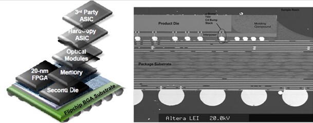
Infineon (GE) was the first company to commercialize its own eWLB packaging technology in an LGE cell-phone in early 2009 (see cross section below) Infineon’s chip is a wireless baseband SOC with multiple integrated functions (GPS, FM radio, BT…). The same eWLB product has also been in production in Nokia handsets since 2010.

Infineon wireless baseband SoC

LGE (wireless baseband), Samsung (baseband modem), and Nokia ( baseband modem and RF transceiver) have used eWLB in their cell phone products.

Deca Technologies

Chris Scanlan, VP of product management for Deca Technologies, recently gave a presentation entitled "Adaptive Patterning for Panelized Packaging" which described the company’s M-Series platform of embedded die (FOWLP) packaging.

Scanlan reported that their new process avoids the current pick-and-place positional accuracy and mold compound shrinkage issues inherent to current FOWLP processes. Die position accuracy of < 10μm and rotational accuracy of < 0.1° are typically required which in turn requires slow pick-and-place speed.

In Deca’s "Adaptive Patterning" process, die with copped studs (think copper pillar bump) are placed onto a carrier and molded into a 300mm wafer. Wafers are then removed from the carrier and planarized to reveal the copper studs. The wafer is imaged and the position of each die is imported into a proprietary software.

Connections are then made between the standard pad positions and the actual positions of the placed die. Deca has not disclosed the lithography process, but we do know that there are no traditional glass masks involved — which certainly helps explain their claimed fast turn around time. Industry conjecture is that some sort of laser processing is involved.

Customers have not been identified, although parent Cypress is probably one of them. Deca says it is "sampling to a limited set of customers with broader availability planned for 2013."

For all the latest in 3DIC and advanced packaging, stay linked to IFTLE……………………

IFTLE 123: Intel’s Bohr on 3DIC; Samsung DDR4 roadmap; Amazon to buy TI mobile chip unit? ; Communication will soon be king

Insight into Intel and 3DIC

For those of you that haven’t read Ed Sperling’s recent interview with Intel’s CTO Mark Bohr in Semi Manuf and Design, it contains some interesting comments on the 3D area [link]:

SMD: Where do stacked die fit into your roadmap?

Bohr: 3D stacked die have advantages, but only for certain market segments. You have to be very clear about what problem and what market segment you are trying to serve.

For a small handheld application where a small footprint and form factor are key and power levels are low, it probably makes good sense to use 3D stacking. For desktop, laptop and server applications where form factor isn’t as valuable and power levels are higher, 3D stacking has some problems that make it not an ideal solution.

And his thoughts on interconnect…

SMD: Is the interconnect [on chip] becoming more problematic?
Bohr: If you talk to a designer 10 years ago you would have heard the same thing. Maybe now they’re saying, ‘This time we’re really serious.’

SMD: How about new interconnect technology?
Bohr: It’s hard to replace copper and low-k other than by making lower k. But at least in the low-power cell phone market, stacking chips does help to minimize some of the interconnect issues, particularly between the logic and the memory chips.

SMD: You’re referring to through-silicon vias?
Bohr: Yes.

SMD: So if Intel is planning to get into that market, the company is experimenting with that technology right now?
Bohr: Yes, and we’ve been public about exploring TSV and 3D technology for a couple years. Although there are some challenging technology aspects, the real issue is cost. Doing TSVs and stacking chips — especially these custom Wide I/O chips — is expensive. So this might be a better engineering solution in terms of density, performance and power, but will the market bear the added cost? Not all markets will bear the higher cost.

Intel to use DDR4 with TSV starting in 2014?

Despite these comments, IFTLE would be remiss if we didn’t point out that rumors continue to swirl that Intel will use 3D stacked DDR4 memory in their Haswell-EX platform for enterprise computing [link].

Since Haswell will feature microprocessors with 12-14 cores, it will benefit from lower memory power consumption, higher memory bandwidth, and the memory capacity that DDR3 simply cannot provide. DRAM makers will make high-capacity DDR4 chips using through-silicon-via (TSV) technology that will allow to increase capacity of memory chips at a very fast rate. For servers, special switches will be introduced to avoid one module/one channel limitation.

Samsung DDR4

Indeed, Samsung demonstrated its next-generation DDR4 chips and memory modules at the Intel Developer Forum. Samsung showed a 300mm wafer of DDR4 die processed using 30 nm technology, insinuating that it could start production of DDR4 anytime the infrastructure became ready. Samsung plans to take DDR4 module speed for 2014 servers [like Haswell-EX?] to 2.666 GHz. Eventually, Samsung and Intel intend to boost the effective clock-speeds of DDR4 server memory modules to rather whopping 3.20GHz.

It is reported that in DDR4 memory sub-systems every memory channel will support only one memory module. To enable the highest-possible memory capacities, DRAM makers will use TSV stacking to make high-capacity DDR4 chips. Special switches will be used in server modules to avoid this module/one channel limitation.

Amazon in talks to buy TI’s mobile chip business?

Last month Texas Instruments announced plans to shift its focus away from its mobile processor business (~ $650M sales) and target broader markets such as industrial clients in the car industry, and Wall Street has speculated it could be sold.

Now, according to a report from Israeli newspaper Calcalist, Amazon is said to be in "advanced negotiations" to acquire this business from TI. This would be a step towards vertical integration for production of its Kindle tablets and could indicate an interest in entering the smartphones business. TI’s processors are used in Amazon’s Kindle Fire tablet. Amazon CEO Bezos reportedly touted TI’s industry strength at their new tablets recent launch. Speculation has existed for more than a year that Amazon could sell its own smartphone but Bezos has not addressed those rumors. The 1.0 GHz dual-core Texas Instruments 4430 OMAP application processor runs the Kindle Fire [link].

Reuters reports that Amazon declined to comment on the report. TI said it does not comment on rumors but said in an email to Reuters: "The smartphone market has become a less attractive long-term opportunity for TI … and we are re-profiling our investment accordingly."

If this sounds strange, why is it that different than Microsoft with its traditional business model of licensing operating systems to PC manufacturers, who will this month will launch the "Surface tablet," which it designed itself?

Communications to surpass computers as leading application for ICs

Our friends at IC Insights in their study, "IC market drivers 2013: A study of emerging and major end-use applications fueling demand for integrated circuits," forecasts communications applications to pass computer applications as the leading end-use for ICs starting in 2014 and lasting through at least 2016. The IC communications market is forecast to grow 9.2% in 2012 to $90.0 billion from $82.4 billion in 2011, and increase 11.7% to $100.5 billion in 2013, breaking the $100-billion level for the first time. The total communications IC market is forecast to reach $114.4 billion in 2014, 4.6% more than the $109.4 billion computer IC market. From 2011 to 2016, the communications IC market is forecast to grow by a cumulative annual growth rate (CAGR) of 14.1%, reaching $159.5 billion at the end of the forecast period. The communications segment accounted for 31.2% of worldwide IC sales in 2011 and the computer end-use segment 41.7%. By 2016, these two segments will flip-flop, with communications forecast to represent 42.2% of the total IC market, compared to 34.0% for the computer segment.

For all the latest on 3DIC and advanced packaging, stay linked to IFTLE…………