Siliconica

Monthly Archives: July 2013

Qualcomm Snapdragon 800 and Rockchip RK3188 – Battle of the Foundries!

The Snapdragon 800 (Qualcomm MSM8974) is Qualcomm’s leading-edge, low-power, mobile phone app’s processor with built-in 3G/4G LTE modem, using the latest Krait 400 CPU rated at 2.3 GHz and their 450 MHz Adreno 330 GPU. It was launched at this year’s CES International with this rather slick commercial.

Significantly, it is fabricated using the TSMC 28HPM (28-nm, High-Performance Mobile) process, which extends TSMC’s high-k, metal gate (HKMG) processing into the mobile space. Before this, all Qualcomm’s mobile chips were made with the TSMC 28LP polysilicon gate/SiON process; and to our knowledge, this is the first volume production part using 28HPM.

The 28HPM process sees a shrink in minimum gate lengths and SRAM cell size when compared with the 28HP process, and the inclusion of embedded SiGe source/drains for PMOS strain, which was not part of 28HPL.


TSMC 28HPM PMOS transistor

TSMC claims the technology can provide better speed than 28HP while giving similar leakage power to 28LP. The wide performance/leakage coverage apparently makes 28HPM ideal for applications from networking, tablet, to mobile consumer products.


The Rockchip RK3188 is targeted on tablets rather than phones, but it uses the GLOBALFOUNDRIES’ 28SLP (Super Low Power) process, their equivalent to TSMC’s 28HPM, aimed at mobile products. It is again a quad-core part, this time with ARM A9 CPUs running at 1.6 GHz, and quad-core ARM Mali GPUs rated at 600 MHz.


Rockchip RK3188 floorplan showing some of the major functional blocks

Rockchip has squeezed the functionality into ~25 sq. mm, less than a quarter of the size of the Qualcomm chip; not least because the A9 cores are noticeably smaller than the Qualcomm-designed Krait cores based on the ARM architecture, and of course there is no LTE.

GLOBALFOUNDRIES is obviously happy to have won the Rockchip business – their CEO Ajit Manocha specifically mentioned the partnership in his keynote talk at Semicon West:


The 28SLP process differs in a basic way from the TSMC 28HPM – GloFo is using their version of the Common Platform (GLOBALFOUNDRIES, IBM, Samsung) 28-nm process, which is a ‘gate first’ variety, i.e. a polysilicon gate is used with a HKMG stack at its base, doped to form NMOS and PMOS transistors. TSMC’s ‘gate last’ process uses a sacrificial polysilicon gate for all the processing up to the end of the source/drain processing, then the polysilicon is removed and replaced with distinct HKMG stacks which are tuned for NMOS and PMOS.

Like the other Common Platform HKMG processes, a SiGe channel is used in the PMOS transistors, though with GloFo’s own spin – none of these processes are the same from the different vendors.

Compared with the older 32-nm HKMG process used for AMD processors, the Rockchip uses bulk silicon, not SOI, and gate lengths, contacted gate pitches and SRAM cell size are shrunk, but in the same ballpark as TSMC’s process. There is no dual-stress liner or embedded SiGe source/drains to enhance PMOS performance, but this product is rated at 1.8GHz rather than TSMC/Qualcomm’s 2.3 GHz.


GLOBALFOUNDRIES 28SLP PMOS transistor

So we have two processes targeted at similar spaces, but with very different takes on how to do it. TSMC and Qualcomm are following the industry norm, supplying chips to a US company from Taiwan, and GLOBALFOUNDRIES and Rockchip have reversed the trend, supplying chips to China from the West, and it’s tempting to speculate they are from the Malta fab in New York.

A Dispatch from SEMICON West – Applied Materials Launches Epi System Focused on NMOS Strain

Flying in to SFO on July 7, I must have been one of many attendees delayed by the after-effects of the Asiana Airlines crash there the day before. In my case it was only an hour or so (i.e. as normal), but we couldn’t avoid seeing the remains of the aircraft as we landed. Despite the fact that the plane was burnt out, I couldn’t help being impressed that the main body of the plane had survived the impact, and of course all but two of the passengers survived – and they were outside the plane.

By coincidence I flew through Heathrow a week after another 777 did a belly-flop there a few years ago, and again I was impressed at the strength of the airframe – an engine had been ripped off a wing but otherwise it was pretty well intact – and fortunately in that case there was no fire, and no fatalities.

That’s hardly relevant to SEMICON West of course, but it’s hard not to get involved when we get that close to the statistics of travel accidents, be they road, rail or air.

Anyway – back to the show – or at least the pre-show events. Applied Materials (AMAT) had an analyst day on Monday, and in the morning they invited a few of us to some product launches. The one that caught my eye and ear was a new epi system focused on NMOS epitaxial source/drains to create channel strain, since that has been mooted as a next step for several years now, but not shown up in a production context.

The theory is that if you can get carbon and phosphorus to replace silicon atoms in the crystalline structure, because they are smaller than silicon, they will generate tensile stress in the crystal lattice. When it is deposited in cavities etched in source/drains the stress is applied to the channel. (Putting the larger germanium atoms in the lattice has the opposite effect, and creates compressive stress, an effect used since the 90nm node.)


Schematic of e-SiGe in PMOS (left), and e-Si:CP in NMOS (right) source/drains

The problem (as I understand it) has been that the carbon does not like staying in such substitutional positions, and it will abandon them as soon as it sees anneal temperatures, thus losing the stress effect. Phosphorus is happy to be substitutional, and has of course been used as a n-type dopant for decades, so I suspect the problem there is simply getting the concentration to a level sufficient to stress the lattice.

So on Monday AMAT launched the Applied Centura RP Epi system with an NMOS transistor application. To quote: “This capability supports the industry’s move to extend epi deposition from PMOS transistors to NMOS transistors at the 20nm node, enabling chipmakers to build faster devices and deliver next-generation mobile computing power.”


The Applied folks seem confident that once the epi is formed, the carbon can be kept stable and capable of applying the strain at the end of the manufacturing process. I quizzed them as to how this is done and apparently the keys are the quality of the clean after cavity etch (i.e. AMAT’s Siconi dry clean), plus millisecond annealing to minimize the thermal budget.

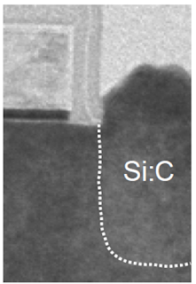
There is plenty of literature documenting the effect; at last year’s IEDM conference, IBM announced their 22nm server process, which uses embedded strain for both N- and P-MOS[1]. Together with nitride stress, they claim a 10 percent performance increase over the 32nm equivalent. I also asked the speaker there about the carbon stability, and he confirmed that they regard it as a manufacturable process.

Cross-section of NFET showing embedded Si:C Source/Drain Stressor [1]

It seems the time of e-Si:CP NMOS is here. Applied certainly hopes so: they estimate the available market at over $500M and expanding, and that revenue has doubled over the last five years, and they have more than 80 percent share. They see an incremental $250M in revenue from epi systems by 2016.

I’ve been waiting for epi-strained NMOS for the last couple of process generations, and had almost been convinced that it wouldn’t happen. Now we have to watch for it when we get the next 20nm parts!

[1] S. Narasimha et al., “22nm High-Performance SOI Technology Featuring Dual-Embedded Stressors, Epi- Plate High-K Deep-Trench Embedded DRAM and Self-Aligned Via 15LM BEOL”, IEDM 2012, pp 52 – 55.