By Dick James, Senior Technology Analyst, Chipworks
The much anticipated Samsung Galaxy S6 made an early appearance in our teardown labs last week, thanks to the diligent skills of our trusted logistics guru. We got our hands on the 4G+ version, the SM-G920I, with what Samsung claims is the world’s first octa-core 64 bit operating system. There is a wide array of industry buzz surrounding this flagship smartphone, but from my process-oriented point of view the focal point has to be on the Exynos 7420 application processor.
 |
| Samsung Galaxy S6 Teardown |
.png) |
| Galaxy S6 Motherboard |
Samsung Exynos 7420 Application Processor
The Samsung Exynos 7420 application processor is reportedly fabbed in Samsung’s 14 nm FinFET process. This is what Samsung has shown so far.
Which is not exactly specific! To start with, here’s the package marking of the package-on-package:

The layout of this is quite unusual – normally the memory marking (SEC 507 etc.) is in lines of text above the APU marking (7420 etc.), not in a diagonally opposed block. Which leads me into the speculation that maybe the 7420 is out of GLOBALFOUNDRIES, rather than a Samsung fab in Korea or Texas. Could ALB be short for Albany (NY)? Is the G in the lot code short for GLOBALFOUNDRIES? That all seems rather unlikely, but if Samsung wants to switch on the volume quickly in anticipation of huge volumes for the S6, what better way than to use three fabs? They did sound very confident in their last quarterly analyst call, saying that they expect 14-nm to be 30% of the LSI line capacity by year end. And there are lots of rumours about Qualcomm using the Samsung 14-nm process.
The die photograph and the die mark confirm the use of the Exynos 7420:
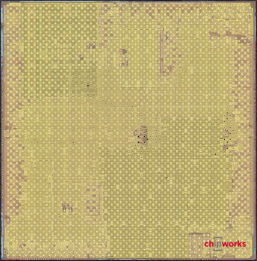

The functional die size is ~78 mm2, which compares well with the ~118.3 mm^2 of the Snapdragon chip used in the Galaxy S5, and the 113 mm^2 size of the 20-nm Exynos 5433. If the 7420 was a straight shrink of the 5433, we’d expect it to be 55 – 60 mm^2, but the back-end metallization stack is reported to be similar to the 20-nm planar process, so a full 50% shrink is unlikely (and the analog regions never shrink as well as digital anyway). We’ll have to wait until we see the floorplan to see how much functionality the two parts have in common.
Our guys in the lab made their usual exceptional effort in enabling us to see what the process looks like – within a few hours of getting the phone in-house, we have a decapsulated part and a cross-sectional sample under the microscope.
.png)
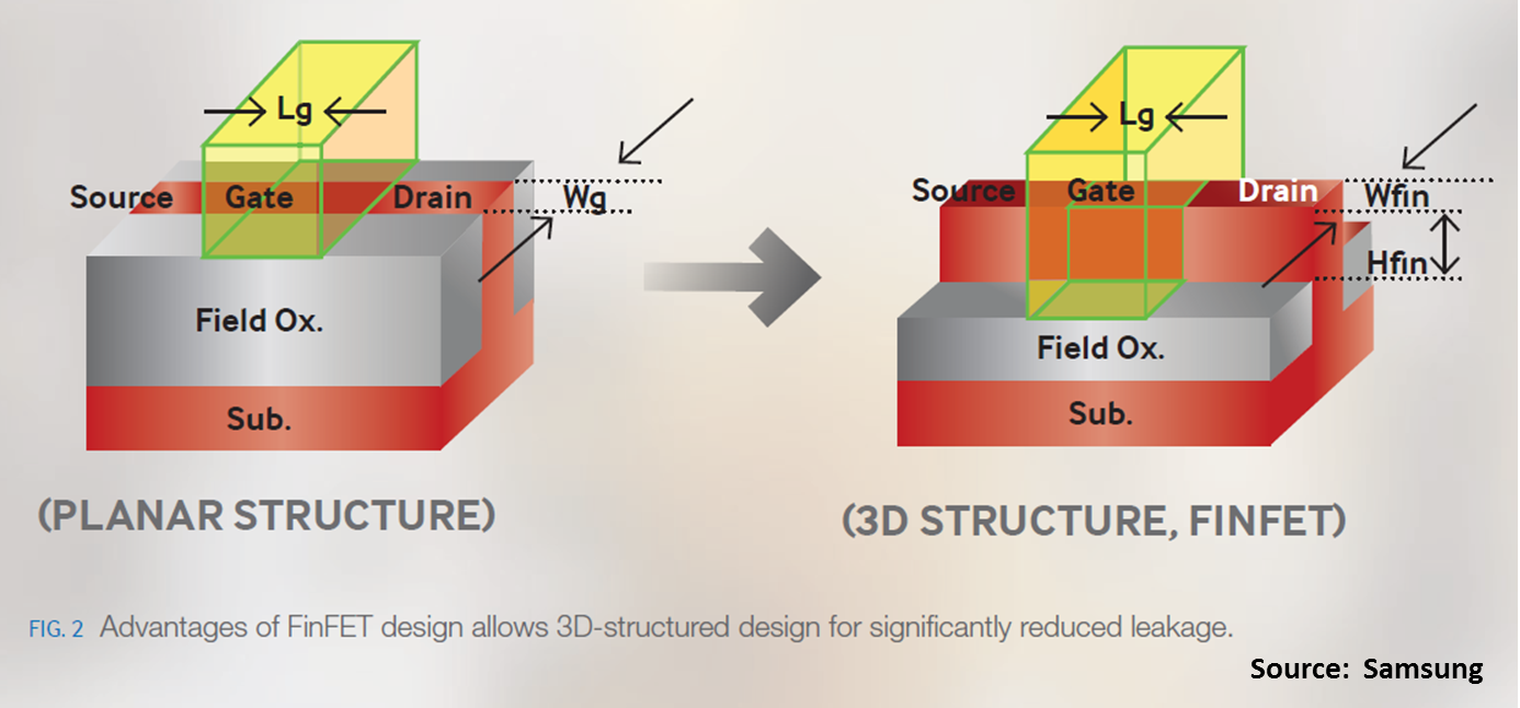
The Exynos 7420 uses 11 layers of metal, as you can see from the die seal cross-section above. Now let’s look at the transistors:
.png)
And we do have finFETs! This section is parallel to the fins, and across the gates. The bottoms of the contacts approximately indicate the top edge of the fin, and we are seeing the gates wrapped over and further down the sidewalls of the fin than the contacts appear to go. We will need another section orthogonal to this one to see if we have the type of epi growth in the source-drains that Intel uses.
This makes Samsung the second in line to get finFETs into volume production; they have successfully taken their 20-nm, first-generation, gate-last, high-k, metal-gate stack and adapted it to a first generation fin structure. We will need more detailed images to see whether the fins have vertical or sloped sidewalls, and how close to the Intel model they are, but those will come in the fullness of time when we have completed our full analysis and published our report.
Meanwhile, keep an eye on the blog!

Pingback: Samsung Galaxy S6 Edge pricier to build, cheaper to buy than comparable Apple iPhone 6 Plus | Solid State Technology
Really Appreciate this post, how can I make is so that I receive an update sent in an email when you write a new post?
Interested to know what application processor wil be used in next Galaxy S7.
Thanks Dick to share this informative article about Samsung Galaxy S6. Can you please tell me details about Galaxy S7 ?