Author Archives: insights-from-leading-edge

A SEMICON West snippet: AMAT launches new products, prepares for 450mm

SEMICON West is usually taken as a barometer for the industry, and my subjective impression is steaming along nicely, but no record breaking years coming up! According to Tom Morrow of SEMI, this year’s preregistrations were flat, but there about 10% more booths than last year.

I kicked off the show by sitting in at the Applied Materials (AMAT) press and analysts breakfast. As usual AMAT had a flurry of press releases preceding the show, and eight new products and product updates are being launched. A couple of years ago AMAT was putting more emphasis on their solar and display divisions, but this year silicon processing is again getting a high profile.

We had a series of presentations from Mike Splinter, Randhir Thakur, Steve Ghanayem, and Bill McClintock, and then Q-and-A from the analysts present.

Mike S. did the corporate overview: he saw the industry outlook as soft in the short term, but was basically upbeat since the industry drivers are still there — Moore’s law scaling, 3D transistors (in logic, flash and DRAM), and pushing them all, the mobile revolution. On the solar side, he predicted that solar modules will cross the $1/Watt threshold sometime this year, and hit $0.80/W next year, so cost reductions will help drive that end of the business.

Randhir Thakur then reviewed the product launches at the show, putting them into the context of the recent and upcoming changes in chip processing. Rather than list the new products, here’s the slide:

Steve Ghanayem focused on the Centura gate stack tool — essentially an ALD chamber has been added into the Centura system to give it high-k capability, all within vacuum:

He put a lot of emphasis on the cluster nature of the tool, so that the wafers only see vacuum between the process steps, claiming that exposure to atmosphere reduces mobility and increases threshold voltage spread.

The last technical presentation (Bill McClintock) covered off the new Black Diamond 3 (BD3) and Nanocure 3 extreme low-k dielectric and curing combination, giving a dielectric constant (k) of 2.2, down from k=2.5 in the previous generation. One of the things he pointed out (that I hadn’t thought about) was that the pre-metal dielectric layer at the bottom of the metal stack has to survive more than 150 process steps before wafer out in today’s 10-12 metal-layer processes, never mind the stresses of the packaging and assembly sequence.

So the challenges are formidable as the k-value is pushed down, to get both physical and material integrity; AMAT claims that by going to a closed-pore structure, with tighter pore size distribution, they can achieve k=2.2.

According to Bill, we can expect to see BD3 at the 22/15 nm nodes, so a couple of years yet before we see it in high-volume products.

Then we got to the Q-and-A session. Ironically, the first question was not about any of the product launches — it was about the spend on 450mm next year! Mike Splinter was reluctant to give a specific number, but he did say it would be "well over $100 million," mostly on early test systems in-house. Not exactly small change, all the same. A later question prompted the statements that "450 is going to happen," and that they are closely linked to the leading customers that will drive the move there. They are clearly now viewing 450mm as a strategic way of gaining market share when it does come.

Other questions covered off potential product expansion, and of course the future demand from foundries in what seems to be a softening market.

Randhir Thakur identified AMAT’s flowable CVD, Siconi clean and the Raider copper deposition tools as having found more applications than originally intended. The flowable CVD was targeted on one application, but ended up replacing CVD fill for STI, and other CVD steps with high conformality requirements. Siconi clean has evolved from a PVD clean, but has now moved into CVD and epi areas, any area where interfaces are critical. The Raider copper tool was developed from a Semitool product for packaging, but now has potential for damascene copper on die.

When it comes to the foundries, it appears that the fab shells are ready, and the message for the equipment companies is to be ready — things may be soft at the moment, but they could come back very quickly. Demand is controlled by the consumer market, and that has proved remarkably resilient considering some of the economic challenges in the last year or so.

All in all, an interesting session, both in the industry and technical senses. AMAT has the webcasts and presentations up on their investor website for until August 12, 2011.

TSMC HKMG is Out There!

I have to apologise for a hiatus in posting due to pressure from the day job, but this week is Semicon West week, so it seems appropriate to announce that we’ve started analysing TSMC’s 28-nm gate-last HKMG product, in this case a Xilinx Kintex-7 FPGA, fabbed in TSMC’s HPL process.

Having seen two generations of Intel’s HKMG parts (the 45-nm Xeon and 32-nm Westmere) using gate-last technology, it’s inevitable that we’ll compare those with the TSMC process.

The Kintex family is the mid-range group in the latest 28-nm generation 7-series of FPGAs from the company. These are optimised for the highest price/performance benefit, giving the performance of the previous Virtex-6 parts at half the price.
The Kintex-7 has eleven layers of metal (Fig. 1); the 1x layers run from metals 1-4, with a pitch of ~96 nm, the smallest we have ever seen.

Fig. 1 General Structure of Xilinx Kintex-7

Contacted gate pitch is ~118 nm in our initial analysis, with minimum gate length of ~33 nm, though since this is replacement gate there is no way of knowing absolutely the original poly gate width, which defines the source/drain engineering.

Plan-view imaging (Fig. 2) indicates that TSMC has implemented the restricted design rules that have been much discussed in the gate-first/gate-last debate. Regular, uni-directional patterning of functional gate and dummy gate lines helps out the lithography, but inevitably reduces packing density compared with Manhattan layout schemes.
Fig.2 Plan-View Image of Gates and Active Silicon
By the look of it, double patterning with a gate plus a cut mask has been used. FPGAs are usually laid out in a more relaxed manner than dense logic, so here we can see lots of dummy gates, and also dummy active regions.

The gate structure itself definitely has some similarities with Intel’s 45-nm, as we can see from figures 3 and 4.
Fig.3 Intel 45-nm (left) and TSMC/Xilinx 28-nm NMOS Transistors

Fig.4  Intel 45-nm (left) and TSMC/Xilinx 28-nm PMOS Transistors

In both it appears that the buffer oxide, the high-k layer and a common work-function material are put down before the sacrificial polysilicon gate. Then the source/drain engineering is performed, and dielectric stack deposited and planarized back to the polysilicon; and the sacrificial gate is removed, and the NMOS/PMOS gate stacks are put in and planarized.

Of course there are also differences – TSMC is not using embedded SiGe for PMOS strain, and there is an additional high-density metal layer in the PMOS gate. There is also no distinct dielectric capping layer in the TSMC structure, and there is an extra sidewall spacer (likely part of the source/drain tuning). The wafers are also rotated to give a <100> channel direction.
Intel stated that they applied stress to NMOS devices using the gate metal stack and the contacts; TSMC could be doing the same, although the contacts are spaced further from the gate edge. If there is PMOS stress, the mechanism is unclear, though it is possible that the extra high-density layer in the gate could be for that purpose. However, this part is fabbed in the HPL low-power process, and typically we do not see e-SiGe in such processes.
Analysis is ongoing – more details to come, and possibly a comparison with the AMD Llano gate-first HKMG part, that’s in our labs at the moment.

N.B. We are at Semicon West, at Booth 2337 – drop by and get a coupon for a free die photo!

Intel Goes Tri-Gate at 22-nm!

In a pair of press and analyst briefings this morning, Mark Bohr and Steve Smith announced that Intel will indeed be using a 3D transistor structure for their 22-nm product, settling one of the big questions about Intel’s process development over the last few years – do they stay planar or not? (And, incidentally, settling a bet between me and Scott Thompson – Scott wins!)

The big debate at IEDM last year about advanced CMOS was whether transistor structures would move to a 3D structure (finFET, tri-gate, whatever label you choose), or use ultra-thin SOI layers to attain fully depleted operation. The debate was not resolved – I was definitely left with the impression that the adherents in both camps held to their opinions, which probably means we will have two process groupings, much as we have with the gate-first/gate-last high-k/metal gate (HKMG) structures.

Intel have come down on the side of tri-gate – apparently the decision was taken in 2008, after their researchers had showed that the gate-last HKMG gate structure would work in 3D, and that the planar version could not give enough of a performance boost. So for the last three years they’ve been developing the process and getting it manufacturable for the production of the Ivybridge product line later this year.


Intel’s Research and Development Sequence to Reach the Tri-Gate 22-nm Node


I may have lost the bet about planar, but my gut feel that their HKMG process could be extended to 22-nm seemed to be right, since Mark confirmed that they are using gate-last (replacement gate) technology, with evolutions of existing NMOS and PMOS strain technology. Immersion lithography and double patterning will be used where necessary, and no extra mask layers are needed so the additional cost is only 2 – 3%. And apparently it’s scalable to 14 nm!

The schematic below shows a gate formed on three sides of three fins, to give more drive strength than available from one fin:

Schematic of Tri-Gate Across Three Fins (Source – Intel)

When translated to gate-last HKMG, it looks like this in this Intel image from 2007 (the section is through three gates, with three fins buried under oxide running across the field of view):

Gate-Last HKMG Tri-Gate Transistors (Source – Intel)

And now a new image from today’s briefing, showing an array of transistors with six fins in the centre, and some with two fins at the top right and bottom left:

Intel Tri-Gate Transistors (with STI and gate mold oxide removed) (Source – Intel)

Clearly this means a whole new set of design and layout paradigms, and we can see evidence here of double patterning using fin and gate masks, with cut masks to define the individual fins and gates.

During the briefings, Mark also scotched the rumour that appeared a few weeks ago about a hybrid process, where the SRAM is tri-gate and other areas are planar – all of the chip area will be tri-gate. In addition a parallel SoC process is being developed so that the Atom line of products can be extended to 22-nm.

For us commentators, going tri-gate was always a possibility for Intel; they have been publishing papers on the topic for almost ten years, with a flurry of them five years ago – here’s an image from a press briefing in 2006:

TEM Image of HKMG Tri-Gate Transistor, Sectioned Through the Fin(Source – Intel)

Their R-D-M (Research-Development-Manufacturing) methodology has been well established for quite a while now, and enabled them to keep to their schedule of a new process generation every two years. Based on comments today, we can expect to see 22-nm production in the second half of this year, and product on the shelves in the New Year.

Then we’ll see what it really looks like!

A Shameless Plug for ASMC

Winter is finally starting to fade in Ottawa, and the early signs of spring are showing. The maple sap is running, the first migrant birds have arrived, the frogs are peeping, and we have evening daylight. On the conference calendar, spring means that ASMC (IEEE/SEMI Advanced Semiconductor Manufacturing Conference) is on the horizon, this year in Saratoga Springs, New York on May 16 -18. There, spring should be well advanced, and it will be a great time of year to visit the Empire State.

As the name says, ASMC is an annual conference focused on the manufacturing of semiconductor devices – in this it differs from other conferences, since the emphasis is on what goes on in the wafer fab, not the R&D labs, and the papers are not exclusively research papers.

I’m plugging ASMC because it seems to be one of the more under-rated conferences, unlike IEDM and the VLSI symposia, which get the media attention for leading-edge R&D and processes. However, it’s the nitty-gritty of manufacturing in the fab that gets the chips out of the door, and this meeting discusses the work that pushes the yield and volumes up and keeps them there.

I always come away impressed by the quality of the engineering involved; not being a fab person myself any more, it’s easy to get disconnected from the density of effort required to equip a fab, keep it running and bring new products/processes into production. Usually the guys in the fab only get publicity if something goes wrong!

This year, in addition to the 50-plus papers, there are keynotes from Norm Armour of GLOBALFOUNDRIES (GloFo), Gary Patton of IBM, and Peter Wright of Tradition Equities, as well as a panel discussion on partnerships in semiconductor manufacturing, moderated by Dave Lammers. There are also tutorials, on 3D (by James Lu of Rensselaer Poly), and EUV (by Obert Wood of GloFo), and an invited session of ISMI papers.

The technical sessions include:

  • Factory Optimization
  • Advanced Metrology
  • Advanced Equipment, Materials and Processes
  • Advanced Process Development and Control
  • Advanced Lithography
  • Defect Inspection and Yield Optimization
  • Data Management

Of course, I’m biased to some extent because we’ll be giving a paper there again. I can’t make it this year, but a colleague of mine, Ray Fontaine, is presenting on "Recent Innovations in CMOS Image Sensors". This will be the seventh year running we’ve given a paper, the manufacturing and equipment engineers that attend seem to like seeing what their competitors are doing. In this case Ray will run through some of the changes in the camera chips that we all take for granted in our phones these days.

Other papers that caught my eye may give us some clues as to what to expect in the lithographic field; the IBM/Glofo/Toshiba alliance has one on contact patterning strategies (paper 6.3), and another cooperative paper by IBM/JSR/KLA Tencor/Tokyo Electron on double patterning (6.1), and an IBM/ASML contribution on advanced overlay control (2.5). And on the materials processing side, there are three papers on low-k dielectrics from GloFo/KLA Tencor (2.4), UAlbany/Air Liquide (3.5), and Novellus (poster in session 4); and a couple on nickel silicide by GloFo (5.3) and Ultratech (poster in session 4); and a clue to the mysteries of high-k dielectrics from UMC/National Cheng Kung U (3.4).

More stategically aimed discussions are by Infineon (1.1) on the challenges in having a global supply chain, Sumita Bas of Intel will be speaking on sustainable/green in the chip business (1.3), and two talks by SEMATECH, one on 450 mm manufacturing (ISMI session), and the other on 3D/TSV manufacturing (3.1).

Out of the conference room, there’s a poster session and reception on the Monday evening, and on the Tuesday, Dave Lammers’ panel session, "Models for Successful Partnerships in Semiconductor Manufacturing". Partnership is one of the buzzwords in chipmaking these days, and the panelists we have should know it well; Ari Komeran from the industry development side of Intel, Michael Fancher from Albany, Olivier Demolliens, head of LETI-NANOTEC in France; and Dr Walid Ali, from ATIC in Abu Dhabi.

After the panel session, what could be a highlight of the conference, a tour of the Luther Forest Technology Campus, including a look at GLOBALFOUNDRIES (Norm Armour’s) new Fab 8, followed by a reception at the Canfield Casino.

Register soon – rates go up on May 8th!

Panasonic Gate-First HKMG also First Out of the Gate

As I suggested a few months ago, we put some credence in Panasonic’s press release last September that they would be shipping their first 32-nm HKMG parts last October. Samsung had announced their Saratoga chip, and both Altera and Xilinx have displayed silicon from TSMC, but until last Friday (18 March), none have said that they were shipping product. As of Friday Xilinx announced that they were shipping their Kintex-7 product, the first of their 7-series of FPGAs.

Earlier this month our faith in Panasonic was rewarded, and we found the chip! It took a few false starts buying Panasonic products that we tore down and threw away, but now we have a verified 32-nm, gate-first, high-k metal-gate (HKMG) product. The supply chain was a bit longer than we had hoped, but as promised the chip was shipped with a week 41 date code, in October.

So, for the curious, this is what a transistor looks like:

Panasonic’s 32-nm HKMG NMOS Transistor

We can see the TiN metal gate at the base of the polysilicon, and the thin line of high-k at the base of the TiN. Also noticeable are a dual-spacer technology (sometimes referred to as differential offset spacers), and a thin line of nitride over the source/drain extension regions (possibly indicating a nitrided oxide under the high-k). The salicide is the usual platinum-doped nickel silicide. Less visible are mechanisms of applying strain, other than the nitride layer over the gate; embedded SiGe and dual-stress liners are not used.

All of which is typical for Panasonic – their 45-nm product did not appear to use any enhanced strain techniques, and the only concession to PMOS enhancement was wafer rotation to give a 1-0-0 channel direction. The emphasis is different from Intel; rather than raw performance, the targets are increased integration, die size reduction/reduced cost, and now we have high-k, reduced leakage/lower power. The September press release does say that transistor performance is improved by 40%, but it also claims 40% power reduction and a 30% smaller footprint.

Here’s a 45-nm transistor for comparison:

Panasonic’s 45-nm Generation Transistor

And, for good measure, Intel’s 32-nm device:

Intel 32-nm NMOS Transistor

The part itself uses a nine-metal (eight Cu, one Al) stack with a hybrid low-k/extra-low-k stack. Die size is ~45 mm2 in a conventional FC-BGA package. Minimum metal pitch is specified as 120 nm [1], and we have found 125 nm in our early investigations.

Panasonic 32 nm General Structure

Analysis is ongoing – stay tuned for more details, and of course we’ll be doing reports!

[1]S. Matsumoto et al., Highly Manufacturable ELK Integration Technology with Metal Hard Mask Process for High Performance 32nm-node Interconnect and Beyond”, IITC 2010

Apple’s A5 Processor is by Samsung, not TSMC

Forty-eight hours ago we obtained an iPad 2 and brought it back to the lab, and took it apart to have a look at Apple’s A5 processor chip. We’ve come to the conclusion that the main innovation in the new iPad is the A5 chip. Flash memory is flash memory (multi-sourced from Samsung and Toshiba in the iPads we’ve seen), the DRAM in the A5 package is 512 MB instead of 256 MB, and the touchscreen control uses the same trio of chips as the iPad 1 – not even a single chip solution as we’ve seen in the later iPhones. And the 3G version uses the same chipset as the Verizon iPhone launched a few weeks ago. This is the mother-board from a 32-GB WiFi-only iPad 2:

Motherboard from 32-GB iPad 2


The A5 can be seen in the centre of the board. If we look at the package we can identify the Apple’s APL0498 marking for the A5 (the A4 is APL0398), and also 4 Gb of Elpida mobile DRAM. Date codes are 1107 for the A5 and 1103 for the memory – only a few weeks in the supply chain here!

Apple A5 from iPad 2


The x-ray images show us that we have the usual package-on-package (PoP) structure, with two memory chips in the top part of the PoP, and the APL0498 processor on the lower half.

X-Ray Image of A5 Package-on-Package

The two rows of dense black dots on the outside of the image are the solder balls from the memory chips in the top half of the package (connecting with the bottom half), and the less dense dots are the solder balls on the bottom half of the package connecting the A5 chip to the iPad board below. If you squint really hard you can see smaller dots about five rows in from the edge which are the flip-chip solder balls on the A5 die – and they take up quite a large proportion of the area, showing that this is a good-sized die.
The die photo and die mark are shown here:
Die Photo of Apple’s A5 Chip from the iPad 2
APL0498E01 Die Mark of Apple A5 Chip


The x-ray is right – the A5 die is more than twice as large as the A4, at 10.1 x 12.1 mm (122.2 mm2), vs 7.3 x 7.3 mm (53.3 mm2) – here’s the A4 chip for comparison:
Apple A4 Die Photo


Given that the A5 is a dual-ARM core, and has more graphics capability than the A4, more than doubling the size is to be expected, but it’s also a clue that this is still made in 45-nm technology.
So after the web speculation that TSMC might be fabbing the A5 rather than Samsung, we had to take a look, and the quickest way is to do a cross-section and compare it with the A4 from last year’s iPad.
So here’s the A5:
SEM Cross-Section of Apple A5
It’s a nine-metal layer part, with eight levels of copper and one aluminum. Zooming into the transistor level:
SEM Cross-Section of Transistors and M1 in A5 Processor
And now the A4:

SEM Cross-Section of Transistors and M1 – M4 in A4 Processor

At this scale even electron microscopes start to run out of steam, so not the clearest of images in either case, but good enough to see the similar shape of the transistor gates and the dielectric layers. So at least this sample of the A5 is fabbed by Samsung, just as all Apple’s processor chips have been for the last while.

Many thanks to the guys in the lab who’ve worked through the weekend to get this information – Chipworks is not really in the media business, but there’s always a buzz when a hot new consumer part comes out.

And on a different note, commiserations and condolences to our Japanese colleagues, they have much more important things of concern than the details of the iPad 2.

How to Get 5 Gbps Out of a Samsung Graphics DRAM

It’s well known that electronics games buffs like their image creation as realistic (or at least as cinema-like) as possible, which in image-processing terms means handling more and more fine-grained pixel data as fast as possible. That means more and more stream processors and texture units in the graphics processor to handle parallel data streams, and faster and faster memory to funnel the data in and out of the GPU.

We recently pulled apart a Sapphire Radeon HD5750 graphics board, containing an AMD/ATI RV840 40-nm GPU, running at 700 MHz, and supported by eight Gb (1 GB) of Samsung GDDR5 memory. This card is a budget card, but the ATI chip still boasts 1.04 billion transistors, 720 stream processors and 36 texture units, can compute at ~1 TFLOPS with a pixel fill rate of 11 Gpixel/s, and can run memory at 1150 MHz with 74 GB/sec of memory bandwidth. I’m not a gamer, but those numbers are impressive to me!

When we started looking at the memory chips, and decoded the part number, we found that we had Samsung’s fastest graphics memory part, claimed to run at 5 Gbps. Graphics DRAMs are designed to run faster anyway, but 5 Gbps is three times faster than the fastest regular DDR3 (Double-Data Rate, 3rd Generation) SDRAM, which can do 1.6 Gbps.*

So what makes this one so blazing fast? Beginning with the x-ray, the difference between a Graphics DDR5 when compared with a 1Gb DDR3 (K4B1G0846F-HCF8) part starts to show up. If we look at an x-ray of the DDR3 chip, we can see that it has the conventional wire-bonding down the central spine:

Plan-View X-ray of Samsung 1 Gb DDR3 SDRAM

When we compare the K4G10325FE-HC04 GDDR5 we can see first that it’s a flip-chip device (no wires), and if we squint hard enough we can also see that the bumps are distributed across the die as well as along the spine.

Plan-view X-ray of Samsung 1 Gb GDDR5 Part from ATI Radeon

This is confirmed in the die photograph:

Die Photo of Samsung 1 Gb GDDR5 SGRAM

Which compares with the die photo of the 1-Gb DDR3:

Die Photo of Samsung 1 Gb DDR3 SDRAM

The die layout is clearly optimized to reduce RC delays from the memory blocks to the outside world. The next question for me is the nature of the flip-chip bonding; is it regular solder bumps or gold stud bumps? A cross-section solves that problem – solder, on plated-up copper lands.

Cross-sectional Images of Samsung GDDR5 Chip in Package

A quick x-ray spectroscopy analysis tells us that the solder is silver-tin lead-free, confirming the package marking.

So the answer to our question is actually fairly obvious – lay out the die to reduce input/output line lengths, and thereby RC delays on the chip, and replace bond wires with bumps to minimize RC delays in the package. A nice exposition of basic principles used to optimize performance.

The next step would be to co-package the memory chips with the GPU to reduce lateral board delays, and we have seen that in products such as the Sony RSX chip in the PS3 gaming system. And after that, lay out the GPU for through-silicon vias – but that will be another story..

For those with an interest in the memory interface circuitry in the RV840, my colleague Randy Torrance has posted a discussion on the Chipworks blog.

* At the time of writing!

Samsung’s 3x DDR3 SDRAM – 4F2 or 6F2? You Be the Judge..

We recently acquired Samsung’s latest DDR3 SDRAM, allegedly a 3x-nm part. When we did a little research, we found that the package markings K4B2G0846D-HCH9 lined up with a press release from Samsung last year about their 2 Gb 3x-nm generation DRAMs. My colleague at Chipworks, Randy Torrance, popped the lid to take a look, and drafted the following discussion (which, amongst other things, raises the perennial question for us reverse engineers – how do you define a process node in real terms?). Now read on..

The first thing we did was measure the die size. This chip is 35 sq mm, compared to the previous generation 48-nm Samsung 1Gb DDR3 SDRAM, which is 28.6 sq mm. Clearly this 2 Gb die is much smaller than 2X the 48-nm 1 Gb die, so our assumption that we have a 3x nm part looks good so far.

Die Photo of Samsung 3x DDR3 SDRAM

Next we did a bevel-section of the part to take a look at the cell array. We were surprised with what we found. The capacitors are laid out in a square array instead of the more usual hexagonal pattern (see below), and the wordline (WL) and bitline (BL) pitches are both about 96 nm. The usual method of determining DRAM node is to take half the minimum WL or BL pitch. That places this DRAM at the 48-nm process node, the same as the previous Samsung generation of 48 nm. So why does the die size look like it should be a smaller technology? For this we need to look at cell size.

Plan-View TEM image of Capacitors in Samsung 3x-nm SDRAM

But before we get into that we should discuss the DRAM convention of describing the memory cell size in terms of the minimum feature size, F. Historically, DRAM cells have used an 8F2 architecture for many years. This allows for the use of a folded bitline architecture, which helps reduce noise. In order to decrease cell area, companies came out with the first 6F2 cells in 2007; this 6F2 architecture is now used by all major players in the DRAM market. The guys at ICInsights published the plot below in the latest McLean report which nicely illustrates the progress:


DRAM Cell Size Reduction Through the Years
The 48 nm SDRAM has a cell size of ~0.014 sq µm. This new SDRAM has a cell size of 0.0092 sq µm. Clearly this cell is much smaller than the 48 nm generation. If we take the half-WL pitch as the minimum feature size (F), we get an F of 48 nm for this process. The cell area of 0.0092 sq µm is exactly 4 x F, squared, 4F2. Is this the world’s first 4F2 cell? From this point of view it certainly appears so. The cell is four times the size of the minimum feature, squared. But, there are other ways of looking at this.
A 4F2 architecture is defined as having a memory cell at each and every possible location, that being each and every crossing of WL and BL, with the cell being 2F x 2F. This is in fact what we see on this Samsung DRAM, so maybe we are looking at the first 4F2 architecture. But let’s look just a bit closer to be sure.

We compared the poly and active layout under the array between the 48 nm SDRAM and this new one. The images are shown below. As can be seen, both have very similar layouts. The angle of the active silicon (diffusion) direction is about the same. The active areas are ovals. Each diffusion has two wordlines crossing it. There is a gap between all the active areas, such that a third WL does not cross active on this diagonal active direction.

Samsung K4B1G0846F 48nm 1 Gb DDR3 SDRAM,
Poly and Active Area Image under Cell Array

Samsung K4B2G0846D 2Gb DDR3 SDRAM,
Poly Remnants and Active Areas under Cell Array
This new DRAM clearly has a very similar cell layout to the previous one. In both cases the wordlines do not have a transistor under them at every possible location that a transistor would fit. Rather, one of every three possible transistor locations is filled with a break in the diffusion stripe. This is really a better definition of a 6F2 cell, since in a 6F2 architecture 2/3 of the WL/BL intersections are filled with storage cells. As we noted above, a 4F2 cell really should have transistors at every possible transistor location.


When we look at the pitch of the diffusions in this new DRAM, we see it is much tighter. In fact, along the WL direction the diffusion pitch is now 64 nm, whereas in the 48 nm SDRAM this pitch was 96 nm. So if you take half the minimum pitch in the chip as the node, this is a 32-nm part (ITRS 2009 still defines F as half the contacted M1 pitch, which would be 48 nm).

So, do we have a 32 nm node, and a 6F2 architecture? Maybe. The only issue is that if we use 32 nm as F, then when we plug that into the 6F2 equation we get 0.0061 um2 as the cell size. However, the cell size is actually 0.0092 um2. If we use that number and use the equation to calculate F we find that F=39nm. Soâ??¦ do we call this a 32 nm or a 39 nm node? It depends how you calculate it – either way it’s a 3x!

So, although it’s a little disappointing that I don’t think we can announce the worlds first 4F2 DRAM, we can announce the worlds smallest node, 32 or 39 nm, production 6F2 DRAM.

Samsung have had to put in a few process tweaks to squeeze the cells into the much smaller area, mostly at the transistor and STI level. We’re still looking at it, so we may not have the whole story yet, but some of what we’ve seen so far is:
• Ti-? (likely TiN)-gate buried wordline transistors
• STI filled with nitride in the array
• Bitlines at the same level as peripheral transistors
Our up-coming reports will give many more details on this fascinating part.

Common Platform Goes Gate-Last – at Last!

At the IBM/GLOBALFOUNDRIES/Samsung Common Platform Technology Forum on Tuesday, Gary Patton of IBM announced that the Platform would be moving to a gate-last high-k, metal-gate (HKMG) technology at the 20-nm node.

At the 45- and 32-nm nodes there has been a dichotomy between gate-last as embodied by Intel, TSMC, and UMC, and gate-first, promoted by the Common Platform and others such as Panasonic. (Though, to be realistic, Intel’s is the only HKMG we’ve seen so far, and the only 32-nm product.)

The split puzzled me a bit, at least for high-performance processes, since Intel have clearly shown that for PMOS, compressive stress using embedded SiGe source/drains is a really big crank that is enhanced by removal of the dummy polysilicon gate in the gate-last sequence. In fact, in their 32-nm paper at IEDM 2009 [1], the PMOS linear drive current exceeds NMOS, and the saturated drive current (Idsat) is 85% of NMOS. This trend is shown below:


Intel Drive Currents at the Different Nodes [1]

 We can clearly see the narrowing between NMOS and PMOS drive currents at the 45-nm node, namely with the start of replacement gate (gate-last) technology.

So it seems obvious that to have high-performance PMOS, gate-last is the way to go; admittedly IBM and their allies have been using compressive nitride for PMOS, which Intel never have (at least to my knowledge), but there are limitations to that – now that contacted gate pitch has shrunk to less than 200 nm, there is not much room to get the nitride close to the channel – a problem that will increase with further shrinks.

So in a way it’s not surprising that the Platform has made the change; nitride stress is running out of steam, and gate replacement offers improved compressive stress for PMOS, and other stress techniques for NMOS (Intel builds some stress in with the gate metal).

Gary Patton said that IBM have been evaluating gate-last in parallel with gate-first since 2001, and it’s logical that they and their partners should. Both GLOBALFOUNDRIES and Samsung have published on gate-last, so there has been some evidence of checking out the parallel paths.


GLOBALFOUNDRIES PMOS and NMOS (right) Gate-Last Transistors [2]


Samsung Gate-Last Transistor [3]

Patton said that they selected gate-first in 2004; judging by their papers, Intel took their decision in 2003. The rationale that he put forward for the change to gate-last involved four points:

  • Density – gate-first has higher density, since gate-last requires restricted design rules (RDRs). That prevents orthogonal layout, requiring local interconnect; but at 20-nm RDRs are needed for lithography, so that advantage disappears.
  • Scaling – it’s easier to scale without having to cope with RDRs; at 20-nm there’s no choice.
  • Process simplicity – it’s obviously easier to shrink if you can keep the same process architecture, whether it be to 32- or 20-nm
  • Power/performance – the gate last structure allows strain closer to the channel, increasing performance; but fully contacted source/drains increase parasitic capacitance, slowing things down. According to Patton these net each other out for a high-performance process, making the gate first/last decision neutral. For low-power processes, strain is not used at the 45/32-nm nodes, so gate-first gives better power/performance metrics.  At 20-nm strain has to be used for low-power, and with the need for RDRs and local interconnect, the balance shifts in favour of gate-last.

So it appears that for the Platform the equation between pure transistor performance, process convenience, and power/performance made gate-first the choice at 45/32/28-nm, but at 20-nm the balance changes to make gate-last the way to go. That was likely influenced by the adoption of immersion lithography between 65- and 45-nm, which reduced the need for RDRs.

Intel presumably did similar sums during their 45-nm development, and figured that using RDRs would save them the cost of going to wet lithography at that node, and at the same time adopting gate-last technology would give them a manufacturing advantage. (My speculation is that they had also concluded that their version of gate-last may be more complicated to start up, but would prove to be more manufacturable than struggling with the instabilities that seem to go with the gate-first work-function materials. I guess they’ve proved that!)

Interestingly, now that Intel is using immersion lithography at 32-nm, they have loosened up on the RDRs, there’s more flexibility in the layout than there appeared to be at 45-nm.

I have to congratulate the Common Platform marketing guys on putting up a live webstream of the Technology Forum – I couldn’t get to the event itself, so wouldn’t have been able to comment without it. The stream will be available until April 29, so if you want to see Gary Patton for yourself, you can.


Screen Shot of Gary Patton of IBM at the Common Platform Technology Forum

Unfortunately, talking to my journalist colleagues, no slide sets were available, even at the press conference, so watching the stream occasionally leaves you puzzled as to what’s being talked about; and as you can see from the screen shot above, the room screens were carefully blanked out for the camera. Also, the breakout sessions in the afternoon were not streamed, or if they were, not recorded for later viewing. Still, kudos to the Platform for the live stream we did have, and the pre-recorded panel sessions!

From Gary’s and other comments at the Forum, it’s clear that the first HKMG products will be launched at 32-nm, and 28-nm will be following along fairly soon after. We can’t wait to see some!

For those waiting for more details if last year’s IEDM, I will finish my review; there were 36 sessions with 212 papers, so not a small task to do conscientiously, the Christmas break interrupted things, and there have been distractions since (like the Forum!), but I will get there!

References:

  1. P. Packan et al., High Performance 32nm Logic Technology Featuring 2nd Generation High-k + Metal Gate Transistors, IEDM 2009, paper 28.4, pp. 659 – 662
  2. M. Horstmann et al., Advanced SOI CMOS Transistor Technologies for High-Performance Microprocessor Applications, CICC 2009, paper 8.3, pp.149 – 152
  3. K-Y. Lim et al., Novel Stress-Memorization-Technology (SMT) for High Electron Mobility Enhancement of Gate Last High-k/Metal Gate Devices, IEDM 2010, paper 10.1, pp. 229 – 232

IEDM 2010 Retrospective – Part 1

The International Electron Devices Meeting started its 56th session last week on Sunday in San Francisco. This year the program appears to more academic than in previous years, and this was confirmed by the conference chair in his opening address – only 145 submissions out of a total of 555, an all-time low as a percentage. Attendance was guesstimated at ~1500, again lower than earlier years on the west coast. On the other hand, the atmosphere is noticeably more upbeat than last year, and there are plenty of industry attendees.

Sunday was short course day, well attended with ~580 participants. There were two courses, “15nm CMOS Technology”, and “Reliability and Yield of Advanced Integrated Technologies” – I sat in on the reliability session and brought myself up to date on the issues now that we’re into the deep nanometer era. The European weather had its effects, the chair Guido Groeseneken was stuck in Amsterdam due to snow, and Werner Weber had to take over. So far Europe has had a worse winter than I’ve had to cope with in Canada!

The course had some useful stuff for me, not being involved in reliability – it’s not something we need to worry about when we take stuff apart! We had a good review of time-dependent breakdown and n- and p-BTI by Ben Kaczer of IMEC; some interesting new analytical work on changes in low-k dielectrics from Shinichi Ogawa; a surprisingly optimistic review of ESD techniques by Christian Russ of Infineon (apparently strain can actually improve ESD performance!); and the day was rounded out by consecutive reviews of different approaches to reliability by design mitigation by Ashraf Alam (Purdue) and Andrzej Strojwas (PDF Solutions).

On the 15-nm course, the gossip I heard was that folks were pleasantly surprised that there is a roadmap to get there. Tom Skotnicki convinced people that the thin SOI/thin BOX solution will work better than finFETs – at least he didn’t get snowed in!

Monday morning we got into the plenary session, starting with Kinam Kim of Samsung. He started off by predicting that DRAM will get into the 10-nm generation, though not for another ten years, by using new variants of MIM stacked capacitors, and evolving through buried wordlines to vertical access transistors with buried bitlines.

Then he moved on to flash, detailing the problems created by a shrinking number of electrons on the floating gate, the increasing aspect ratio of the gate stack, and the inability to scale the dielectrics. We’ll still get to the 1x node, but after that 3D cell structures will appear, likely with charge-trapping technology. We had a brief reference to ReRAM as universal memory (though as the Scots say, I ha’e ma doots), but it’ll be a while before we get there.

Then we moved into logic, with the many variants possible below 20-nm – finFETs, hybrid chips with III-V devices on silicon, graphene, etc, and a quick run-through of the various stacking options such as package-on-package and (of course) TSVs; the latter was apt in the context of the day’s announcement of an 8-GB DIMM using TSVs.

The second plenary talk was equally interesting in pointing up the actual and potential use of semiconductors in making electrical consumption more efficient, from generation through transmission to end usage. Examples given were whole-wafer thyristors used for switching HVDC lines (apparently DC transmission is much more efficient than AC, and there’s a 1400-km, 800KV line in China), and at the other end of the scale a server power supply with 99% efficiency.

Schematic (top) and Image of Whole-Wafer Laser-Triggered Thyristor Switch (Source: Infineon/IEDM)

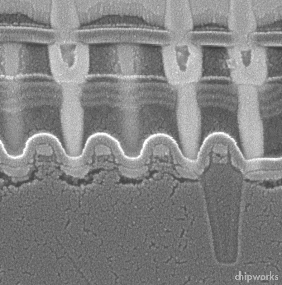
The afternoon memory session started off with Samsung’s 27-nm NAND flash paper (5.1). It amazes me every time that we see a new generation of NAND flash that the cell is essentially a shrink of the classic control gate/floating gate structure, even though we’re now counting electrons.

That’s what we have here:

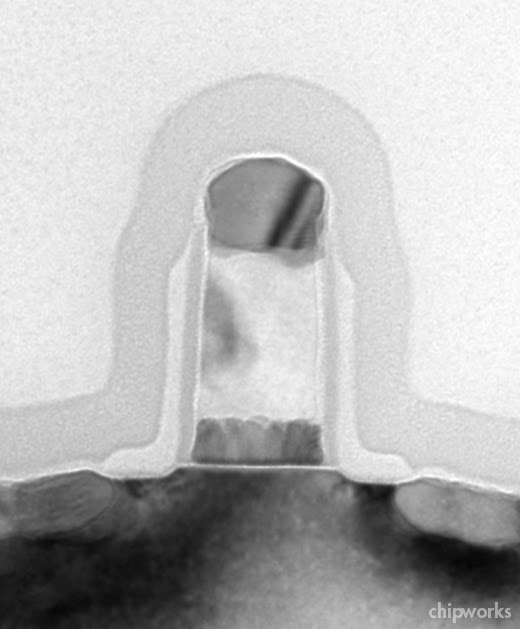
Samsung 27-nm (left, source: Samsung/IEDM) and 35-nm NAND Flash Gate Structures

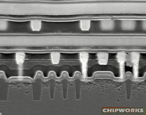
I’ve included an image of the 35-nm cell for comparison, to show the essentially similar structures, control gate/wordline (CG) on top, and floating gate (FG) below. Below is an orthogonal section along the line of the control gate, again with the 35-nm part for comparison.
,

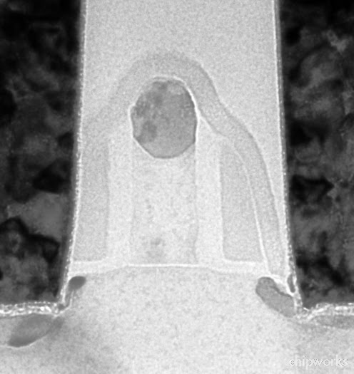
Section Parallel to Control Gate of 27-nm (left, source: Samsung/IEDM) and 35-nm NAND Flash

The main difference we can see, apart form the dimensional shrink, is the increase in the aspect ratio of both gates. This deliberate, to maintain the coupling ratio between the control gate and floating gate, and also the resistivity of the wordline to minimize RC delay (8 ohm/sq is quoted).

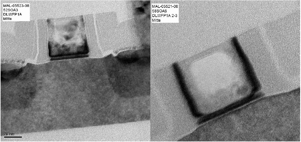
One of the changes discussed in the paper is a novel tunnel oxidation process (i.e. between FG and substrate) that conserves the boron doping in the channel and raises the Vt by ~0.5V. This tweak is useful for a number of performance considerations:

  • the reduced Vt shift between a programmed state and an un-programmed state helps reduce the capacitance linkage between adjacent floating gates
  • it improves endurance by reducing the fringing field between the top corner of the active silicon and the control gate, where it comes down close to the substrate between floating gates – during programming the high voltage across this gap can cause tunneling to the CG, which can degrade the tunnel oxide and affect endurance.
  • it improves the data retention by reducing charge leakage off the floating gate

This “novel tunnel oxidation” is not described in detail, but if we blow up their somewhat fuzzy TEM image, and compare again with the 35-nm chip, it looks as though the tunnel oxide has been nitrided.


Tunnel Dielectrics of 27-nm (left, source: Samsung/IEDM) and 35-nm NAND Flash


A question was asked at the end of the paper about the novel oxidation, and of course the presenter didn’t give a direct answer, but an implant step was mentioned; a locking implant for the boron seems likely.

I’ve gone into more detail about this paper than is probably sensible in a blog, but it was the first paper of the regular sessions, and the detail of getting 64Gb of cells that work onto one die can’t help being fascinating to a process geek like me.

Next up (5.2) was Micron’s 25-nm flash, which they announced almost a year ago. A different take on the same challenges, Micron have used air-gap technology to mitigate the capacitance linkage between adjacent gates, and adacent bitlines (see below).

"Air Gaps" in Micron 25-nm NAND Flash (Source: Micron/IEDM)

Essentially they seem to have optimized the uneven fill that we have often see in similar structures (e.g. the Samsung part above), and of course “air-gap” is a bit of a misnomer – I presume it’s actually a vacuum with whtever trace gases are in the deposition chamber when the dielectric is formed.

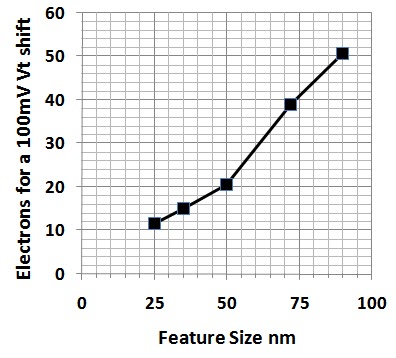
They also illustrated that at the 25-nm node, we’re down to about ten electrons on the floating gate for a 100 mV Vt shift, so in a typical MLC cell with 300 – 500 mV separation between levels, that’s about 30 – 50 electrons difference. With this degree of sensitivity, any traps in the stack can affect the Vt, so considerable effort has been taken to minimize trapping and charge leakage.

Electrons required for a 100mV Vt shift vs. cell feature size. 
(Source: Micron/IEDM)

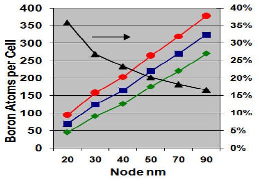
Micron also highlighted the sensitivity to boron concentration in the channel – instead of counting electrons, we’re counting atoms – at 25 nm we’re down to ~75 atoms, with a 3Ï?? variation of ~35%, and a corresponding effect on Vt; together with the increased sensitivity to noise at this node, some serious work has had to be done on the programming algorithms and error correction.


Number of Boron atoms per cell vs. feature size.
(Squares – mean; diamond – -3Ï??; circle – +3Ï??; triangles – ±3Ï?? percentage divided by the mean. Source: Micron/IEDM)

Later in the afternoon Macronix had a couple of papers (5.5, 5.6) on the other flash technology, charge trapping (CT) using a nitride layer. Macronix has been one of the more prolific industrial contributors in recent years, with six papers this year and seven last year.

Coincidentally, the first paper is on a BE-SONOS NAND flash structure (barrier-engineered SONOS), which uses a thin ONO layer under the charge-trapping nitride layer, instead of under the floating gate (as we speculate above, in the Samsung paper). The thin ONO layer is used as a “modulated tunneling barrier”, which suppresses hole tunneling at low electric fields for retention, but allows efficient tunneling at high fields for erase.

That gives us a ONONO stack under the gate;

Orthogonal Sections of Macronix 38-nm BE-SONOS NAND Flash
(Source: Macronix/IEDM)

The detail in the paper reveals that the lower two oxides are actually nitrided, and the ONO barrier layer thicknesses are 13/20/35 Å (bottom – top), covered by a ~70 Å nitride layer and another ~70 Å oxide, formed by oxidizing the nitride layer. 75-nm and 38-nm NAND flash structures were tested.

The intent of this work is to show that the reliability is improved by leaving the dielectric stack intact, as opposed to etching it when the gates are etched; previously it had been thought that the CT layer had to be etched to stop charge spreading on the nitride. In this they seem to have succeeded, since there is no change after a multiplicity of cycling tests, too many to go into detail here. The results indicate that there is no lateral charge spreading on the nitride CT layer.

Since the CT dielectrics do not need to be cut, this avoids any in-process damage at the edge of the dielectric; an advantage over the cut-dielectric version of CT-flash, but also over floating-gate flash, since these days the floating gate and STI are defined simultaneously, and the FG edge and tunnel dielectric are vulnerable.

The other Macronix paper (5.6) details a study of fast initial charge loss in CT-flash devices, incuding BE-SONOS, where the Vt shifts within a second of programming, and then saturates at a stable value. They minimised this by optimizing the film stack, and by refill programming to duplicate program levels.

Macronix has done a lot of work on the different CT-flash technologies, but BE-SONOS seems to be particularly pragmatic form, and a viable alternative to FG-flash – will we see it in production any time soon?

That was the end of day 1 of the conference; there were other papers that I missed, but I will be trying to review them in the next few weeks; meanwhile part 2 of IEDM retrospective will be up in a few days, covering the final two days of the meeting.