Earlier this month our faith in Panasonic was rewarded, and we found the chip! It took a few false starts buying Panasonic products that we tore down and threw away, but now we have a verified 32-nm, gate-first, high-k metal-gate (HKMG) product. The supply chain was a bit longer than we had hoped, but as promised the chip was shipped with a week 41 date code, in October.
So, for the curious, this is what a transistor looks like:
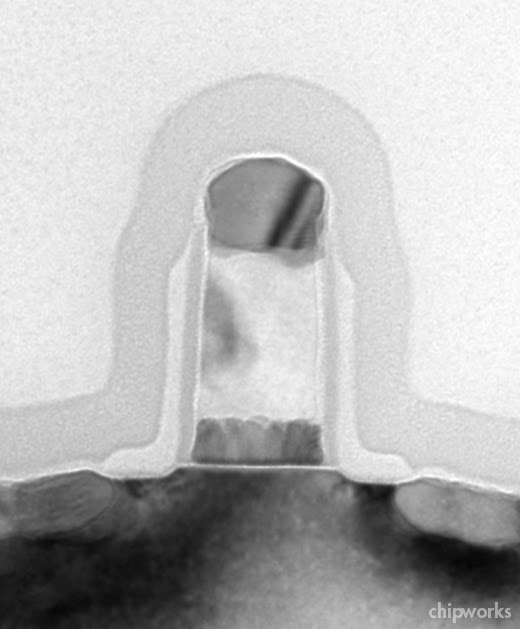 |
| Panasonic’s 32-nm HKMG NMOS Transistor |
We can see the TiN metal gate at the base of the polysilicon, and the thin line of high-k at the base of the TiN. Also noticeable are a dual-spacer technology (sometimes referred to as differential offset spacers), and a thin line of nitride over the source/drain extension regions (possibly indicating a nitrided oxide under the high-k). The salicide is the usual platinum-doped nickel silicide. Less visible are mechanisms of applying strain, other than the nitride layer over the gate; embedded SiGe and dual-stress liners are not used.
All of which is typical for Panasonic – their 45-nm product did not appear to use any enhanced strain techniques, and the only concession to PMOS enhancement was wafer rotation to give a 1-0-0 channel direction. The emphasis is different from Intel; rather than raw performance, the targets are increased integration, die size reduction/reduced cost, and now we have high-k, reduced leakage/lower power. The September press release does say that transistor performance is improved by 40%, but it also claims 40% power reduction and a 30% smaller footprint.
Here’s a 45-nm transistor for comparison:
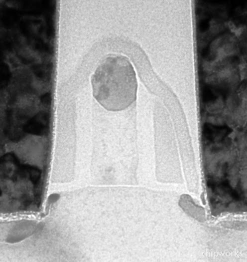 |
| Panasonic’s 45-nm Generation Transistor |
And, for good measure, Intel’s 32-nm device:
 |
| Intel 32-nm NMOS Transistor |
The part itself uses a nine-metal (eight Cu, one Al) stack with a hybrid low-k/extra-low-k stack. Die size is ~45 mm2 in a conventional FC-BGA package. Minimum metal pitch is specified as 120 nm [1], and we have found 125 nm in our early investigations.
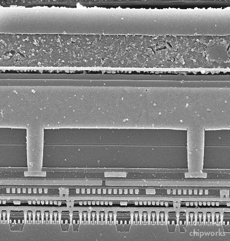 |
| Panasonic 32 nm General Structure |
Analysis is ongoing – stay tuned for more details, and of course we’ll be doing reports!
[1]S. Matsumoto et al., “Highly Manufacturable ELK Integration Technology with Metal Hard Mask Process for High Performance 32nm-node Interconnect and Beyond”, IITC 2010
