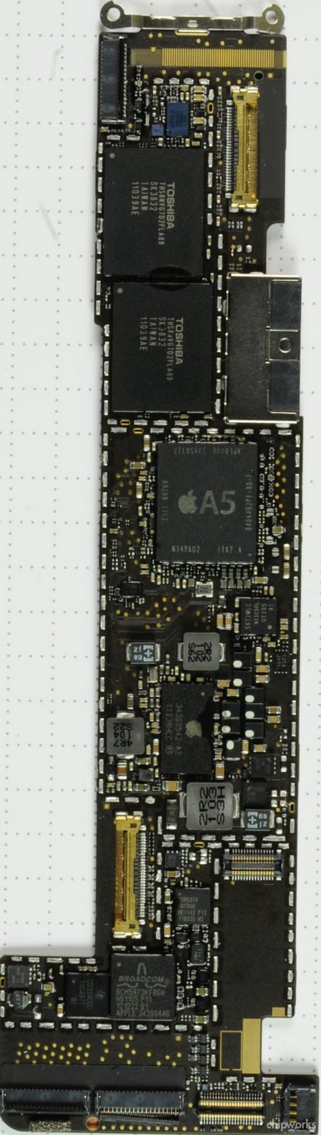
Forty-eight hours ago we obtained an iPad 2 and brought it back to the lab, and took it apart to have a look at Apple’s A5 processor chip. We’ve come to the conclusion that the main innovation in the new iPad is the A5 chip. Flash memory is flash memory (multi-sourced from Samsung and Toshiba in the iPads we’ve seen), the DRAM in the A5 package is 512 MB instead of 256 MB, and the touchscreen control uses the same trio of chips as the iPad 1 – not even a single chip solution as we’ve seen in the later iPhones. And the 3G version uses the same chipset as the Verizon iPhone launched a few weeks ago. This is the mother-board from a 32-GB WiFi-only iPad 2:
 |
| Motherboard from 32-GB iPad 2 |


The A5 can be seen in the centre of the board. If we look at the package we can identify the Apple’s APL0498 marking for the A5 (the A4 is APL0398), and also 4 Gb of Elpida mobile DRAM. Date codes are 1107 for the A5 and 1103 for the memory – only a few weeks in the supply chain here!
 |
| Apple A5 from iPad 2 |
The x-ray images show us that we have the usual package-on-package (PoP) structure, with two memory chips in the top part of the PoP, and the APL0498 processor on the lower half.
 |
| X-Ray Image of A5 Package-on-Package |
The two rows of dense black dots on the outside of the image are the solder balls from the memory chips in the top half of the package (connecting with the bottom half), and the less dense dots are the solder balls on the bottom half of the package connecting the A5 chip to the iPad board below. If you squint really hard you can see smaller dots about five rows in from the edge which are the flip-chip solder balls on the A5 die – and they take up quite a large proportion of the area, showing that this is a good-sized die.
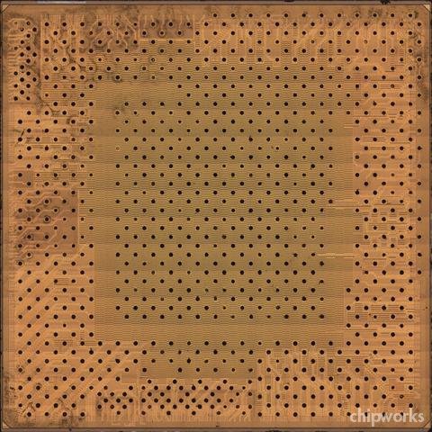
The die photo and die mark are shown here:
 |
| Die Photo of Apple’s A5 Chip from the iPad 2 |
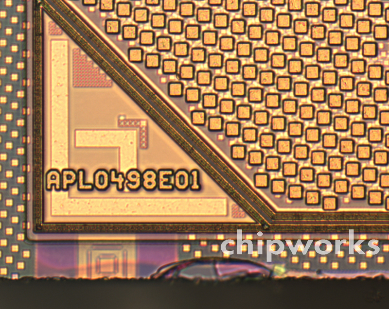
 |
| APL0498E01 Die Mark of Apple A5 Chip |
The x-ray is right – the A5 die is more than twice as large as the A4, at 10.1 x 12.1 mm (122.2 mm2), vs 7.3 x 7.3 mm (53.3 mm2) – here’s the A4 chip for comparison:
 |
| Apple A4 Die Photo |
Given that the A5 is a dual-ARM core, and has more graphics capability than the A4, more than doubling the size is to be expected, but it’s also a clue that this is still made in 45-nm technology.
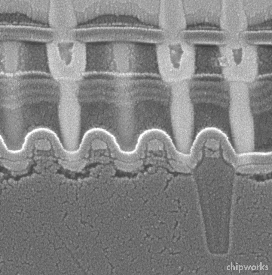
So after the web speculation that TSMC might be fabbing the A5 rather than Samsung, we had to take a look, and the quickest way is to do a cross-section and compare it with the A4 from last year’s iPad.
So here’s the A5:
 |
| SEM Cross-Section of Apple A5 |
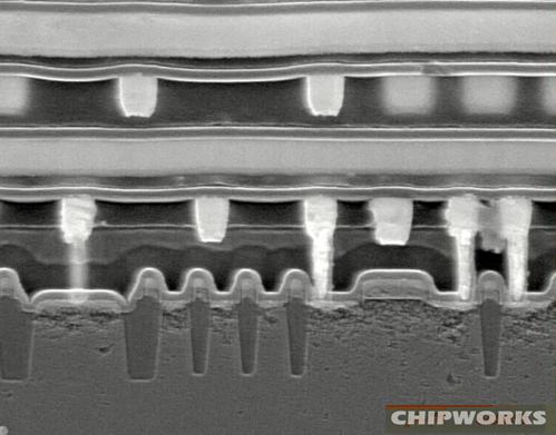
It’s a nine-metal layer part, with eight levels of copper and one aluminum. Zooming into the transistor level:
 |
| SEM Cross-Section of Transistors and M1 in A5 Processor |
And now the A4:
 |
| SEM Cross-Section of Transistors and M1 – M4 in A4 Processor |
At this scale even electron microscopes start to run out of steam, so not the clearest of images in either case, but good enough to see the similar shape of the transistor gates and the dielectric layers. So at least this sample of the A5 is fabbed by Samsung, just as all Apple’s processor chips have been for the last while.
Many thanks to the guys in the lab who’ve worked through the weekend to get this information – Chipworks is not really in the media business, but there’s always a buzz when a hot new consumer part comes out.
And on a different note, commiserations and condolences to our Japanese colleagues, they have much more important things of concern than the details of the iPad 2.