Insights From Leading Edge

Yearly Archives: 2011

IFTLE 81: GIT @ GIT, Part 2

Continuing our coverage of the 2011 Global Interposer Conference at Georgia Tech:


Jerome Baron — Yole Développment

Baron reviewed the status of interposer applications, markets, players and costs. Several of the following speakers would tout the potential of glass as an interposer substrate material due to its perceived lower cost position, outstanding Rf performance, and its ability to be fabricated in large format. Baron compared and contrasted glass and silicon based interposers in the chart below. Henry Utsunomiya, president of Interconnect Technologies Inc., later predicted that glass interposers would be used for FC — CPU and GPU starting in 2013.

Glass producers in the audience such as Corning Glass and Asahi Glass indicated that they were actively pursuing glass interposer technology as part of the GaTech consortium program. Christian Nopper, R&D director of ST Micro-Tours, indicated that glass substrates are already being used for their Rf IPADS technology [Integrated Passive and Active Devices].

Yole concluded that panel size processing will be mandatory for 2.5D interposers to be broadly adopted in the packaging landscape.


Rao Tummala — GaTech

Rao Tummala, founding director of the GIT Packaging Research Center, laid out the case for the GIT Interposer consortium. They are studying both silicon and glass interposers and view their low-cost large-panel size solutions as eventual replacements for the BGA packages currently supporting the interposer and chips. Their low-cost silicon solution is linked to the use of polysilicon vs. crystalline Si wafers.

In his presentation on the electrical issues of interposers, GIT’s Madhaven Swaminathan pointed out that glass has lower insertion loss and a higher level of insulation than CMOS grade silicon, but glass has return path discontinuities so the insertion loss can be much higher than silicon. Looking at eye diagrams for glass and silicon, they actually concluded that silicon is the best.

Swaminathan concludes:

Si interposer
– Insertion loss is higher, but there are workarounds;
– Crosstalk can be a killer;
– Better thermal performance spreads the heat and reduces cross talk;
– Better power delivery

Glass interposer
– Insertion loss is low;
– Crosstalk is low;
– Localized heating is a problem;
– Power delivery could be challenging

Nanhoom Kim of Xilinx pointed out that there are several physical limitations imposed on the interposer due to cost, manufacturability, and reliability.

Kim also showed that when it comes to electrical performance, thicker oxide, shorter TSV, and smaller diameter are better.

Choon Lee, head of corporate technology for Amkor, reminded us that all DRAM is not equal. 4Gb DRAM DIMM for servers costs ~$250 whereas 4Gb DRAM for a PC is ~$20 — quite a difference. It’s clear why stacked memory is first headed for server applications!

Kai Zoschchke from Fraunhofer IZM provided this convenient plot of TSV resistance vs. aspect ratio:

For all the latest on 3DIC and advanced packaging stay linked to IFTLE……….

Last week to enter the IFTLE contest! See IFTLE #78 for details.

Next week: Update on 3D activities at the 2011 IEEE IEDM.

IFTLE 80: GIT @ GIT

The inaugural Global Interposer Technology Workshop (GIT) was recently held on the campus of GIT (Georgia Institute of Technology). While we usually report on conferences based on numbers of attendees and presentations, Karen May, GaTech coordinator of the conference, had a much more interesting measuring stick — reporting that the 138 attendees consumed 106 gallons of coffee, 83 pounds of pasta, and 12 dozen ice cream sandwiches. Over the next few blogs I will try to update you on what was presented and what was said. Several of the presenters (it will be obvious which ones) did not want their slides released, so in those instances I will be going from my handwritten notes.

While every conference even remotely linked to microelectronics feels pressure to have at least one session dealing with 3D integration, this workshop was started, and appears to be unique, in that it’s focus is solely on 2.5D i.e. interposers.

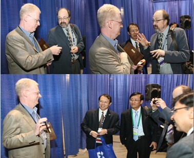
Row 2 (L-R): Swaminathan (GIT), Nopper (ST Micro), Sukumaran (GIT), Franzon (NC State), Huemoeller (Amkor), Matthias (EVG), Salmon (Semi), Kumbhat (GIT), Dunne (TI) ; Row 1 (L-R): Kitaoka (AGC), Ramalingam (Xilinx), Garrou (Assist Chair), Tummala (Chair), Dunne (TI)


Suresh Ramalingam — Xilinx

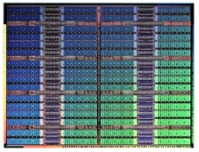
Certainly the highlight of the conference was Xilinx due to their highly publicized announcements on their Virtex 7 2000T FPGA, which uses a 21mm x 26 mm TSV interposer, which they have been sampling since September, and will have in full production in 2012. For details on the previous Xilinx announcements see [IFTLE 73, "Xilinx shows 2.5D Virtex 7 at IMAPS 2011" and IFTLE 23, "Xilinx 28nm multidie FPGA…"]. TSMC is fabricating the chip and the interposer, Amkor is bumping the chip and assembling the FPGA slices on the interposer, and Ibiden is fabricating the package substrate. Ramalingam emphasized that the interposer solution was necessary (vs. full 3D stacking) to insure proper thermal performance.

Increasing demand for FPGA capacity is reportedly coming from:

– Wired communications
– Image and video processing
– ASIC prototyping, emulation and replacement

All applications are constrained by the devices overall power budget and thermal concerns.

Full reliability qualifications are almost complete.

Future products are expected to be heterogeneous combinations such as the FPGA slices + SERDES chips shown below.

Doug Yu — TSMC

If the highlight was Xilinx, then the headline was TSMC, which concerning 3D and 2.5D has been very careful about what they say and how they are saying it — thus the comments made by Yu at this meeting drew great attention. Yu, Sr Director of Integrated Interconnects and Packaging at TSMC had some significant comments on 2.5D interposer supply chain developments. While there have been many recent proposals for how module fabrication tasks would be divided between foundries, IDMs, OSATs, and possible 3rd-party interposer suppliers, Yu proposed that for now, the interposers should be built completely by one party to define clear ownership and an efficient route to cost and yield improvements. Yu proposes that the foundries which can leverage their Cu processing capability, offer no customer competition (vs. IDMs), and have the design support capabilities would be the natural source for interposers. Furthermore, at several points during the two-day meeting, Yu reiterated that this is TSMC’s plan. However, you should also know that rumors in the audience indicate that TSMC is currently only engaging selected 1st-tier customers with their interposer technology, which should be no surprise. When asked when TSMC would be releasing their 2.5D ground rules, Yu indicated that TSMC does not release their ground rules for any of their processes except to their partner/customers.

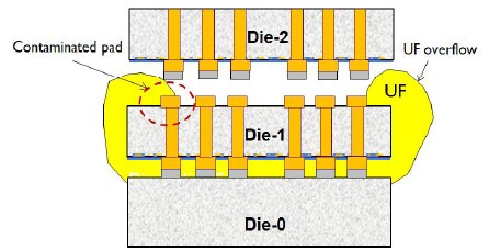
While everyone knows that TSMC is engaged with Xilinx on bringing their FPGA product to commercialization, it was of great interest to see Yu commenting that they were also working on mixed-chip solutions (like the memory + logic depicted below ) using interposers with 10um x 100um TSV).


Bryan Black — AMD

Byran Black, CTO of AMD, indicated that AMD is taking a "very broad view of TSV and stacking" and that the industry "will stagnate if we don’t get 3D." While Black claims that AMD has been involved in 3D for more than five years, he added that they are "intentionally not talking about what we’re doing."

Most of us remember Black from his days at Intel. In the early 2000’s he was already publishing seminal 3D papers including "3D Processing Technology and Its Impact on iA32 Microprocessors" [Proc. IEEE Int. Conf. on Computer Design, pages 316-318, 2004]

IFTLE should note that a similar "stealth" approach was taken by Micron until its recent announcements concerning its memory cube technology — see IFTLE 74, "HMC — TheMemory Cube consortium."

The audience certainly took notice when Black stated that the "Southbridge" was probably the last AMD chip that would be impacted by scaling. He envisions that in the future chip companies will be focusing process node development on specific application functionalities. He contends this will reduce mask layers and run time and increase yield, while improving performance and reducing power requirements, area, and cost for each individual functionality. These separately fabricated functionalities would then be combined vertically and/or horizontally on an interposer to form the final circuit function.


Paul Franzon — NC State

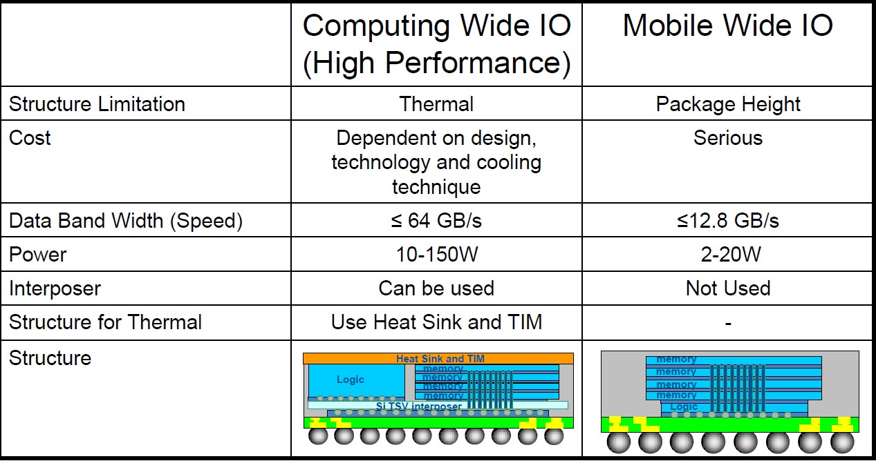
Paul Franzon, Professor of EE at NC State and long time 3D practitioner, compared the capabilities of SoC vs. 2.5D vs. 3D, agreeing that thermal performance was the outstanding feature of 2.5D as shown below. He reiterated, as many others have, that performance is often limited by memory capacity and bandwidth.

Franzon detailed the concept of "dark silicon" where most of the chip must be in "off mode" at any given time to meet predetermined power budgets. Low-power 2.5 and 3D solutions are expected to alleviate this situation.

Franzon also concluded that stacking processor on memory would allow the processor temperature to be better controlled by attachment to the capping heat sink, but would not offer enough temperature differential to the memory underneath the processor which is in intimate contact. This differential is much better when using an interposer. [See a similar discussion by LSI in IFTLE 77, "MEPTEC 2.5, 3D and beyond."]

We’ll finish up GIT @ GIT next week and then cover IEEE IEDM and RTI ASIP — plenty of important 3D news is coming your way in the next few weeks!

Also don’t forget to enter our IFTLE contest — see IFTLE 78 for details!

For all the latest in 3DIC and advanced packaging stay linked to IFTLE……….

IFTLE 79: Deca Technologies: Is there data to back the hype? Intel picks Franzon group to design 3D IC microprocessors

When I first started writing PFTLE and now IFTLE, I never thought I would be using Bill Maher to make a point in these technology-based blogs, since he and I are as diametrically opposed as two people can get when it comes to most political positions. But, as they say, "never say never." For those of you not familiar with him, Maher is what is known in the US as a TV celebrity, which means that he has done absolutely nothing other than express his opinions. Anyway, one segment of his show that I sometimes do agree with is called "New Rules" where he shows you something being done in everyday life that makes no sense and then proposes a new rule to fix the situation.

One of my long-time peeves is the announcement of some new "breakthrough technological advance" that does not tell me what they intend on doing or how they are intending to do it. So I am proposing an IFTLE "NEW RULE": If you’re not going to tell me how you are going to do it (for whatever reason), please contain the hype.

Recent headlines concerning a startup beginning operation included: "Disruptive Approach & IP Will Revolutionize Electronic Interconnect;" "Charting a new course for the future of electronic systems, Deca has launched a breakthrough approach to creating advanced electronic interconnect solutions;" and "We can take products from design to manufacturing in minutes rather than days." While others were content to copy these headlines and pass them on to you without question, IFTLE expects significant technical backup data to justify such statements — and thus we give our "Where’s the Beef" "award" [see IFTLE 3: Finding the beef and addressing 3DIC"] to the WLP startup Deca Technologies.

Going to their Web page for further information provides little help. The tab "Find out about Deca technologies" leads to this statement: "Deca’s vision of how technology and processes can be improved addresses many of the key challenges associated with advanced packaging technology, driven by a single goal of providing breakthrough products and services. Deca delivers tangible benefits through excellence in innovation, responsiveness, and production performance, resulting in: – Rapid new product introduction, – Industry leading cycle time, – Optimized ROI." Hummmmm…where’s the beef?

The site’s "How are we changing the game" tab leads to this: "The Deca ethos strives for exponential improvements across the board through a philosophy called ’10x thinking. Through Deca, traditional wafer fab batch-based processes are giving way to a novel high speed approach. Put simply, our ’10x thinking’ ethos delivers flexible technology that saves money, reduces cycle time, and expedites the introduction of new products to market." Double-hummmm…

So what do we know for sure?

1. Deca is entering the WLP market. That would have been news in the mid 1990’s, but this is now a maturing, although admittedly still-growing industry segment.

2. Deca believes that by using "non traditional equipment" they can lower the pricing on these products. Of course, with no further explaination of what that "nontraditional equipment" is or its unique use.

3. Deca is convinced that their turnaround time will be significantly less that that currently offered. I read that as ASE, Amkor and the other OSATs. IFTLE contends that one should not brag about this until they have developed a track record for doing it.

4. IFTLE likes factual, low-hype announcements with deep technical backup. But as Dennis Miller (another US TV celebrity) says "That’s just my opinion; I could be wrong."

IFTLE wishes Deca nothing but good fortune and looks forward to reporting on what their technology is and how it is progressing in the future, when that information is eventually made public. Until then: A little less hype and a little more information, please.

$1.5M Intel grant to NC State to design low-power processors

A $1.5 million grant from the Intel Corp. will be used by Paul Franzon, lead researcher and Professor of EE and Computer Engineering at NC State University, to develop a 3D CPU with 15% to 25% better energy utilization. In addition to Franzon, the research team includes Eric Rotenberg and Rhett Davis of NC State, and Krishnendu Chakrabarty PhD. of Duke University.

One problem the participants plan to address is "how to reconcile chips that are designed and manufactured in different places to different specifications so that they can work together in three dimensions. […] We will also address questions concerning heat dissipation." Franzon added that the goal is "at least a 15% improvement in performance per unit of power, through architectural and circuit advances."

They plan to have a prototype developed by 2014, and will also be addressing "test and yield" challenges — such as how manufacturers can test individual CPU components to ensure they are functional.

PFTLE/IFTLE Contest still underway

The contest involving naming key players in 3DIC and advanced packaging that have been discussed in the last several years by PFTLE/IFTLE is still ongoing and will be open to your guesses till December 31st.

See IFTLE 78 for rules and regulations and remember to send your guesses to pgarrou/[email protected] if you want to win the MRS 3DIC book prize. Good luck to all of you!

IFTLE 78 Beginning 5 Years of PFTLE / IFTLE

As I said a few weeks ago, we have now entered Year 5 of Perspectives from the Leading Edge (PFTLE [link], in the now deceased Semiconductor International) plus Insights from the Leading Edge (IFTLE) that you find here every week in Solid State Technology. Both of these are due to the trust that Pete Singer, editor-in-chief, showed in me five years ago.

When I started many said it would be impossible to get enough fresh material for a weekly technical blog in 3DIC and advanced packaging. I think we have proved the naysayers wrong! I have tried to fill these blogs with the data, because we are scientists and we want to see the data. I have not made an exact count, but I would bet that there have been more than 1000 figures that have come to you in the more than 200 blogs as we enter Year 5.

I said IFTLE 78 would be something special — and I am a man of my word. First, I will review two of the most entertaining stories of the year, stories that hopefully made you laugh and will yet again. Then we will have a contest: the winner of the contest will win a copy of MRS volume 970: "Enabling Technologies for 3D Integration" edited by Bower, Garrou, Ramm and Takahashi, still in shrink wrap (photo at left). The winner will be determined by whomever can identify the largest number of people (name and current affiliation) that you have seen previously on the pages of PFTLE/IFTLE.

This is a take-home quiz so you can go back to the old blogs and check — but do it quickly! The winner will be determined as whomever sends in their email response the soonest, based on arrival date and time, at the following email address: pgarrou/[email protected]. The contest officially ends on Dec. 31st, 2011. Only responses to that email will count — responses sent to my other email accounts will be disqualified. Employees of Pennwell, Microelectronics Consultants of NC, TechSearch International, Yole Développment, or Research Triangle Institute are disqualified (but can send in their guesses if they want to). The winner will be announced in early January 2012 along with a picture and short bio. Good luck to everyone!

Now for the two most entertaining stories of 2011…

The second most entertaining story can be found in IFTLE 47, "IBM 3D Cooling, TSMC Pkging, UMC 3D Equipment, the CIS Mkt Grows." This past spring at the Hanover Fair Germany, IBM CEO Sam Palmisano presented German Chancellor Merkel with a prototype of the IBM liquid cooling 3D chip stacking project developed at IBM Research-Zurich (see below). In front of the assembled audience and press, Merkel asked Palmisano: "Did you take this from Intel?" Quick on his feet, CEO Palmisano replied, "No, ours are better."

The Number One most entertaining story was reported in IFTLE 62 "Whats in a Name?" An EE Times article reporting on information released by the Taiwan External Trade Council quoted an "anonymous source" saying that "TSMC’s projected delivery of 3-D chips matches that of Intel, the world’s biggest chip maker". Only problem is that TSMC was talking about stacked 3D chips and Intel was talking about trigate transistors (i.e., finFETs). Nothing in the story made much sense since they were trying to compare apples to oranges — as many of the subsequent commenters pointed out.

Responses to this story by the EE Times readers were harsh:

"TSMC is referring to 3D interconnect structures using through silicon vias. This has been in existence for quite some time, at least in R&D. What intel has built is a 3d transistor. There is a lot of difference between the two. Kindly refrain from misleading people. This is wrong information. Please correct…"
"FINFET and TSV 3D are two completely different technologies. The report is confusion and misleading by comparing these 2 technologies…"
"I agree that this article is terribly misleading and really doesn’t make a lot of sense as it mixes apples with oranges. I don’t think the author is technically very well informed on this subject…"
" It’s a BS article – trying to make a connection to Intel Tri Gate is nonesense and misleading…"
"Dumb article. As others have said, Tri-Gate transistor technology is a totally different thing than TSV interconnect technology…"
"Beating Intel to 3D" by comparing TriGate to TSV is nonsensical…"
"Is eetimes becoming a tabloid? I am wondering about the credentials of the article writer!"
"I agree, what a pathetic article. I’m not an EE or even close to one, but even I know exactly how wrong and stupid this article is…"

WOW. We should note that EE Times offered an apology and correction shortly thereafter.

So, time for the contest… Below you will find the faces of 49 people whose stories have filled the pages of PFTLE/IFTLE over the years. Send in your guesses as to who they are and where they are employed — and you could win the prize! Good luck everyone, and thanks for your continued readership!

For all the latest in 3DIC and advanced packaging stay linked to IFTLE……….

IFTLE 77: MEPTEC 2.5, 3D and beyond

Last week in Silicon Valley MEPTEC and Semi held the "2.5D, 3D and Beyond Bringing 3D Integration to the Packaging Mainstream" Conference.

Zeki Celik, principal engineer in the package design and characterization group at LSI, looked at the thermal characterization of various 2.5 and 3D package configurations. Option 3, where the logic die is not heat sinked to the lid, results in the overall highest TJ, max. Option 2, where the silicon interposer is between the memory and the logic die, can be heat sinked to the lid lowers the overall temperature, but equilibrates the temperature of the memory to the temp of the logic. Option 1, which is the silicon MCM-D option, is the overall best solution with the lowest memory temperature.

Marnie Mattei, senior director of TSV product development at Amkor Technology, examined assembly strategies for interposed products. Primary drivers for interposers, which are now pretty much stansdardized at 100μm thick, are shown below.

Product challenges include:

Die-die / Die-substrate joining
– Micro bump uniformity; method of join; materials

Die-die X-Y spacing
– Fillet sizes and pad metallurgy
– Process assy sequence; micro-join method & materials

Thermal / power management
– Use of lids, stiffeners & passives
– Underfill/resin bleed, adhesive compatibility
– Process assy sequence; micro-join method & materials

Warpage control
– Interposer warpage; substrate warpage
– Top die warpage — top die area density/distribution

Intermediate e-test points
– Process assembly sequence

Available assembly flows in Amkor include:

[tc=thermocompression, NCP=non conductive paste (preapplied underfill); CUF capillary underfill]

Sunil Patel, director of GlobalFoundries’ customer package technology group, looked at backside integration and global supply chain challenges for 2.5 and 3D. He sees some application segregation as follows:

GF’s perspective on supply chain options mimics many others, namely foundry-centric, OSAT-centric, and 3rd party-centric.

Although GF pointed towards many collaborations with customers, OSATs and institutes, no indication was given as to when and how to expect GF to begin volume manufacturing of 2.5 or 3D products. While others have recently proposed that GF manufacturing is imminent, IFTLE does not see this happening just yet; they are probably still a year or two away.

Subramanian S. Iyer is an IBM Fellow and chief technologist at the microelectronics division within IBM Systems & Technology Group, responsible for technology strategy and competitiveness, and functionally for embedded memory and three-dimensional integration. His presentation focused on prospects for 2.5 & 3D integration. Among his main messages:

– Scaling is getting more difficult and expensive and yielding less;
– Bandwidth and latency are at a premium;
– Power management, delivery, distribution, and dissipation are significant;
– Integrating large amounts of low latency memory is a major challenge for modern multi-core processor design;
– 3D achieves high performance and low power (AC); and
– Supply chain management will be the toughest nut to crack

Repeating a theme that Subu has shared at previous conferences, he showed the cross-section of an 11-level-metal, 32nm chip (below) to make the point that due to size miss match, sometimes vias-middle TSV must be connected at upper levels of metal and not at the lowest level as we usually draw them in our cartoons.

For all the latest in 3DIC and advanced packaging stay linked to IFTLE………………….

IFTLE 76: Advanced Packaging at IMAPS 2011, recent 3D announcements

Finishing off our look at IMAPS 2011, we will examine some of the advanced packaging presentations.

Materials

PDMS stamps have found a lot of use recently as stamps for soft lithography. NuSil, maker of high purity silicones gave an interesting presentation on PDMS (polydimethylsiloxane). Evidently there are impurities in the PDMS that must be removed to produce a low outgassing product (required for space use), and fillers can be added to adjust its natural mechanical properties.

Specialty Coating Systems gave a presentation on their Parylene (xylylene polymers) CVD polymer product line which can be used as chemically inert barrier layers. Of special interest were the properties of Parylene HT which shows resistance toward thermal and or oxidative degredation up to 450°C and its UV resistance makes it a candidate for use as a protective layer for LED devices.

Daetec has looked at PBI (polybenzimidazole) as a temporary bonding material due to its properties of high thermal resistance, low outgassing and low stress.

Freescale reported on the adhesion of molding compound to SiN and SiON passivation surfaces. Both passivation surfaces were treated with O2/Ar plasma prior to the molding process. It is found that the SiN surface performed better than SiON electrically without showing any delamination for the mold compound studied. Both passivation surfaces were analyzed by TOF-SIMS immediately before and after the pre mold plasma treatment. The major observed difference was in OH group intensity. OH is increased on the SiN surface after plasma treatment while it is decreased on the SiON surface after treatment. It is inferred that the presence of OH group enhances the mold compound adhesion.


Kaist has studied the suppression of Kirkendall void formation in Sn/3.5Ag /Cu solder joints by pre-annealing. Pre annealing electroplated copper at 500-600°C for 2 hrs significantly suppresses Kirkendall void formation in the Sn-3.5Ag/Cu solder joints. Grain growth was observed as anneal time and temperature increased. SIMS analysis shows the annealed Copper films contained less C and S impurities.

Pac Tech has examined "Wafer level Solder Bumping and Flip Chip Assembly with Solder Balls Down to 30μm " [PDF link]. They have examined placing solderballs by both WLSST (Wafer Level Solder Sphere Transfer) shown below and SB2 (solder sphere jetting)

For WLSST 40μm solder balls were successfully placed while balls < 40μm were not — because such placement requires a stencil with 15μm openings and no stencil manufacturers can deliver such a stencil today.

Solder jetting with 30μm SnAg3Cu0.5 solder balls was successful, although such small balls of other solder compositions were difficult to obtain from suppliers. Underfill processes for flip chips with 30μm and 40μm solderballs were developed. Reliability was tested according to MIL 883G — 8000 temp cycles between -55 and +125°C were passed.

Recent announcements in the 3D infrastructure

EV Group, IZM-ASSID JDA to develop chip-to-wafer temporary bonding

Upgrading 3D wafer level technologies to 300mm wafer size is the next step in effectively assisting leading companies in meeting the requirements of their future products. The ASSID (All Silicon System Integration Dresden), part of the Fraunhofer IZM Berlin, was established to meet this specific challenge. [see PFTLE 74: "All Silicon System Integration Dresden (ASSID) — A 300mm 3D IC line for Germany"]

As part of this program, ASSID and EVG have announced an agreement to jointly develop high-volume temporary bonding and debonding processes to support chip-to-wafer bonding manufacturing processes for 3D IC integration applications. The joint-development project will take place in ASSID’s facility in Dresden. Process development work will be accomplished using EVG850 TB/DB systems already installed at Fraunhofer IZM-ASSID’s facility.

Brewer Science and EV Group come to agreement on ZoneBOND

The recent announcement by Brewer Science and EVG [see: Brewer Science, EVG commercialize temporary wafer bonding with zoning laws] means the IP issues between the two parties have been settled and the technology can move forward. ZoneBOND defines two distinctive zones on the carrier wafer surface with strong adhesion in the perimeter (edge zone) and minimal adhesion in the center zone. Therefore, only low separation force is required for carrier separation once the polymeric edge adhesive has been removed by solvent dissolution or other means. [see IFTLE 61: "Suss 3D Workshop at Semicon West"]

Numerous major players were intrigued by the technology but have been awaiting this resolution before they move forward.

In a linked announcement, EVG announced temporary bonding /debonding) equipment modules that support ZoneBOND technology [link]. It is interesting that EVG has opened its equipment platform to "enable the use of a wide range of adhesives from various suppliers to give customers the most flexible choice of bonding materials." This can be interpreted as meaning that they are no longer as closely wed to the Brewer product line as they once were, a position previously adopted by their competitor Suss Microtec.

Invensas aquires Allvia patent portfolio

Invensas, a wholly owned subsidiary of Tessera, has acquired the patent portfolio of Allvia and agreed to a two-year collaborative partnership to "further develop technology and IP in the 3D space".

The 64 patent portfolio consists mainly of technologies and processing dealing with "silicon interposers, TSV and micro bumping for wide IO mobile and 3DS DRAM."

While it certainly makes sense for Allvia to turn over the IP side of its business to Invensas and focus on foundry manufacturing for customers (including Invensas), it is certainly interesting that Invensas, whose stated corporate goals are to "acquire, develop and monetize strategic intellectual property" agreed to Allvia retaining a "back license" to offer the IP to other customers as was reported [link].

IFTLE interprets those comments as meaning they are offering the products, not licenses to the IP, but we may be wrong.

For all the latest in 3D IC and advanced packaging stay linked to IFTLE……….

Hope to see many of you at the RTI ASIP [ Architectures for Semiconductor Integration and Packaging] Dec 12-14!

IFTLE 75: LED market is about to explode

IFTLE 75 is a nice round number and if we combine these with their predecessor PFTLE (still accessible here) we are now past 200 and approaching four full years of these weekly updates. Certainly no other information source available has been following 3D IC on a weekly basis for as long. I’ll try to come up with something special for IFTLE 81, which would be the beginning of Year Five.

Once again I thank all of you, my readership, for paying attention. Hopefully there continues to be something for each of you to learn from each and every blog.

We’ve spent a lot of time the last four years discussing what’s going on in the 3D IC space because undergoing this evolution some day will be viewed as a very important event in IC packaging history. But that doesn’t mean that there are no other very significant packaging evolutions and market opportunities going on at the same time. Certainly the LED space is one of those.

We all know that LED producers are looking at white light and replacement of the incandescent bulb as the "big dog" driver application in this space, and I have ranted on the demise of "Lester the Lightbulb" [see IFTLE 63: "Bidding Adieu to Lester Lightbulb"].

Yole Développement and IC Insights have both released recently some very interesting LED component and packaging market data. The overall LED marketplace according to Yole looks something like this:

Further, Yole’s LED experts expect all phases of LED production, including packaging, to undergo a >10Ã?? cost reduction over the next 10 years.

It is an IFTLE perception that backlighting for TVs will be equally, if not more important than home lighting.

LED-backlit TVs and smart televisions which allow consumers to browse and view shows directly from the Internet, have replaced 3D TV as the "must-have" features driving television purchases in 2011, according to the soon-to-be-released 2012 edition of IC Insights’ Integrated Circuit Market Drivers report. In 2011, LED-backlit TVs are expected to account for an estimated 37% of global TV shipments, up from 15% in 2010. IC Insights forecasts that LED TVs will represent 53% of digital TV shipments in 2012. [see LED TV, Smart TVs Drive Digital TV Units in 2011 as 3D TV Wanes]

Besides being thinner and lighter, LED-backlit TVs have rapidly gained favor among consumers because they tend to offer broader color range, improved contrast ratios, and use less power. Also, LED TVs are said to be more reliable, offering over 100,000 hours of life compared to traditional cold cathode fluorescent lamp (CCFL) LCD TVs, which are often rated at 20,000 hours. [Although I do wonder how they tested this — see "Lester the Lightbulb" discussions.]

In general, digital TV growth rates are expected to remain fairly flat in developed markets (e.g., North America, Europe, and Japan) through the forecast period, since the big upgrade cycle in these regions has mostly already occurred. However, India, China and other countries throughout the Asia-Pacific and Latin America are forecast to enjoy strong DTV growth. Fast-growth economies, increased disposable incomes, and large populations will drive this expansion. Asia-Pacific is undergoing a digital TV boom that some believe will result in 70% of homes having a DTV in 2015, up from approximately 35% in 2010.

That IC Insights report also notes how the method of delivering programming is quickly transforming broadcast television. Just as smartphones brought the Internet and thousands of applications to cellphone users, "smart TVs" are bringing Internet and Web 2.0 features to television sets and offering access to TV broadcasts, videos, movies, photos, and other content via the Web. An estimated 20% of television shipments in 2011 were smart TVs, but this is expected to increase to nearly 40% of in 2012. Consumers will be able to watch almost anything found on a Web site on their television.

While the leading edge of LED packaging is going wafer-level (see below) using bumping and backside TSV technology, the bulk of the packaging as it enters the backlighting market is still on lead frames as shown below for the Osram Golden Dragon. Package development for LEDs appears to be in its infancy similar to where bumped WLP devices were a decade ago. Expect to see rapid changes in LED packaging over the next five years.

For all the latest in 3D IC and advanced packaging, stay linked to IFTLE……….

IFTLE 74 The Micron Memory Cube consortium

Most of you by now have seen the announcement that Micron has joined with Samsung to create the "Hybrid Memory Cube (HMC) Consortium" with fellow founding members Altera, Open Silicon, and Xilinx. [link 1, link 2]

The consortium is built around Micron’s hybrid (previously referred to as "hyper") memory cube technology. The initial goal of the consortium is to define specifications for HMC. The HMC interface is totally different, having nothing in common with current DDR implementations, so it is felt that standardization and adoption by major producers and users is the only way that HMC will become a standard memory product for the industry.

We have previously addressed the fact that the memory bandwidth required by high-performance computers and next-generation networking equipment has increased beyond what conventional memory architectures can provide. The term "memory wall" has been used to describe the problem. A solution to the memory wall problem requires an architecture that can deliver increased density and bandwidth at significantly reduced power consumption.

Micron initially announced their memory breakthrough earlier this year [see IFTLE 38: "Of Memory Cubes and Ivy Bridges — More 3D and TSV"], and began releasing information at conferences this summer [see J.T. Pawlowski, "Hybrid Memory Cube: Breakthrough DRAM performance with a fundamentally re-architected DRAM subsystem", Proc. 23rd Hot Chips Symposium, 2011].

While DDR DRAMs have gotten bigger through the years by increasing the parallel arrays of DRAM cells on chip, they remain limited to the bandwidth supported by package I/O. DDR3-1333 and DDR3-1600 devices currently offer bandwidths of 10.66 Gbps and 12.8 Gbps respectfully. The HMC is a stack of multiple memory die sitting atop a logic controller chip bonded together using TSV. This greatly increases available DRAM bandwidth by leveraging the large number of I/O pins available through TSVs. Both the number of contacts and their shorter lengths enable dramatically higher data transfer rates than today’s memory other memory architectures — Micron has shown prototypes rated at 128 Gbps.

Current DRAM burns a huge amount of the power in laptops and phones. Brian M. Shirley, VP of DRAM solutions at Micron, claims that the company’s hybrid memory cube technology "offers a 20-fold performance increase while reducing the size of the chip and consuming about one-tenth of the power," while occupying 10% of the volume of a DDR3 memory module.

[Performance & Power consumption Paradigm shift due to HMC (left); TSV stacked memory layers on logic layer (right). Source: Micron]

Micron reports that the HMC module achieves and exceeds 128 Gbps by using parallel channels. An image of the first-generation Micron HMC memory die showing the large number of I/O coming off each die:

[HMC Memory Device showing large Number of I/O. Source: Steve Liebson, Cadence EDA360 Insider blog]

Joe Jeddeloh, whose Micron team developed the logic portion of the HMC has described [link] the key "themes" of their technology as follows: "Instead of a DRAM die being one large device that has one set of I/Os on it, we break it into, say, 16 separate DRAMs, in essence much like a multicore processor. Each of those DRAMs has its own interface so when you go to access data, you go to a very local area of DRAM […]It’s a more directed access." Then, "we move that down the Z direction on a TSV."

When asked about the impact of 3D stacking on memory performance, Jeddeloh responded:

"When you think of a DIMM, maybe it has 4, 8, 16 [memory cell] banks in it, …once you go to a memory cube where you have these tiles and partitions, each of those has its own bank structure. So instead of 8 banks, you have 128 banks, 256 banks and each of these are put into parallel DRAM structures so you have a tremendous amount of concurrency available. You can think of a many-core processor coming at a many tiled memory system that marries up and can handle a lot of concurrent transactions."

In terms of mating this memory to today’s and future microprocessors, Jeddeloh commented that "As we go to more and more cores on processors [they become] more and more bandwidth-hungry. In this generation, you can’t stack the DRAM on top of the processor because the processor is too hot. That means the processor has to go off-chip to get that bandwidth [and] you need to connect a pipe to that processor that can bring in as much bandwidth at the lowest amount of power." Micron’s HMC technology, he explained, "can put more density in a very local area and put that right next to the processor." He also characterized power as the No. 1 theme going forward: "Once we reduce that power, we can create a smaller, more efficient I/O structure when the processor and the memory system are right next to each other. If you have, say, eight cubes hooked up to a processor, there’s a tremendous amount of bandwidth and concurrency that can happen in a very small area."

Concerning heat issues in the HMC, Jeddeloh noted that "DRAM doesn’t like heat; it messes up the refresh. If we are not on top of the processor, the heat is manageable. Once you create that low-power I/O […] and you’re not creating as much power within the cube itself, then you stack it up and pull the heat out the top."

[160 Gbps = 1 HMC or 15 DDR3-1333 DIMMS. Source: Micron Technology]

Scott Graham, general manager for Micron’s Hybrid Memory Cube (HMC), predicts that HMC impact will be seen in multiple markets such as high-performance computing, networking, video, medical, energy, wireless communications, transportation, security — basically any applications that will require the transfer of tremendous amounts of data. When asked about the Samsung partnership, he answered: "We need multiple sources for a broad adoption," since the industry is not comfortable with any sole source products. He indicated that the plan of record is to begin production in the second half of 2013.

At the recent Intel designer forum (IDF 2011) we found out that Micron teamed up with Intel to create the technology [link]. The company highlighted that a big impediment to scaling the performance of servers and data centers is the available bandwidth to memory:

"As the number of cores on a microprocessor increases, the need to feed the cores with more memory data expands proportionally. There [are] severe limitations to achieving high-speed and low-power using commodity DRAM […] We came to the conclusion that mating DRAM and a logic process based I/O buffer using 3D stacking could be the way to solve the dilemma. We found out that once we placed a multi-layer DRAM stack on top of a logic layer, we could solve another memory problem which limits the ability to efficiently transfer data from the DRAM memory cells to the corresponding I/O circuits."

Intel CTO Justin Rattner demonstrated the Hybrid Memory Cube toward the end of his keynote lecture which can be seen here [link]. Rattner noted that the HMC was "the world’s highest-bandwidth DRAM device with sustained transfer rates of 1 terabit per second (trillion bits per second). It is also the most energy efficient DRAM ever built."

It is currently unclear whether Intel holds any of this HMC IP — and it is equally unclear why Intel was not a founding member of the HMC consortium. IFTLE will follow this evolving story closely.

For all the latest in 3D IC and advanced packaging stay linked to IFTLE……….

IFTLE 73: Xilinx shows 2.5D Virtex 7 at IMAPS 2011

Xilinx 2.5D FPGAs

Liam Madden, corporate VP of Xilinx, gave the keynote presentation to kick off the 2011 IMAPS 44th Int. Symp. on Microelectronics a few weeks ago in Long Beach CA.
Last fall Xilinx announced a single layer, multi chip silicon interposer for its 28nm 7 series FPGAs. Looking at module assembly, first the four 28nm chiplets are mounted on a 25 �? 31 mm , 100μm thick, silicon interposer with 45μm pitch microbumps and 10μm TSV. The interposer is then assembled on a 35 �? 35mm BGA with 180μm pitch C4 bumps. The FPGA slices are connected by ~10,000 connections created on the silicon interposer. Compared to connections on a PWB, the interposer interconnect technology provides over 100�? the die-to-die connectivity bandwidth per watt, at one-fifth the latency.

Madden indicated that the use of an interposer (known as 2.5D) was the right choice for FPGAs since the "10,000 routing connections" if they would have been TSV in the FPGA slices, would have used up valuable chip area making the chips larger and more costly than they are now.

TSMC is fabricating the chip and the interposer and bumping the interposer, while Amkor is bumping the chip and doing the module assembly. Madden gladly showed one of the modules to the packed audience:

[Madden showing Virtex 7 module with James Lu ( RPI) and GS Kim (CEO of EPworks) looking on]

Madden indicated that the Virtex 7 HT will consist of 3 FPGA slices and two 28gbps SerDes chips on an interposer capable of operating at 2.8Tb/sec. In their paper "Advanced Thermal study of Very High Power TSV Interposer and Interconnects for 28nm Technology FPGA," Xilinx details the thermal study of TSV interposer technology for high performance 28nm logic die mounted on a silicon interposer with Cu-filled TSV. Based on DOE experimental results optimized TIM material, underfill, bump pitch and passive heat sinks were selected resulting in the following optimized thermal results at 55°C or 75°C ambient. Simulation results confirm that for the selected passive heat sink the high power FPGA package is thermally reliable and meets thermal specs.

Xilinx also reported on quality and reliability in their paper "Quality and Reliability of 3D Interposer and Fine Pitch Solder Micro-bumps for 28nm Technology." Microbump (FPGA to interposer) resistance was measured from Kelvin structure measurements.

Interposer stress and delamination risk were carefully studied through simulation and thermal cycling. Simulation results indicated that the overall stresses in the silicon, SiO2 insulator and copper via are below the fracture strength of the given materials.

During package level reliability testing, the 3 main factors evaluated were type of underfill, top die thickness and interposer cleaning . Test samples were exposed to level 5 preconditioning, HTOL (high temp operating life) and TC (temp cycling). Reliability results showed that higher Tg underfills passed all tests . Failures were observed with lower Tg underfills. In addition proper interposer cleaning and die thickness reduction were necessary to prevent delamination.

Wafer applied underfills for 3D

IMEC addressed the "Use of Wafer Applied Underfill for 3D Stacking." In the case of die-to-package UF one is looking to mitigate the CYE differences between the laminate package substrate, the ~100μm solder bumps, the silicon die, and the package overmolding — whereas in the case of die to die assembly such as 3D structures the underfill has to mitigate the CTE differences between the 2 silicon die and the ~ 10μm microbumps. Thus there are different requirements for the two.

In 3D packaging the main challenges for underfill are the narrow gaps between the chips and/or the chip and the substrate (~10μm) and the fine pitch between the bumps (i.e. 20μm). The use of capillary underfill (CUF) is time-consuming as requires excess space around the die for the dispense action. In the case of no flow underfill (NUF) the materials is dispensed on the substrate before the die stacking. Materials need to be transparent so you can see the alignment marks during the flip chip operation, dispense timing since this is still done for each individual die and underfill/filler entrapment between the bump and the pad.
For 3D, CUF is not an option due to the narrow gap and the fine bump pitch. NUF is a better choice but suffers from the transparency requirement and dispense volume control (i.e. excess underfill can be thicker than the bumps and thus hinder chip to chip bonding and/or squeezing out excess underfill can "backside overflow" (see pic below) which can contaminate backside pads.

Wafer applied underfill is considered a strong candidate for 3D because theoretically it can significantly increase throughput. It can be done by either spin coating or dry film lamination.

IMEC challenged 9 global underfill suppliers with the following criteria:

– Uniform material thickness ( < 30μm, target 10μm)
– Gap fill for <40μm bump pitch
– Transparent to allow alignment
– Tacky at ambient temp
– Low cure temp, usable up to 250°C

One spin coat and two dry film materials were submitted for testing. After initial testing IMEC was left with one spin on material and two dry films.

After fabrication of test vehicles IMEC daisy chain yields of 0% eliminated the "hybrid dry film" and resulted in 20%-50% yields for the remaining epoxy spin on and dry film. The latter two materials are being considered for further development.

3D activity at ITRI

John Lau and co-workers from ITRI gave several presentations on the various aspects of 3D IC that they are working on at ITRI, many of them tied to their 3DIC test vehicle. [ see IFTLE 52, "3D and Adv Pkging at ICEP 2011"]

In their paper "Oxide Liner, Barrier and Seed Layers and Cu Plating of Blind TSVs on 300 mm Wafers for 3D IC Integration" they focused on their process development for TSV filling. They use an AMAT PECVD to deposit TEOS SiO2. At 180°C deposition temperature they find that step coverage is improved by higher temp, higher Rf power, lower pressure, and lower TEOS flow.

For barrier layer and seed, a AMAT self ionized plasma PVD system is used for Ta barrier and Cu seed. They achieved < 50 pA leakage current between 10μm �? 60μm TSV. In their paper "Thin Wafer Handling of 300mm Wafers for 3D IC Integration" IRTI points out that if your dicing tape adhesive strength is "too strong" it may strip immersion gold off of the chip pads. In their presentation "Wafer bumping and Characterization of Fine Pitch Lead Free Solder Micro bumps on 300mm wafers for 3DIC integration" they offer that the difference in volume between FC solder balls and micro bumps is > 20�? and the smaller and thus IMC and Kirkendall void formation issues are more pronounced for the smaller bumps. For this reason ITRI does not reflow the micro bumps before joining and the micro bump assembly is usually fluxless to reduce the chance of entrapping flux during solder reflow. Underfills are more critical for micro bumps. UBM thickness is > 10�? less and the budget for undercutting the micro bumps is much smaller meaning that the process windows are smaller.

For all the latest on 3D IC and advanced packaging stay linked to IFTLE……….

We have previously reported that the IEEE International 3DIC Conference was moved from its initial October 2011 date outside Tokyo to Jan 31st 2012 in Osaka due to the unfortunate earthquake/tsunami events of this past year. The US program committee, which was scheduled to hold the 2012 even in San Francisco in October 2012, has decided to postpone their event till 2013 in deference to the unusual events surrounding the 2011 Japan meeting. We strongly recommend support of the coming meeting in Osaka.

IFTLE 72: 2011 IEEE 3D test workshop

For the second year the IEEE 3D Test workshop was held in conjunction with ITC (IEEE International Test Conference), with Yervant Zorian of Synopsys as general chair and Erik Jan Marinissen of IMEC as program chair. More than 125 attendees attended 11 sessions which covered all of the mainline test issues: Executive views (Synopsys, ASE, Samsung, Teradyne,Cascade, Cadence ect.); 3D electronic Design Automation (EDA); wafer probing; standardization; and challenges and solutions for wide IO DRAM stacking.

Unlike a few years ago where Universities were the main groups involved with developing 3D test protocols, the 3D Test workshop list of corporate sponsors now says all we need to say about the desire for the world’s major design and test houses being involved.

Eric Strid of Cascade Microtech looked at the status of probing:

Brandon Noia and Krishnendu Chakrabarty of Duke University looked at "Methodology for Pre-bond Test of TSVs and Breakpoints in High Performance 3D-SICs." If we assume the following is the accepted 3D Manufacturing/Test flow:

The goal is to detect TSV defects prior to bonding (pre-bond) but we are faced with:
— Pre-bond TSVs are single ended
— Current probe technology: Minimum pitch 35μm but TSVs will be â??¤5μm with pitch of â??¤10μm and densities of â??¥10,000/mm2

TSV test can be done by BIST (built-in self test) and DfT (design for test).

In a joint presentation between Cadence, IMEC and TSMC entitled Automation of DfT Insertion and Interconnect Test Generation for 3D Stacked ICs", Sergej Deutsch of Cadence concluded:

  • 3D test challenges include pre-bond and post-bond testing
  • 3D-DfT architecture
    — I/O wrap and test-only pads for pre-bond testing
    — Serial and parallel test access mechanisms
    — Test turns: to bypass upper dies in stack
    — Test elevator mode: for test paths to/from upper dies
    — DRAM top control interface
  • 3D wrapper insertion flow
    — Inserts 1500-style wrappers and 1149.1 for bottom die
    — Includes controls for I/O wrap and DRAM testing
    — Generates input to run ATPG
  • Industrial case study concludes: negligible area costs of 3D wrapper

Etienne Racine of Mentor Graphics gave a look at TSMC’s RF12 reference flow for die stacked on interposer.

For wide IO DRAM they offer the following:

Larry Smith from SEMATECH’s Standards group discussed the 3D Enablement Center, which was announced December 2010 by SEMATECH, SIA, and SRC. It is designed to meet SIA member needs in high performance, mobile, analog, mixed signal, MEMS, fabless, fablite, IDMs. Their mission: "Enable industry-wide ecosystem readiness for cost effective TSV-based 3D stacked IC solutions." Members include: ASE, Altera, ADI, LSI, NIST, ON Semi, Qualcomm, Hynix, CNSE, GlobalFoundries, Hewlett Packard, IBM, Intel, Samsung, TSMC, and UMC. Initial focus is on wide IO DRAM for mobile and high-performance applications:

Erik Jan Marinissen of IMEC updated the group on the status of IEEE P1838 the “3D-Test Standardization Study Group” chartered with defining the standards in 3D test and DfT. Their current project is P1838: “Standard for Test Access Architecture for Three-Dimensional Stacked Integrated Circuits”.

Focus:
— Generic test access to and between dies in a multi-die stack
— Prime focus on stacks with TSV-based interconnects

Test:
— Pre-bond, mid-bond (partial stack), post-bond (complete stack)
— Intra-die circuitry and inter-die interconnects
— Pre-packaging, post-packaging, board-level situations

Die-centric standard:
— Die-level features comprise a stack-level architecture
— Compliance to standard pertains to a die (not to the stack)
— Enables interoperability between die and stack maker(s)
— Standard does not address stack/product-level challenges/solutions (e.g. boundary scan for board-level interconnect testing)
— However, standard should not prohibit application thereof

Two standardized components:
— 3D test wrapper hardware per die
— Description + description language

Scan-based:
— Based on and works with digital scan-based test access

Leverage existing DfT wherever applicable/appropriate:
— Test access ports (such as IEEE 1149.x)
— On-die design-for-test (such as IEEE 1500)
— On-die design-for-debug (such as IEEE P1687)

Standard does not mandate:
— Specific defect or fault models
— Test generation methods
— Die-internal design-for-test

Further info can be obtained here: 3D-Test WG or here: Project P1838.

For all the latest on 3D IC integration and advanced packaging stay linked to IFTLE……….