Insights From Leading Edge

Monthly Archives: December 2012

IFTLE 128: RTI 3D ASIP Part 1; Lester the Lightbulb update

Every year since 2005 the 3DIC season as ended with the Research Triangle Institute-sponsored Architectures for Semiconductor Integration and Packaging Conference (which I coined ASIP several years ago as I became tired of typing out the whole phrase). This conference — with its totally invited agenda — gives us a good chance to look back at what has happened during the year.

This year the preconference symposium (which has turned into course-like updates of the most recent technological advances) consisted of myself, Erik Jan Marinissen covering test, and Minsuk Suh of Hynix looking at the key challenges for wide IO applications.

The keynote session consisted of Xilinx, Micron, Cadence, GlobalFoundries, and Ericsson giving us a look at 2.5/3D progress from their perspectives.
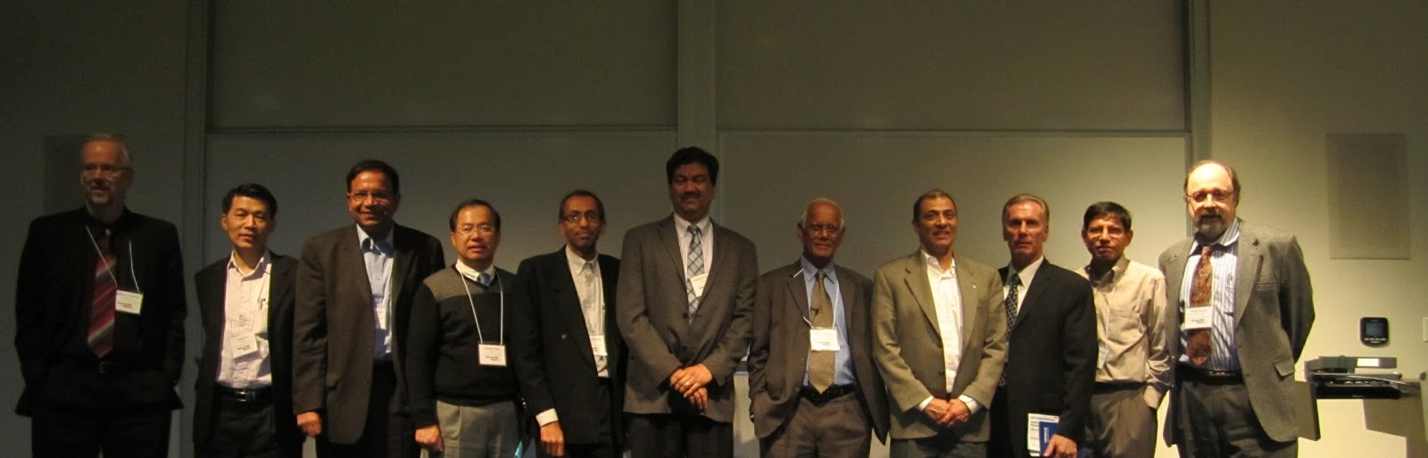
Keynote speakers (l to r): Vinod Kariat (Cadence), Tom Pawlowski (Micron), Carl Engbloom (Ericsson), Dave McCann (GlobalFoundries) and Liam Madden (Xilinx)
Micron
Micron chief technologist Tom Pawlowski discussed revolutionary trends in memory technology and the role of 3D. He noted that "node scaling is becoming more difficult bot for logic and memory…we are getting close to the end of the CMOS S curve…the future will be dominated by technologies that offer the lowest energy consumption, i.e. picojules/bit." While there are significant aspect ratio and materials challenges for 3-D NAND (vertical transistor tech not 3D stacking), NAND is in the process of transitioning to "3D in fab" technology since it relaxes lithography requirements
Most practitioners feel that DRAM technology will be replaced. Opinions range from "mid-2015" to "by end of 2019." New technologies that may be used include:


Pawlowski indicates that the Micron HMC 3D stacking technology [see IFTLE 74, "The Micron Memory cube Consortium" and IFTLE 95, "…Further Details on the Micron HMC…"] has in fact rearchitected memory and equalizes signal transit time in the x, y, and z directions.

Micron offered the following memory stacking roadmap:

Tezzaron

Longtime RTI 3D ASIP attendee Bob Patti has had a quite eventful year at memory startup Tezzaron. Late this year they announced thepurchase of the old Sematech facility in Austin (which was owned by failing SVTC) and the licensing of the Ziptronix direct bonding technologies ZiBondâ??¢ and DBI®.

The Austin facility will now be known as Novati technology which Patti referred to as "a production-style fab that can also do development." It gives Tezzaron the control of production capacity which is something they have yearned for, for many years.
Concerning the Ziptronix license Patti commented that "no one technology can do it all…this gives us superior performance in die to wafer." 

Patti reiterated several times that he would be an open platform and is working with e-silicon to get this to customers. Promising to become part of the "domestic supply chain" Patti now has a 300mm, ISO 9000, trusted fab which can build in 65 nm CMOS and has 6-7 interposer programs already underway.
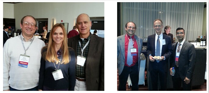
Tezzarons Bob Patti meets with (L) Kathy Cook and CEO Dan Donnabedian (Ziptronix) and (R) Matt Macray (RTI organizer) and Arif Rahman (Altera)
Lester the Lightbulb update
An engineer from the northeast who chooses not to reveal his name (political hacks now abound in the DOE and you certainly do not want to be called a non-believer!) sent an e-mail earlier in the month after he stumbled onto the IFTLE Lester articles. Here is his true story.
"…a couple of years ago I decided to put four LED PAR38 luminaires into my kitchen ceiling recessed cans. It took a couple of months for my wife to stop complaining about the harshness, but we eventually settled in and even got used to the half second startup time. Sadly, two of the luminaires failed within 18 months. Sylvania requires the original cash register receipt and UPC symbol, and most of us aren’t in the habit of saving such documentation on light bulbs. I’ve since rekindled my relationship with Lester."
Hmmmmm… methinks there are a lot more stories like this out there in the naked city [1950s US crime show humor].
By the way, several of these Lester articles have been picked up and retweeted and republished in the LED literature. Guess I won’t be invited to give the plenary lecture at any LED conferences, but that’s OK because I’m telling you the truth which is in short supply in some parts of the scientific community which have aligned with the politicos.

In my one-bulb, nonscientific test which we started in Aug 2011 [see IFTLE 63, "BiddingAdieu to Lester Lightbulb" ], recall the CFL burned out in less than a year [see IFTLE 109, "…Lester’s cousin CFL dies prematurely…"] but the LED and Lester are still both burning as of the end of 2012.  Lester has now exceeded his 1000 hr expected lifetime. BRAVO LESTER ! Lester sent along this message from San Quentin where he still remains on death row but is running out of appeals.


"When I replaced the candle many years ago there was a reason for that and I think I bettered mankind. The dudes trying to extinct me now are doing so with lies because they are greedy bureaucrats who are on the take. CFL and LED are not the cheapest solutions for your lighting needs and reduction of the country’s energy consumption would be better done in other ways"

"If you don’t exterminate me I promise to be obedient (just flip the switch and I’ll come running); honest (you’ll never find me trying to bribe you to buy me or lying about my qualifications); thrifty (hey, what else can you buy now a days for a quarter?, not my competitors, that’s for sure!); brave (I’m trying to keep my chin up as those evil lying Washington lobbyists are accusing me of ruining our country); and clean (when I do finally pass away simply put me in the garbage can and I won’t poison your babies if I happen to break on your floor)."

Thanks, Lester, for all you have done for all of us….
For all the latest in 3DIC and Advanced Packaging stay linked to IFTLE…….

IFTLE 127: Christmas wishes and thin wafer processing

First things first:

In a recent Yole webcast, Eric Mournier took a market look at thin wafer bonding and processing.

Wafer thinning is required in a number of high growth microelectronic areas.

Thin (< 100μm) and even ultra-thin semiconductor wafers (< 40μm) are in demand for:

— Reduced package thickness
— Better heat dissipation / thermal management
— Increased TSV density

This brings up issues since the thinned wafers are more vulnerable to stress and the dies can warp and break.

Yole sees the following wafer thinning roadmap:

By 2017 memory will dominate the thinned wafer application space:

The major players will be the expected memory "Big 3" of Samsung, Hynix, and Micron:

They see greater than 10M wafers going through temporary bonding in 2017, which would be approximately 8% of total thinned wafers. The power and 3DIC markets will drive temporary bonding on carrier.

This will result in a temporary bonder / debonder market of $250M in 2017.

For all the latest in 3DIC and advanced packaging in 2013, stay linked to IFTLE………….

IFTLE 126: 2012 GaTech Interposer Conference, part 2

Continuing our look at the 2nd annual GaTech 2.5D Interposer Conference (for part one, see IFTLE 125: 2012 GaTech Interposer Conference, part I):

Ahmer Syed of Amkor took a look at micro bump electromigration issues. Issues inherent to electromigration have been around a long time [see IFTLE 56, "Electromigration at the 2011 ECTC"]. It is known that current densities on 10K A/cm2 will induce EM within a few hours.

When we look at 2.5/3D we have radically changed the dimensions involved as shown below.

There is a 20�? increase in interconnect density from BGA to μbump and a 10�? reduction in pitch and ball diameter. Yet for the μbumps shown below they saw no failures even after 16K hrs of operation.

They conclude that:

– For WLCSP and BGA joints, they see Cu consumption and failure around the circumference

– For μbumps, they see copper conversion and IMC formation either during assembly or during current/temp stressing, but they see very long life

– While current carrying capacity for BGA and FC joints are in the expected range, μbumps can carry much higher current than theoretically predicted.

– Cu pillar bump interconnects provides the highest current carrying capability.

Nagesh Vordharalli of Altera quoted an IMEC study which shows that the sweet spot for maximum bandwidth will come from interposers with RDL lines/spaces ~3μm. Nagesh feels that silicon based interposers need to be in the 1-2 cents/ mm range to compete with future high density laminate technology.

Professor Joungho Kim of KAIST shared his assessment of Si vs. glass interposer electrical performance. Imajo developed comparative data for double sided interposers with 10μm TGV/TSV on 40μm and 100μm pitch. TSV had oxide insulator thickness of 0.5μm. He proposes that interposer type will depend on IO count and bandwidth requirements as shown below.

Nobu Imajo of AGC reported on their ongoing activities to develop low-cost, high-density glass interposers. AGC is looking at EN-A1 glass because of its better CTE match to silicon. They use an e discharge process to form the TGV. They are currently working with 60um TGV on 100μm pitch. Below we see 300μm thick glass with 60μm TGV (entry) and 40μm (exit).

They are working on metallizing the TGV with copper. For thinner substrate structures, a glass carrier will be required.

Representing Yole Développement, I reported that 2.5D/3D interposer revenues in 2017 is expected to reach $1.37B, or 15% of the packaging substrate market value.

By 2017 Yole expects silicon interposers to exceed the revenue of their glass counterparts by at least 3.5:1. During the panel session, I indicated that to me it is highly unlikely that we will see OSATS buying flat panel display lines to produce glass interposers. It is much more likely that we will see current flat-panel producers become aware of the potential market for glass interposers and enter the market themselves.

For all the latest on 3D IC and advanced packaging stay linked to IFTLE……………

IFTLE 125: 2012 GaTech Interposer Conference, part I

Many of the world’s 3D elite meet the 3rd week of November at the 2nd annual GaTech 2.5D Interposer Conference which focused on the technology and performance of silicon and glass interposers. Chairs Tummala and Garrou assembled an expert panel of many of todays fabricators and users to deliver keynote addresses and answer attendee questions on where we are and where we are going. This meeting is sponsored by IEEE CPMT, IMAPS, iNEMI, and SEMI.

Expert panel from left: Jon Greenwood (GloalFoundries); Doug Yu (TSMC); Sesh Ramaswami(Applied materials); Joungho Kim (KAIST); Suresh Ramalingham (Xilinx); Sitaram Arkalgud (SEMATECH); Rao Tummala (GaTech); Subu Iyer (IBM); Matt Nowak (Qualcomm); Nagesh Vodharalli (Altera); Phil Garrou (Microelectronic Consultants of NC)

Sitaram Arkalgud outlined SEMATECH’s comprehensive 2.5/3D program which includes:

They see bonding going through an evolution which leads towards thermal compression copper-copper bonding on a less than 30μm pitch. Arkalgud reported that current copper-copper bonding occurs at 400°C with a throughput of 0.5 wafers/hour. The SEMATECH goal is to develop a process that can improve on both of those criteria.

They claim to have demonstrated a low time / temperature process (245°C / 5 min) on patterned wafers and have a tool concept proposed which could increase wafer throughput to 30 WPH.

The current SEMATECH roadmap for copper-copper bonding and thin wafer handing is shown below.

Jon Greenwood of GlobalFoundries shared their thoughts on "collaboration" and how important this is for complex infrastructures like 2.5D or 3D. Since both UMC and GlobalFoundries appear to be behind TSMC in the introduction of a qualified 2.5D process [see IFTLE 122: TSMC officially ready for 2.5D, Apple order impact on TSMC] and they have both publically supported a collaboration approach vs. the TSMC "one-stop shopping approach, presenting arguments for this approach was not unexpected. Greenwood indicated that 3D is being focused in Fab 8 in NY while 2.5D solutions are being focused in Fab 7 in Singapore. Process development was done in conjunction with IMEC in Belgium and Fraunhoffer ASSID in Dresden. They specifically call out the Big 4 OSATS as their assembly partners.

Matt Nowak of Qualcomm, long an advocate 3D technology, reported that Qualcomm has now built "thousands of parts" and does not see anything stopping high-volume manufacturing (HVM) except cost.

Qualcomm defines high density for 2.5/3D as: 5-10μm TSV, AR ~ 10:1; 1K-10K TSV / μbumps; 10’s μm bump pitch. They see the following categories evolving:

Nowak indicates that Qualcomm will require a price of ~$2 for a 200 mm2 high-density silicon interposer. The high-density aspect is out of the reach of those proposing low-cost "coarse" interposer fabrication and the pricing appears significantly out of reach for the pricing structure for dual damascene foundry-based fine interposers.

For all the latest on 3D IC and advanced packaging, stay linked to IFTLE………………