Insights From Leading Edge

Yearly Archives: 2012

IFTLE 109 2012 IEEE VLSI Conference ; Lester’s cousin CFL Dies Prematurely

The  IEEE Symposium on VLSI Technology  is sponsored by the Electron Devices Society — ED and the  Solid-State Circuits Society — SSC. At this year’s conference, Micron gave further details on their hybrid memory Cube and TI detailed their studies on TSV induced stress on 28nm CMOS and Chuo Univ described a hybrid NAND + ReRAM SSD stack with better power consumption and product lifetime.

Hybrid SSD memory stack with ReRAM and TSV

Perofessor Takeuchi of Chuo Univ described a hybrid SSD architecture using ReRAM and high capacity NAND flash memory.

When SSDs are used for servers in financial institutions, performance is hindered and power consumption increased because random access is dominant. This causes data to get split up if the size of the data packets are not of the appropriate size (minimum for NAND is 16Kb). Takeuchi’s memory stack combines a NAND flash memory and ReRAM. ReRAM is used as both cache and storage memories. To overwrite a small amount of data in the NAND flash memory, software transfers the page of data to the ReRAM so that data is not fragmented in the NAND flash memory.

(Click on any of the images below to enlarge.)

A prototype, tested on an emulator, showed that compared with existing SSDs which only use NAND, the hybrid memory stack achieves an 11X higher data writing performance, 93% lower power consumption and 6.9 times longer product life. This assumed that the controller, ReRAM and NAND flash memory were connected by TSV. Although this has been hyped up by several reporters, we should note that it is possible to achieve almost the same results without using TSV. The major gain of using the TSV appears to be a 14% decrease in energy required to write as shown in the comparative table below.  

It is proposed that SSD in data centers would have to be changed out about 7 times less thus reducing expenses.

It should be noted that in order to use  the hybrid SSD architecture for different applications, it is necessary to change the controlling software algorithms.

Micron Hybrid Memory Cube (HMC)

We have previously discussed the fact that  Micron has created an industry group to collaborate on the implementation of an open interface specification for a new memory technology called the Hybrid Memory Cube (HMC). [http://www.hybridmemorycube.org/]

The HMC is a stack of multiple thinned memory die sitting atop a logic chip bonded together using TSV. This greatly increases available DRAM bandwidth by leveraging the large number of I/O pins available through TSVs. The HMC requires about 10% of the volume of a DDR3 memory module. It is claimed that the technology provides 15X the performance of a DDR3 module, uses 70% less energy per bit than DDR3 and uses 90% less space than today’s RDIMMs. [see IFTLE 95 "3DIC – Time Flies When You’re Having Fun; Further Details on theMicron HMC…"; IFTLE 74 "The Micron Memory Cube consortium"]

The HMC device uses TSV technology and fine pitch copper pillar interconnect.  The DRAM logic, responsible for DRAM sequencing, refresh, data routing and error correction is placed in a  separate high performance logic die.  DRAM and logic are connected by thousands of TSV. The DRAM is a slave to the logic layer timing control.  The HMC was constructed with 1866 TSVs on a roughly 60um pitch. 

HMC electrical performance is are compared to other DRAM modules below.

TI Studies Impact of TSV Stress on Electrical Performance

They found that the impact of TSVs on surrounding Si is tensile but that a tensile etch stop layer (ESL) counters the impact of the TSVs on near-surface Si where devices are present. Also, insertion of compressive shallow trench isolation (STI) between the TSV and device will also act to buffer this impact.
They conclude that "…the electrical properties of N/PFETs between 4 and 16um of TSVs are negligibly impacted (less than 2.3%)…" and that For Wide-IO Memory-Logic interface applications employing a 40 x 50 um JEDEC TSV array, ESD and decoupling capacitors which do not contain N/PFETs can be placed immediately adjacent to TSVs such that CMOS logic circuitry does not require placement less than 4 um.
CFL Fails While Incandescent Lester Still Going Strong

When last we discussed our hero Lester the incandescent lightbulb [ see  IFTLE 98 "Lester the Lightbulb vs CFL and LED: the Saga Continues"] we found out that an actual calculation of the cost of various electrical functions in my household revealed that lighting was responsible for $4.31 per month (that’s for operating 30 bulbs) on your electric bill and that saving three-quarters of that by using Lester’s lighting cousins CFL or LED would therefore save you about $36/year (if you replaced all 30 bulbs), which is not enough to buy you 1 LED bulb. The CFLs whose price was now down to about $4 each (vs $0.25 for Lester)  promised 9.1 years of lifetime (at 3 hrs use per day). Our test bulbs (CFL and LED) were installed on 08/15/2011 [ see IFTLE 63 "Bidding Adieu to Lester Lightbulb"]. So…cousin CFL lasted less than 11 months (vs the promised 9.1 years). I guess you’d have to call this an "outlier"?
So cousin CFL operated 11 months saving me 1/30 of $4.31 or 14 cents / month or $ 1.54 in 11 months â??¦but remember the bulb cost me $3.97 . You can do the math. And remember since the CFL’s contain mercury, I’m now supposed to contact the EPA for proper disposal instructions (yeah right !) 
Cousin CFL and cousin LED promised me "hope and change"…  "to transform US power consumption as we know it today." So far, I’m down $2.43 and need to replace the bulb. Typical Govt BS !
I guess we can understand now why the Govt. got involved to ban poor Lester from the shores of the US. Would anyone actually buy these CFL or LED bulbs, unless they were forced to ?
Cousin LED is still burning bright as are all the incandescants that were started at the same time. Be assured we will keep you up to date on cousin LEDs health !
For all the latest on 3DIC and advanced packaging stay linked to IFTLE………………………..

TI researchers have used NanoBeam Diffraction (NBD) to measure near-TSV Si strain in fully processed wafers. The electrical behavior of poly-SiON P/NFET transistors were characterized for full thickness wafers varying temperature, orientations and proximities to isolated and arrayed TSVs.
NanoBeam Diffraction measurements of Si strain within 5 um of TSVs were acquired for samples prepared from fully processed wafers, showing that for proximity greater than 1.5 um the impact of TSVs is negligible.

IFTLE 108 2012 ECTC 2: NCF, WUF, MUF for tight pitch Assembly

For those of you paying attention, you will have noticed that IFTLE has been stuck on 107 for nearly a month.

Has all progress stopped in 3DIC ?…..NO

Has all progress stopped in Advanced packaging ?……NO

Are there no new industry rumors  ?……NO

So whats up IFTLE where is our new information ???

It’s as simple as IT issues at the main SST server….boring ….but true.

Now that we are back up:

Lets catch up with technical highlights of the 2012 ECTC Conference.

Wafer Underfill processing (NCF)

Toray presented results of their study on suppressing wafer level underfill (WUF) material entrapment at copper pillar/Pad joints.  The NCF was laminated on the wafer and then the surface was planarized by the bit cutting technique.  Chips are then bonded to cu/Ni/Au pads.
(Click on any of the images below to enlarge them.)

When the top chip and lower chip are joined the temp must be raised slightly (sticking process) to get the NCF to flow together. This holds the two chips in place.
Factors Controlling NCF
Namics reported on the parameters controlling NCF performance. One of the main issues with NCF has been voiding. Namics reports that one of the causes of voids is captured air which is generated when an IC connects to NCF. This relates to the flow of resin. They could decrease the voids by optimizing the minimum melting viscosity. Another type of void comes from volatilization of gases may occur from organic materials in the structure such as the substrate. They found that the higher minimum melting viscosity is, the more effectively this type of voids can be controlled. They also optimized the minimum melting viscosity, curability and flux-ability for good interconnection. When the minimum melting viscosity is too high, the connection is poor. When cure speed is too high, solder melting is blocked. They attempted to optimize flux activity, and found that gelling time, minimum melting viscosity and oxidation-reduction power need to be controlled.
Hitachi Chemical (HC) also reported on their attempts to optimize their NCF products. HC reports that The major requirements for processability are (1) NCF can be laminated to the bumped wafer without air trapping around the bumps and dicing lines; (2) In the process of back grinding, the wafer laminated with NCF can be grinded back side (opposite side of NCF) to thinner wafer without damage such as wafer crack and delamination of NCF; (3) the alignment mark or dicing pattern on the wafer can be recognized through NCF; (4) the NCF-laminated wafer can be diced without damage such as chip crack and delamination of NCF.
Issues and solutions are listed in the table below:

Compression Molding Compounds for Fan out WLP and MUF

Hitachi Chemical (HC) reported on their studies on using solid molding compounds for fan out WLP and molded underfill (MUF) . Currently, liquid molding compounds are mainly used for eWLB as encapsulant. Liquid molding compound issues include cost, warpage and high die stand-off caused by molding shrinkage.

HC shows that solid molding compounds has better wafer warpage results that liquid wafer warpage. Package warpage was almost flat over the temperature range tested.
High filler content is necessary for such molding compounds. Lower temp curing is also useful to lower warpage due to reduction in thermal shrinkage. Post mold cure is 150C for 1 hr.
Using solid molding compounds for MUF, flip chips can be molded/underfilled at 130 C / 250 sec.
Koyanagi-san and co-workers at Tohoku Univ have looked at the sue of NCF and compression molding for 3D integration using self assembling technology. They examined chips with 20 um pitch Cu-SnAg microbumps with bump height ~  6 um ( 3 um thick Cu and 3 um thick SnAg). The chips were self assembled face up on a carrier wafer. Then, the chips were transferred to the corresponding target wafer with microbump-to-microbump bonding through a NCF. The strength of temporary bonding was lower than the microbump bonding through the NCF, and thereby, the chips were removed from the carrier wafer and successfully transferred to the target wafer. After that, the target wafer having the chips bonded upside down on the wafer was packaged by a compression molding technique with a granular resin that covered all over the self-assembled chips to planarize the chip-on-wafer structure. Finally, the chips and the resin were simultaneously thinned from the backside of the chips.

For all the latest on 3DIC and advanced packaging (hopefully in a week or less) stay linked to IFTLE…………….

IFTLE 107 2012 ECTC Part 1 Committees and Awards

The 2012 IEEE ECTC conference was held, as it always is, over Memorial Day weekend this year in San Diego. Attendance was an outstanding 1200+.

The executive committee, which is responsible for all content,  is shown below. (Click on any images to enlarge them.)

[Back row: Steve Bezuk, Pat Thompson, Wolfgang Sauter, Beth Kesser (winner of the IFTLE  name the packaging experts contest !), Bill Moody, Sunil Peking, Alan Huffman, Tom Reynolds                          Front row: Eric Perfecto, Jean Trewhella, Kitty Pearsall, Dave McCann, Rajen Dias, Lisa Renzi]
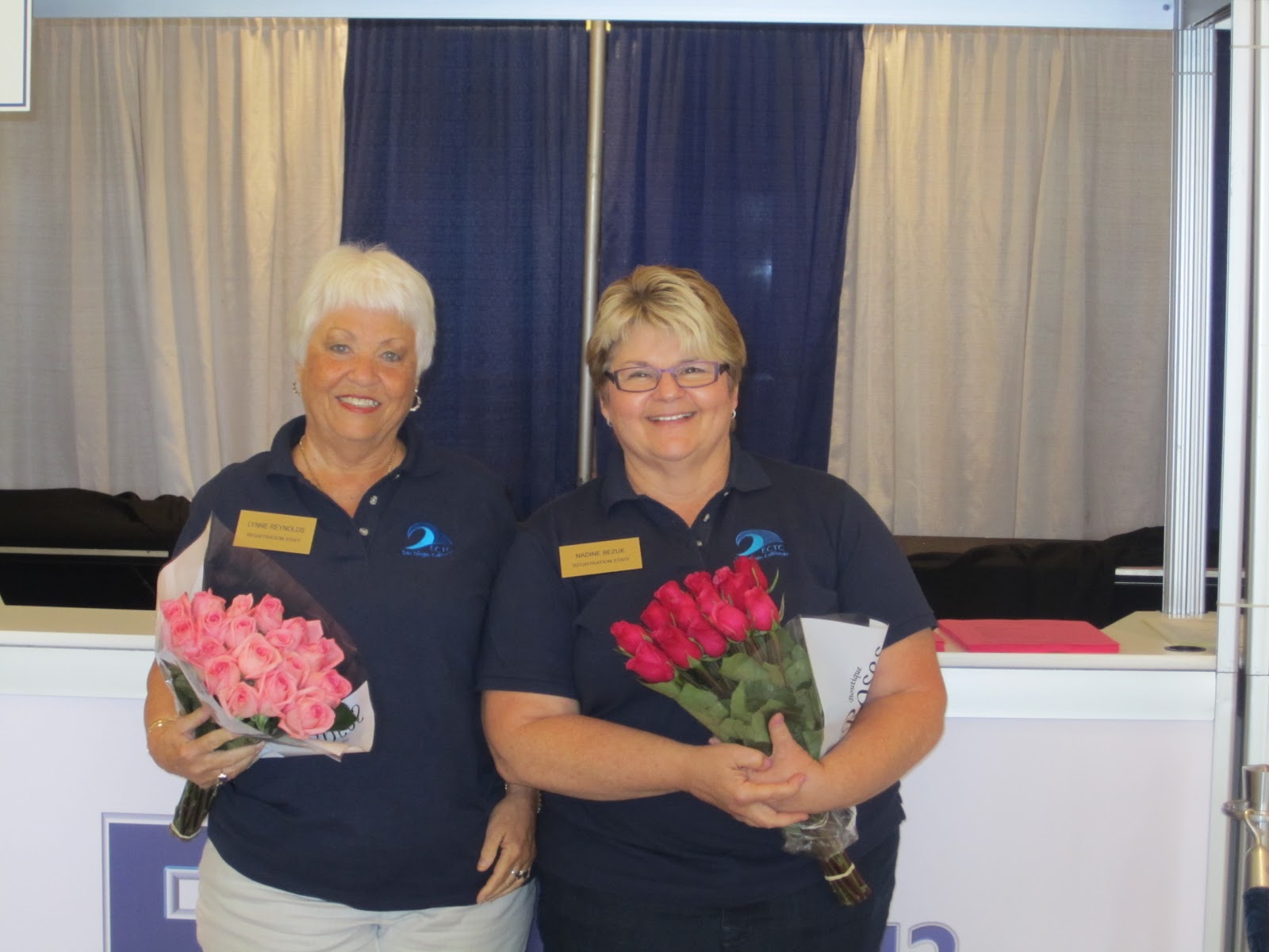
The committee gave special thanks to two wives who have been helping with registration and anything else the conference needed for over a decade — Lynn Reynolds and Nadine Bezuk:
IEEE CPMT AWARDS
An important part of every ECTC is the IEEE CPMT awards ceremony. This year’s CPMT officers include : Ricky Lee (President); Jie Xue (Technical VP); Jean Trewhella (VP Conferences); Kitty Pearsall (VP Education); Wayne Johnson (VP Publications) .
The theme of this year’s meeting was "going on safari" (I assume tied to the San Diego Zoo) so that’s a safari hat on Ricky’s head in case you’re wondering.
This year’s award winners included:
 IEEE CPMT Field Award to Dr. Mauro Walker (Motorola – Retired)

As IFTLE has described previously, the Field award is the highest level award in IEEE for any given division, so this is the highest award available in the world for IC packaging. This year’s recipient Mauro Walker has had a long career of accomplishment in the advancement of electronic manufacturing and manufacturing technology in industry, academia and professional societies. His leadership in Motorola in the 1970s and 1980s drove the component packaging miniaturization that was necessary for portable communications such as cell phones pagers and two way radios. He established advanced manufacturing technology centers within Motorola which developed many innovations for high speed surface mount assembly.

He is the previous recipient of the IEEE’s Special Manufacturing Technology Award and the Society for Manufacturing Engineers’ "Total Excellence in Electronic Manufacturing Award." Walker is an IEEE fellow and founder of the IEEE International Electronic Manufacturing Technology Symposium (IEMT).
Having worked on technology introduction programs with Motorola during this time, I can tell you that this is a well deserved award. There was no one introducing technology like bumping and chip scale packaging into consumer products better or earlier than Motorola in those days.  Congrats Mauro!
IEEE CPMT Dave Feldman Award to Dr. Phil Garrou (Microelectronic Consultants of NC)

The Dave Feldman award is for extended and extraordinary leadership in the IEEE CPMT society. It is named after Dave Feldman who was a key player in Bell labs in the 1950 and 60s and started the ECC (the predecessor  to ECTC) in 1950. I am humbled to say that this year’s winner was yours truly. After the luncheon, a bright eyed 20 something engineer came up to me and asked exactly what you had to do to win an award like this, i.e what made me stand out from the other folks in a position of leadership in this large organization. He probably expected some quick cliche answer, but instead I bent his ear with some philosophy. But seriously, the two actions that I am most proud of during my Presidency have to be (1) installing 1 man one vote on a global basis. While Rao Tummala certainly drove the global expansion of the CPMT society during his 4 years, when I took over as President our board of Governors still had a European and an Asian representative which the rest of the US elected body "selected" to represent the non US members. After developing enough internal consensus,  I pushed to have non US members select only their own representatives and to have each region represented based on the number of members in those regions. Seems logical enough, but somebody had to actually push to get it done and that was me. FYI – it is no coincidence that our last president was from Germany and our current president is from Hong Kong – we are now truly a global society which was Rao and my original dream. PS – growth in both these areas continues – this year both Europe and Asia representation went up by one BOG member while the US went down by two. (2) the complete ownership of the ECTC. Since I started going to the ECTC in the mid 1980s, I was always confused by the co-ownership (IEEE CPMT and EIA) that existed. As I took over as President this did not clarify itself, but rather became more and more confounding. ECTC was, and is the flagship conference of the CPMT, but it was only partially controlled by our IEEE organization. So my second "quest" was to buy out the EIA. I was not able to conclude this during my term, but after convincing incoming President Bill Chen of the logic in this, we moved forward during his presidency to amicably conclude this transaction. That’s it, although it may seem trivial to you the reader, that’s what I think my lasting stamp on the organization will forever be. 

Sustained Technical Contribution Award – Tseung-Yuen Tseng (Chiao-Tung Univ Taiwan)

The sustained technical contribution award went to Tseung-Yuen Tseng of National Chiao-Tung Univ in Taiwan where he is University Chair Professor in the Department of Electronics Engineering and the Institute of Electronics. Dr. Tseng’s professional interests are electronic ceramics, nanoceramics, ceramic sensors, high-k dielectric films, ferroelectric thin films and their based devices, and resistive switching memory devices. He has published over 300 research papers in refereed international journals. He invented the base metal multilayer ceramic capacitors, which have become large scale commercial product. Dr. Tseng was elected a Fellow of the American Ceramic Society in 1998, IEEE Fellow in 2002 and MRS-T Fellow in 2009.

Exceptional Technical Achievement Award – Andrew Tay – National Univ of Singapore
Electronics Manufacturing Technology Award – Chin Lee – Univ of California
Outstanding Young Engineer Award – Mudasir Ahmad – Cisco
IEEE Fellows – Mao Jun Fa (china), Yogendra Joshi (USA), Pradeep Lall (USA), Mike Li (USA), Anthony Oates (Taiwan), William Palmer (USA), Enboa Wu (China)
For all the latest on 3DIC and advanced packaging stay linked to IFTLE………………..

IFTLE 106 2012 Symp on Polymers for Microelectronics

This was the 15th year that polymer suppliers and users have met in Wilmington DE to discuss the latest advances in polymeric materials. All of the big boys were there including : HD MicroSystems , Dow, JSR, Asahi Kasei, Toray, Nippon Kayaku (MicroChem), AZ and Hitachi Chemical.

Certainly the most interesting bit of information that I learned about a materials supplier was that Alpha started its business in 1704 making cannon balls… cannon balls to solder balls — now that’s a roadmap for miniaturization!

Certainly the main theme, as you shall see below, was the development of low curing temperature polymers that could come close to matching epoxies curing temp (i.e ~175C) while maintaining improved thermal and mechanical properties.   

My plenary presentation was based on the new Yole report "PolymericMaterials for 3DIC & WLP Applications"

Basically over the last 50 years the industry has developed five  basic chemistries for the microelectronics industry. In chronological order they would be epoxies, siloxanes, polyimides, BCBs and PBOs.

(Click on any of the images below to enlarge them.)

If we look at the properties that are important to all or most functions / applications we find 4 broad categories including electrical, mechanical, thermal and misc. (other).

The half dozen key functions that we want these polymers to fill and the seven wafer level applications that we are looking to use them in are depicted below.


Yole projects a 26% CAGR for WL applications over the next few years which will expand the current market to near $1B with significant expansion of applications other than FC bumping.
Since new materials take decades and 10s of millions of dollars to develop, those in the business of wafer level packaging over the next 5-6 years will basically have products from these 5 chemistries to serve the functions for the listed applications.  

The theme for permanent dielectric suppliers at this meeting seemed to be positive tone aqueous developable dielectrics with sub 200C curing temperatures and resultant low stress. The newer packaging scheme such as eWLB require this evolution in dielectric materials because the wafer substrate is epoxy based and  cannot survive the processing temperatures needed to cure polyimides or most PBO and BCB materials. Also, ICs with embedded memory are very sensitive to process temperatures and survivability drops dramatically with increase in temperatures. Lastly, advanced technology nodes such as 32 and 22 nm use lower-k dielectric materials, which are sensitive to the high stresses generated by higher curing temperatures.
Toray is offering a LT series low-temperature curing,  positive-tone photosensitive PI coating with a 170- 200C curing temp and resultant 13 MPa thermal stress. With a tensile strength = 100 MPA, elongation of 30% and Modulus of 2.5 GPa . While the residual stress is reported as 13 MPa, the CTE is troubling at 70 ppm. Asahi Kasei is offering  BM series PIs which reportedly can cure as low as 200C with a Tg of 220C, a CTE of "50-60" and a stress of 19 MPa . HD Micro reported on a new PBO, 8850, with reported better chemical resistance, which can be cured at 250C. JSR reported on their WPR series dielectrics which for positive tone are cresol based with rubber reinforcement. While they can be cured at 200C and have low residual stress ( 20 MPa), their tensile strength (80 MPa) and elongation (7%) are low for permanent dielectrics.  Dow chemical reported on their aqueous developable P6505 BCB which cures as low as 180C (3 hrs) with a resultant stress of 25 MPa. Most of the properties look like the BCB 4000 series with a notable exception that water absorption has risen from 0.2% to 2% for the new version. 
Toray also introduced a siloxane product to replace acrylics for optical applications such as CMOS image sensors, LCD and OLED displays and solar modules. It is 99% transparent at 400 nm and is much more thermally stable than the typical acrylics.
As a general comment, all of these materials are beginning to look like one another which may or may not be a good thing for the industry. As IFTLE has said many times before, you must determine what properties are most important for your application and choose your dielectric accordingly. 
Next week we begin our coverage of the ECTC conference. For all the latest in 3DIC and advanced packaging stay linked to IFTLE………………….


IFTLE 105 TSMC Tech Symp; UMC Investment; Latest rumors on IBM, Intel, Samsung and Apple

TSMC Tech Symp

At the 2012 TSMC Tech Symp in April they revealed Reference Flow 12 which shows 2.5/3D firmly entrenched in the TSMC roadmap.

Recent blogs have discussed TSMCs move into the 3D and advanced packaging area. [see IFTLE 94 “Experts discuss InterposerInfrastructure at IMAPS DPCand IFTLE 102 “3.5D interposer technology could somedayreplace PCBs" — TSMC’s Doug Yu” ]

Indeed TSMC isnow showing slides where only the memory and substrates are coming from external sources, making them a turnkey solution for what they are now calling 3.5D [link].

UMC stays in the game
In IFTLE 88 “Apple 2.5D Rumors; Betting the ranchâ??¦” we drew an analogy of putting new fab production in place to a poker game in the Wild West – or betting the ranch. Well, the recent announcement by UMC certainly had them tossing their chips into the center of the table matching the recent capacity announcements by TSMC and Global Foundries. The UMC 300mm Fab 12A Phase 5 & 6 in Tainan will extend 28nm production. P5 & P6 will provide advanced 28nm, 20nm, and 14nm capacity, and is scheduled for equipment move-in during the second half of 2013. Total cleanroom area is 53,000m2 and will be capable of 50K wafers per month, bringing total monthly design capacity for Fab 12A to 130K wafers. With the planned P7 & P8, the eight phase fab complex will have a total design capacity of 180K wafers per month.
Cumulative capex for UMC’s Fab 12A phases 1-4 is projected at $ 8 billion, with P5 & P6 to add nearly $ 8 billion more. There are further plans for P7 & P8. As we said earlier, only the big time players are sitting at this table. With such investments, UMC is certainly showing that they intend to stay in the game.
 They also announced continued activity in “â??¦ BSI CMOS image sensor, 2.5D interposer, and 3D IC TSV to provide a truly comprehensive, leading foundry technology platform”  
Rumors from the ECTC
The IEEE ECTC meeting was last week and for those of you who are unaware, it is the number one show for advanced packaging in the industry. 2.5/3D has grown steadily at this conference and it now appears to be nearing 50 % of the ECTC content [ 50% of 6 parallel sessions for 2.5 days] . There were no major announcements at the meeting, but there were some interesting rumors. My filtering criteria is that I must hear the rumor at least twice from separate sources before I report it on to you.  None of these could be substantiated by the parties involved, but that is not surprising.
 IBM Power8 processor
IFTLE has reported before that rumors were swirling that a future generation of the IBM power chip processor would be using a 2.5D interposer configuration. Very strong, multisourced rumors at ECTC persist that the Power8 is currently undergoing testing in IBM servers and we could be hearing about this major interposer announcement “soon” .
 Intel
If your like me, you have been waiting for 5+ years for the imminent 3D announcement from Intel. Recall that we have been told that the technology is ready but it would be up to the product departments as to when to introduce it. Well, not so good news here. The rumor going around is that we are probably looking at 2017 when 450 is introduced. (Don’t shoot me I’m just reporting the rumor. ) If anyone from Intel would like to deny this and give IFTLE better information please send me an email.
Apple / TSMC / Samsung
Back in IFTLE 88, “Apple 2.5D rumorsâ??¦â??¦” (which I’m told was the most read IFTLE blog of all time) we discussed the fact that TSMC and Samsung are in competition for the next generation , the A6, processor for the Apple iPod, iPad etc.. Although everything is hush, hush, it is clear that TSMC is at least developing prototypes based on their interposer technology. It is unknown whether Samsung is doing the same (but we can hope so).  Two opposing  rumors were making the rounds at ECTC. Rumor 1 had Samsung about to make a 2.5/3D announcement, but rumor 2 had Samsung developing an “unknown technology” that negated the need for TSV and leading them to the conclusion that 2.5/3D would not be needed in the future. The Samsung clamp down on the release on any information on 2.5/3D remains â??¦hermetic . Yes these could in fact be the same rumor, but I, for one, hope not.
Lots more from the ECTC over the next few weeksâ??¦â??¦â??¦â??¦â??¦..
For all the latest on 3DIC and advanced packaging stay linked to IFTLEâ??¦â??¦â??¦â??¦â??¦â??¦â??¦â??¦â??¦â??¦â??¦â??¦â??¦â??¦â??¦.

IFTLE 104 IMAPS DPC Part 2; Over 50% of TI WB Converted to Copper

Continuing with key presentations from the 2012 IMAPS Device Packaging Conference in Ft McDowell AZ.

Tezzaron Process Technology
Bob Patti showed off two Centip3De, a 3-D IC stack using 128 ARM Cortex M3 cores and 256 Mbytes of stacked DRAM from the Univ of Michigan and the 3-D MAPS, a massively parallel processor using 64 custom cores stacked with a block 256 kilobytes of scratch pad memory from Ga Tech. For more details on these see IFTLE 93, "2.5/3D at the 2012 ISSCC".

(Click on any of the images below to enlarge them.)

Amkor Discusses 2.5/3DIC

Amkor’s Ron Huemoeller reported that 3D vertical stacking is:

memory and application processor driven
– today focused on 28 nm CMOS and moving to 22 nm
– application processors are near exclusively moving to OSAT finished wafer process flows
Whereas 2.5D Interposers are:

–  network, CPU and GPU driven
…….. mother boards reduced from 10 to 6 layers
…….. reduce chip mask layers
…….. smaller x, y dimensions
– focused on large package bodies (40 -90 mm , near retical sized Si)
  both foundry and OSAT wafer flow processes being used
 

He sees both dis-integration of large logic blocks and separation of functions

– allows focus of specific functions which require  leading process nodes
– improves wafer yield
– reduces time to market
– reduces mask layer count at advanced process nodes

Concerning the interposer supply chain:

– laminate (which can theoretically be delivered in large panel format (i.e. 500 x 500 mm ) are being investigated by several "elite substrate manufacturers" [ Unimicron, DNP, Shinko, Kyocera]. Limited to 8 um L/s and 40 um vias on 85 um pads today. 5 um l/s will require stepper and better resists which change the economics. 5 um L/S thought to be many years away. Latency issues will limit adoption as will limitations in va/pad design rules.

– glass can be delivered in large panel or wafer format. Several glass companies [Hoya, Corning, AGC] are investing in capability to support glass interposer technology. Glass faces challenges for CMP / damascene processing.

– silicon in 200 or 300 mm several companies supporting silicon interposers in idle foundry space on legacy node technologies. Amkor finds only 3 foundry players committed to delivering "fine featured" interposers [ TSMC, GF, UMC] with TSMC the only one currently delivering in any quantity.

According to Amkor several foundry sources are interested in manufacturing Si interposers and a couple are already delivering fully functional wafers. Currently design rules  "are aggressive" i.e. less than 2 um L/S and 5 um vias.

Amkor indicated that the predominant interposer designs are what IFTLE has been calling "fine featured" as follows:

When looking at TSV products expected to enter the market in the next few years, Huemoeller offered the following roadmap.

TI Promotes Cu WB

TI has recently announced that all 7 TI internal assembly and test sites are now converted to Cu WB. 6.5B devices have been shipped in Cu WB with conversions continuing. TI which started their Cu WB studies in 2003 are in HVM at the 65 node and have qualified down to the 45 node. 50% of all their interconnect wire is now Cu.
Analog, wireless and embedded products in BGA and leadframe packages are all qualified. Cu shows less wire sweep during package molding and since it has better inherent thermal conductivity it shows better battery life. Next TI will be looking at "high rel" applications such as automotive, military and down hole drilling with Cu wirebonding.

For all the latest in 3DIC and advanced packaging stay linked to IFTLE……………….

IFTLE 103 2012 IMAPS AZ Device Pkging Conf; Fujitsu Low Temp Cu-Cu Bonding

It’s been over for a few months now, but IMAPS was a bit slow this year gathering the presentations from their device packaging conference, This is however understandable and excusable due to the untimely death of IMAPS employee Jackie Joyner. So let’s begin looking at the 2.5/3D and significant advanced packaging papers.

SSEC Wet Etch for Via Reveal

Laura Mauer of SSEC discussed silicon wafer thinning to reveal Cu TSV. The standard via reveal processis shown below. SSEC contends that a KOH wet etch process can be used for the final Si removal without etching the oxide liner. This can be sealed with oxide/nitride and then CMP’ed to expose the Cu vias.

Wet etch with HF/HNO3 has also been proposed by ASET and shown to have minimal impact on the electrical characteristics of the transistors [link].
Asahi Glass TGV (Through Glass Vias)
Takahashi of AGC discussed the fabrication of TSV in glass. They have been able to fabricate TGV with a  193 nm ArF excimer laser by using short pulse width (20-30 ns). The TGV do have significant slope. Better results are achieved when the glass is processed at elevated temperature ( i.e 200C)

Focused electrical discharge can also be used to process TGV in less than 1 ms. AGC claims that there is no physical limit to TGV diameter using electrical discharge. Electrical discharge TGV show smooth sidewalls and rounded via edges. Similar to the laser process the process requires no masks.
Underfill options – Hitachi, Lord, Dow
Hitachi Chemical discussed non cnductive pastes and films. Packaging in general is moving towards finer pitch and smaller gaps requiring a change in underfill materials and procedures.  NCP and NCF applicable for fine pitch and narrow gaps. In terms of pad finish, Hitachi notes that Cu with OSP "is more difficult to have a good connection."
Lord detailed their screen printable NCP ( Tg = 166 C; Mod = 4.1 Gpa) with built in fluxing agent which allows them to do cu-cu bonding on oxidized cu studs. Similarly Dow presented data on their new pre applied underfill (WUF) films with the following materials properties:

Vacuum lamination is preferred and curing is done at 175C for 1 hr. Voiding seen after bonding can be eliminated by pressure curing or optimizing the film thickness. Initial reliability tests indicate good adhesion through MSL-3- 260 C and TCT cond B.
Fujitsu Low Temp Copper-copper Bonding
Fujitsu described further advances in their low temp Cu-Cu bonding technology [link].
Their unique process uses a diamond bit milling machine to achieve a highly uniform and highly polished (7 nm surface vs 210 as plated) which can be thermo-compression bonded at RT and shows grain growth across the interface at 200 – 250C vs 350 C+ for a  standard CMP’ed surface.


Underfill and Cu bumps can be simultaneously cut together by diamond bit with no residue on bump, but hybrid copper/underfill interface exposed to formic acid before bonding "could not sustain arranged location during bonding process." However, if the interface is bonded first and then exposed to formic acid, "partially exposed," clearly grain growth occurs as low as 140 C.


For all the latest on 2.5/3D IC and advanced packaging stay linked to IFTLE…………………….

IFTLE 102 â????????3.5D Interposers to someday replace PWBsâ???????? – TSMC; GF engaging with 3D customers; Intel predicts Consolidation

3.5D Interposers

At the 15th Symposium on Polymers for Microelectronics held last week in Wilmington DE, TSMCâÂ??Â??s Doug Yu, Sr. Dir. of front end and back end technology development,  challenged the current nomenclature for interposers and suggested that the more versatile interposer technology should be called 3.5D instead of 2.5D since it is, and will be, capable of much more than the simple 3D stack.

The term 2.5D is usually credited to ASE’s Ho Ming Tong who ~ 2009 (or even earlier)  declared  that we might need an intermediate step towards 3D since the infrastructure and standards were not ready yet.  The silicon interposer, Tong felt, would get us a major part of the way there, and could be ready sooner than 3D technology,  thus the term 2.5D, which immediately caught on with other practitioners.

Yu’s new position is that interposer technology actually is more versatile and thus should be called 3.5D since it  not only offer a better thermal solution than 3D, but "…can  some day replace most of the high density PC boards." Yu’s position is that this modular silicon technology will need minimum low density PCB substrate to connect the functions that have been fabricated on silicon and will be, in essence, the perfect "fab centric" solution. Yu proceeded to show how future smartphones and tablets could be made up of such simple 3.5D silicon modules. More from the Polymers for Electronics meeting coming soon at IFTLE.

Global Foundries 2.5/3D Announcement

GLOBALFOUNDRIES has announced the installation of TSV production tools for the company’s 20nm technology platform. CTO Bartlett announced that they were  "…engaging early with partners to jointly develop packaging solutions that will enable the next wave of innovation in the industry." The first full flow silicon with TSVs is expected to start running at Fab 8 (Saratoga NY)  in Q3 2012 with mass production expected in 2014. GF is also preparing for  a 2.5D line within its Fab 7 facility in Singapore with a similar time schedule as the 3D line in the United States.

While arch competitor TSMC has announced a one-stop-shop turnkey line which includes all of the assembly and test steps traditionally handled by the OSATS [see: "TSMCrepeats call for foundry-centric 2.5/3D industry"], GF proposes to handle  TSV fabrication (Cu , vias middle) and other front-end steps while typical backend  processes such as temporary bonding/debonding, thinning, assembly and test will be done by their OSAT partners such as Amkor [ see IFTLE 65 "….. GLOBALFOUNDRIES Packaging Alliance…" GlobalFoundries reports that they will define a PDK with its partners, initially they are looking at 6 um vias on a  40-to-50um pitch.

Intel agrees – Its all in the Economics

At the recent Intel analyst day CEO Paul Otellini CEO predicted that the increasing cost of manufacturing in the IC industry would result in consolidation that  will "…only leave two or three companies at the leading edge of chip design." Otellini reports that "Gordon Moore predicted a thinning out of chip fabrication facilities once the cost of a new 200mm wafer manufacturing plant hit $1bn, but he was a little too early."

With the cost of a 300mm fab expected to exceed $5B at the 28 nm node and  450mm wafer fabs that are projected to cost more than $10B apiece few companies will have enough volume to absorb such costs.  

Readers of IFTLE know that we have been predicting this outcome for several years [ see PFTLE "IC Consolidation, Node scaling and 3DIC". Nice to see that Intel  agrees, although this will severely limit options for customes of the latest node technologies. 

If you look at this strictly in terms of economics, HVM players at 22 nm should be limited to :

Logic – Intel, Samsung, ST Micro

Memory – Samsung, Toshiba, Micron/Elpida, Hynix ?

Foundries – TSMC, GF

That’s less than 10 total players on the leading edge moving forward. Better start getting used to it !

For all the latest on 3DIC and advanced packaging stay linked to IFTLE……………….

IFTLE 102 “3.5D Interposers to someday replace PWBs” – TSMC; GF engaging with 3D customers; Intel predicts Consolidation

3.5D Interposers

At the 15th Symposium on Polymers for Microelectronics held last week in Wilmington DE, TSMC’s Doug Yu, Sr. Dir. of front end and back end technology development,  challenged the current nomenclature for interposers and suggested that the more versatile interposer technology should be called 3.5D instead of 2.5D since it is, and will be, capable of much more than the simple 3D stack.

The term 2.5D is usually credited to ASE’s Ho Ming Tong who ~ 2009 (or even earlier)  declared  that we might need an intermediate step towards 3D since the infrastructure and standards were not ready yet.  The silicon interposer, Tong felt, would get us a major part of the way there, and could be ready sooner than 3D technology,  thus the term 2.5D, which immediately caught on with other practitioners.

Yu’s new position is that interposer technology actually is more versatile and thus should be called 3.5D since it  not only offer a better thermal solution than 3D, but "…can  some day replace most of the high density PC boards." Yu’s position is that this modular silicon technology will need minimum low density PCB substrate to connect the functions that have been fabricated on silicon and will be, in essence, the perfect "fab centric" solution. Yu proceeded to show how future smartphones and tablets could be made up of such simple 3.5D silicon modules. More from the Polymers for Electronics meeting coming soon at IFTLE.

Global Foundries 2.5/3D Announcement

GLOBALFOUNDRIES has announced the installation of TSV production tools for the company’s 20nm technology platform. CTO Bartlett announced that they were  "…engaging early with partners to jointly develop packaging solutions that will enable the next wave of innovation in the industry." The first full flow silicon with TSVs is expected to start running at Fab 8 (Saratoga NY)  in Q3 2012 with mass production expected in 2014. GF is also preparing for  a 2.5D line within its Fab 7 facility in Singapore with a similar time schedule as the 3D line in the United States.

While arch competitor TSMC has announced a one-stop-shop turnkey line which includes all of the assembly and test steps traditionally handled by the OSATS [see: "TSMCrepeats call for foundry-centric 2.5/3D industry"], GF proposes to handle  TSV fabrication (Cu , vias middle) and other front-end steps while typical backend  processes such as temporary bonding/debonding, thinning, assembly and test will be done by their OSAT partners such as Amkor [ see IFTLE 65 "….. GLOBALFOUNDRIES Packaging Alliance…" GlobalFoundries reports that they will define a PDK with its partners, initially they are looking at 6 um vias on a  40-to-50um pitch.

Intel agrees – Its all in the Economics

At the recent Intel analyst day CEO Paul Otellini CEO predicted that the increasing cost of manufacturing in the IC industry would result in consolidation that  will "…only leave two or three companies at the leading edge of chip design." Otellini reports that "Gordon Moore predicted a thinning out of chip fabrication facilities once the cost of a new 200mm wafer manufacturing plant hit $1bn, but he was a little too early."

With the cost of a 300mm fab expected to exceed $5B at the 28 nm node and  450mm wafer fabs that are projected to cost more than $10B apiece few companies will have enough volume to absorb such costs.  

Readers of IFTLE know that we have been predicting this outcome for several years [ see PFTLE "IC Consolidation, Node scaling and 3DIC". Nice to see that Intel  agrees, although this will severely limit options for customes of the latest node technologies. 

If you look at this strictly in terms of economics, HVM players at 22 nm should be limited to :

Logic – Intel, Samsung, ST Micro

Memory – Samsung, Toshiba, Micron/Elpida, Hynix ?

Foundries – TSMC, GF

That’s less than 10 total players on the leading edge moving forward. Better start getting used to it !

For all the latest on 3DIC and advanced packaging stay linked to IFTLE……………….

IFTLE 101 Advanced Packaging at IMAPS MINIPAD part 2

Continuing with our examination of advanced packaging at the 2012 IMAPS MINIPAD.

ST Micro reported on stress induced fine pitch copper pillar failures. Compared to solder bump, Cu pillar bumping is known to possess good electrical properties, better electromigration performance and better thermal fatigue resistance . The only drawback is that Cu pillar bump can introduce high stress due to Cu higher stiffness compared to the solder material. Therefore, the stress induced failures become a major issue when Cu pillar bump is built on low k or extreme low k (ELK) chips. In this ST Micro study, fine pitch copper pillar has been assessed vs polyimide effectiveness for fine pitch Cu pillar interconnections having small pillar diameter.

(Click on any of the images below to enlarge them.) 

Vehicle1 (package 2 configuration) used extreme lowk ILD materials. Die were attached on the substrate without underfill and underwent several die attach reflow cycles to induce failure and define the more robust configuration. The no PI leg did not evidence any defect up to 20 reflows but the PI passivated leg showed 100% failure after 20 reflows which appear to be stress induced failures ( likely to be crack in aluminum pads ).


Results after reliability tests show that the implementation of polyimide for fine pitch Cu pillar is not obvious. Thus, in the case of PI configuration, failure analysis reveals three main failure modes: delamination at the Bump/PI/pad and copper stress voiding in the pad metal in stacked vias structures, both occurring during thermal cycles. Delamination in the low-k layers has been also found for the highest die size in the PI configuration. All those analyses have revealed that for the tested configurations, higher stress has been observed with the PI configuration compared to the no PI one.

FEA was done to better understand these results. In the No Polyimide configuration, the stress is spread along the pad structure thanks to the higher copper contact. Indeed, the passivation layers (i.e. SiN and PSG layers) have sufficient mechanical properties to transfer the stress to the beneath layers. In the PI configuration, high peak stress is observed beneath the Copper/Aluminum interface. On the contrary, in the No PI configuration, the stress is spread along the pad structure thanks to the higher contact of Copper pillar bump.

STATSChipPAC looked at some "Advanced Ultrathin eWLB-PoP solutions." eWLB has been introduced into production to allow for higher ball count WLP, by extending the package size beyond the area of the chip. There is also great opportunity related to a 3D variation of eWLB which would allow for mounting of components or another package on the top surface with thinner profile and PoP (Package-on-Package) technology.
The table below shows reliability for such stacked test vehicles.
Bernd Appelt of ASE continued the theme of thinner is better with his presentation "Ultra Slim Packages with Ultra Slim Substrates" There is no question as the figure below shows devices continue to get thinner.

 JEDEC package heights are defined as follows:

The ASE package family fits these dimensions as follows:
Substrate thickness vs package thickness are shown on the following chart:
The ASE embedded technology a-EASI (adv embedded assembly solution integration). They are undergoing customer evaluation with embedded actives and passives.
FCI presented the latest n their ChipletT(TM) and ChipsetT(TM) embedded die fan-out packaging based on multilayer flex. We discussed this technology in detail last fall [see IFTLE 83, "Orange County 3DIC Workshop"]
Below we see a nice example of what can be done with this technology, i.e a 50% reduction in footprint by embedding the ASIC die.


For all the latest in 3DIC and advance packaging stay linked to IFTLE………………….