Insights From Leading Edge

Yearly Archives: 2012

InterNepcon, Loss of a Dear Friend

At the recent InterNepcon Japan Exposition held at the Tokyo "big site" their "IC Packaging Technology Expo" contained some new information and some retreads that we have seen on IFTLE previously. Below I’ll cover a few new items that may be of interest to you.

TI’s Mark Gerber, a key player in bringing up their Cu pillar technology at Amkor addressed 3D packaging technology for next generation devices. Mark broke out current FC interconnect technologies into the following 4 categories indicating that fine pitch gold stud bumping was confined mainly to Japan.

(Click on any of the images below to enlarge them)

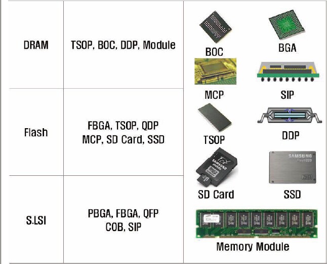
Sung-Il Cho of Samsung’s test and package center looked at Samsung’s Packaging Roadmap. He offered the following categorization for their DRAM, Flash and system LSI chips…

…and the following roadmap for flash technology development for solid state drives. Consistent with their corporate policy of holding new technology information "close to the vest" their inputs on 3D packaging with TSV were either ITRS roadmap slides or Yole roadmaps that have been published on these IFTLE pages before.

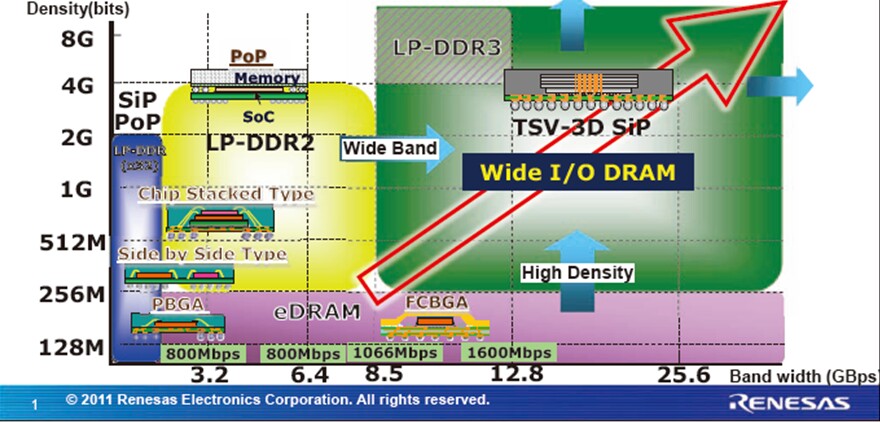
Keiichirou Kata of Renesas Advanced Package Development Dept. addresses their packaging roadmaps. He sees the major developing areas as FC BGAs, WLP and what he calls 3D Jisso (3D IC integration). Their FC technology roadmap is driven by desire for tighter pitches.

28 nm node chips will see a move to 108 um pitch and copper pillar bumps by the end of 2012.

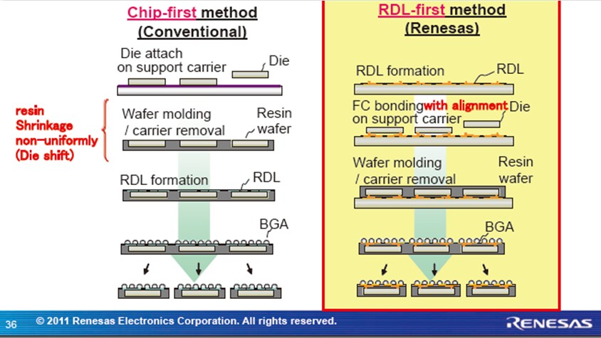
Their proposed fan out WLP is an RDL first technology which they contend eliminates the issues of chip movement due to mold compound shrinkage.

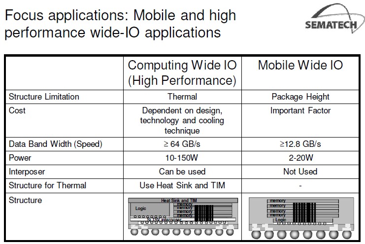
They are moving to wide IO DRAM standards for low power DDR3 and beyond.

Ryoji Matsushima from Toshiba’s Memory Packaging Engineering Dept. discussed equipment materials and processing issues for thin memory packages. High memory capacity, high memory access speed and thinner packages all point towards memory stacking with TSV.

Technical issues with thin packages are shown on the slide below.

In Memorium: Jackki Morris Joyner

This past week I was attending the IMAPS Device Packaging Conference in Ft McDowell AZ (coverage coming in a few weeks). Those of you who are long time readers of IFTLE know I am there every year and strongly support this IMAPS conference. In the end, what separates societies is people not content. Part of what makes IMAPS great to work with has been Jackki Morris, or as we knew her post marriage Jackie Morris Joyner. When she first told us of the impending marriage and that she was becoming Jackki Joyner we all teased her asking her to run around the buildng for us ( for our non US friends this is the name of a famous US Olympic runner) and she laughed along with us. Jackki was the kind of person who made your life better for having talked to her on the phone or corresponded by email. Everyone asks "how’s it going" but she meant it. She genuinely cared about people… you just could tell.

The last time I talked with Jackki she was working the IMAPS table with her husband Cliff Monday night. When she saw me she gave me a hug and she turned on her computer and showed me pictures I had sent her of my grandaughters a few years ago. She had pages and pages of pictures of all the friends she had made through IMAPS because she just was that way. We shared funny stories of past conferences and laughed before I let her get back to work.

The next morning she was noticeably missing and Exec Dir Michael O’Donoghue revealed to several of us that Jackki had become quite ill during the night. By the time she made the hospital her heart had stopped several times and she was in intensive care with Cliff by her side. This cast a pall over the rest of the meeting and she remained in intensive are as we all left the meeting to go home. By the time I arrived home Friday she had passed away. The world is truly worse off today because this caring, loving person is gone.

Our prayers are with Cliff and her family

Anybody here seen my old friend Jackki
Can you tell me where she’s gone
She cared and shared with a lot of people
But it seems the good they die young
I just turned around and she’s gone

IFTLE 91 IEEE 3DIC Japan 2012 part 2

Continuing to examine presentations from the 3rd Int IEEE 3DIC Conf held in Japan in Feb 2012.

Copper Protrusion

In the last several years PFTLE and IFTLE have brought copper protrusion to the forefront as an issue [see "Researchers Strive for Copper TSV Reliability" Semi Int, 12/03/2009] and reported on technical solutions as they appeared from IMEC [see IFTLE 6 "Cu-Cu and IMC Bonding Studies at 2010 ECTC…"]; TSMC [see IFTLE 34, "3DIC at the 2010 IEDM"] and others. IME has now reported on their study of 5 um x 50 um Cu TSV as they were annealed from 250 to 450C.

Cu expands vertically because it is constrained by the surrounding silicon substrate. Because it expands plastically it does not return to its original length when the sample is cooled down.

(Click on any of the images below to view the full-size version)

The effects of anneal temp, anneal time, via diameter and via depth are shown below where "room temp" refers to the protrusion present after anneal and return to room temperature and high temp refers to protrusion after anneal while still at the elevated temperature. As with previous studies they found that CMP after anneal retards any further protrusion if the temperature is again elevated.

Bottom line is that protrusion is minimized by small diameter, low aspect ratio TSV.

Samsung System LSI Division has also looked at the Cu protrusion issue and report similar results i.e that Cu protrusion can be reduced by heat treatment before CMP and that Cu protrusion and delamination strongly depend on TSV dimensions.

When the via diameter was in zone A all the vias showed high Cu extrusion and via delamination, but TSV diameters from zone B showed no problems.


Micro-cracking caused by Lateral Extrusion

Conference Chair Koyanagi and co-workers at Tohoku Univ also examined TSV dimensions and the effect of high temp annealing. An array of Cu TSV with diameters ranging from 3 to 30 um at three different pitches were annealed from 200 to 400C. Both the lateral and vertical protrusion of the copper was monitored.

Again larger diameter TSV (at a constant depth) show higher extrusion, but also that lateral extrusion (extrusion in the x-y after Cu has protruded from the surface) increased with anneal temp. For example 5 um TSV on a 10 um pitch extrude laterally 2 um at 400C. This would put them within 1 um of touching! Stresses induced by the TSV also result in microcracking "…on the periphery of the TSV array and in between the TSV." Careful choice of TSV size and pitch is recommended.

Cu-Cu Direct Bonding

Copper-copper direct bonding continues to be a popular topic due to the promise of fine pitch, low resistance interconnect which are more mechanically reliable than IMC bonding (Cu-Sn-Cu) and should show less electromigration issues. Such processes are currently limited by the required bonding time / temperature which are usually reported as 30 min / 350-400C. The holy grail appears to be a thin die Cu-Cu thermo compression bonding process which requires low bonding temp and pressure.

IMEC and TSMC have studied the direct Cu-Cu bonding of 5 x 40 um TSV with (3) different configurations ; (1) no nail head exposed (Cu CMP’d flat with the oxide surface; (2) flat nail head (cu CMP’d flat and then oxide recessed and (3) natural nail head (stop grind short of the nail head, pull back oxide revealing "dome" shaped copper protrusion. The matching landing pad is a Cu surface CMP’d flat with the oxide surface. After bonding they observed that the "no nail head exposed" and the "flat nail head" sample s delaminated even when the bonding temp and or the pressure was increased. They assumed failure was due to the low % area that is actually used to bond (less than 1%). So, what is good for the design (less than 1% of the area occupied by TSV) is not good for the strength of bonding. The dome bonding was better due to its ability to deform. IFTLE interprets this as an ability of the domed structured to deform allowing shorter TSV to now touch their pads and bond. IFTLE also thinks this is a good reason to look at hybrid bonding schemes such as proposed by Ziptronix [see PFTLE 48, "Opening the Kimono, Ziptronix gives details on DBI Process"] and CEA Leti [see PFTLE 103, "Show me the Copper"]

Stacking of Ultrathin Die

Standard 3DIC thickness has focused around 50 um for the last few years. IMEC has now shared their results of ultrathin (25 um) die stacking.

After temporary bonding and grinding, oxide is pulled back for Cu TSV reveal. The revealed "nail heads" are passivated with 3 um BCB and reconfigured with Cu/BCB RDL. Cu/Sn bumps are then fabricated on the landing pads. The 25um thick die are diced while still bonded to the carrier. They note that "this is required to have enough mechanical support during stacking"

Both NUF and WUF were looked at for underfill solutions. NUF is unfilled polymer dispensed onto the landing die prior to bonding and WUF is filled underfill film laminated to the thinned wafer while still on the carrier.

Issues with NUF were: (1) underfill trapped between the bumps;(2) voids between top and bottom die and (3) induced topography due to underfill shrinkage on cure. Shrinkage of the underfill upon curing and the CTE difference between a microbump and the underfill cause a bending of the die over the ubump connection. For an unfilled underfill and a 25um thick die a 40% increase in the drain current was observed to occur.

After several failed tries, they decided to focus on WUF with 60% filler loading. WUF was vacuum laminated onto the die and gave much better topography and the use of a filled underfill resulted in reduced stress.

They also found that increase in the die thickness from 25 to 50 um resulted in a stress reduction of 3X. Final conclusions were that 50 um thickness die were currently much better option for scalable manufacturable process and that reduction in the TSV diameter from 5 to 3 um will reduce the required KOZ by 64%.

Wireless Product with Design Partitioning

ST Micro and CEA Leti described their program to partition the digital and analog functions of a HD video transmitter onto separate die and stack them using Cu TSV and ubumps.

TSV are 10 um with a 40 um pitch and wafers are 80 um thick. Cu pillar interconnect are 25 um dia and 30 um high. Reliability tests were done at package level using JEDEC level 3. No delamination and no electrical failures were obtained after 1000 cycles.

————–The next IEEE 3DIC Conference will be held in the fall of 2013 in San Francisco————–

Coming up in IFTLE :
-advanced packaging from InterNepcon Japan
-3D as the ISSCC
-detailed coverage on the IMAPS Device Packaging Conference and more

For all the latest in 3D IC and advanced packaging stay linked to IFTLE……………………….

IFTLE 90 Highlights from the IEEE 3DIC 2012 Japan

The 2011 IEEE 3DIC Conference scheduled for Japan, as most of you know, was postponed due to the earthquake and Tsunami issues Japan experienced last year. The good news is that the conference which was postponed till Feb 2012 was held a few weeks ago and was a huge success. More than 250 attendees shared 32 presentations and more than 65 posters concerning the latest breakthroughs in 3D stacking technology.

In the next two blogs we will review what IFTLE considers some of the more important presentations and posters.

Effect of Sidewall Roughness on Leakage Current

Fujitsu has looked at the effect of sidewall roughness on leakage current comparing Bosch etched TSV to ULVAC NLD etched TSV (discussed below). Bosch etched scallops were 72 nm deep and 280 nm long while the NLD etched TSV were ultra smooth. 500 nm of SiON insulator was deposited by low temp PECVD (150C) followed by PVD of 50 nm of TiN and 50 nm of TI to serve as Cu barriers followed by 200 nm of Cu seed.

Leakage current between TSV was measured after annealing for 5 min at from 200 to 400C. Leakage current of NLD is lower than the bosch etched TSV initially and is less than 100x smaller than Bosch after anneal at 400C. These results are correlated with cracking of the insulation layer and subsequent migration of copper. It appears as though sidewall roughness initiates crack growth. Since anneal at 400+ is recommended to reduce the effects of copper protrusion [see IFTLE 6 "Cu-Cu and IMC Bonding Studies at 2010 ECTC…"], it is recommended by IFTLE that such leakage current experiments be run when optimizing Cu anneal process during TSV fabrication to insure integrity of the barrier and insulation layers after processing.

(Click on any of the images below to enlarge them.)
Effect of Sidewall Roughness on Copper migration

Koyanagi and his co-workers examined the influence of copper contamination on device reliability and found that when Bosch scalloping is high, conformal deposition of the dielectric layer and barrier layer is difficult and increases the likelihood of Cu atom diffusion through the thinned barrier on the point of the scallop especially during the thermal temperatures reached during post process thermal anneal.

They fabricated Si trenches with 5 um diameter and 10 um depth with sidewall scalloping of 30 and 200 nm. 100 nm thick oxide and Ta barriers of 10 or 100 nm where deposited by sputtering. This was followed by a 200 nm thick copper seed.

Electrical results showed the 10 nm Ta barrier failed to resist Cu migraion for both the shallow and severe scallops.

ULVAC non Bosch scallop free TSV

The magnetic loop discharge plasma (NLD plasma) used by ULVAC can be used for silicon or oxide etching. The etch profile is controlled by the SF6/O2 ratio. Sidewall roughness of less than 15 nm is obtained.

IMEC and Suss Demonstrate Integration of ZoneBond Process

IMEC has demonstrated integration of the ZoneBond process on their Suss XBC300-LF temporary bond cluster and DB12T peel debonder. The Zone bond process has been described before [see IFTLE 61, "Suss 3D Workshop at Semicon West"]

The bonding material is coated on the wafers in 19.2 +/- 0.4 um thickness. Scanning acoustic microscopy shows that the bonding to a silicon carrier is void free.

After thinning and backside processing the bonded wafers are soaked for a few hours in the adhesive solvent and laminated onto a UV sensitive dicing tape. The carrier wafer is then "peeled" off the device wafer.

The remaining glue is then removed while the device wafer is held on the film frame. Devices are diced subsequent to cleaning.

For all the latest in 3DIC and advanced packaging stay linked to IFTLE………………………

IFTLE 89 Advances in CMOS Image Sensing

It was 5 years ago in the the fall of 2007 when Toshiba first announced the commercialization of TSV in a CMOS image sensor (CIS) [see "PFTLE 12 Imaging Chips with TSV announced…"; PFTLE 16, "More TSV Commercial capacity on line"; PFTLE 24, "ST Micro announces more CMOS Image Sensor Packaging Capacity with TSV"; PFTLE 57 "Toshiba CIS Camera Module Details…"; etc]. The next step of circuit repartitioning and stacking was interrupted by "back side imaging" [BSI], which flipped the chip over and let the light enter through the least obstructed side to let more light in per pixel, which is really important as the pixels are getting smaller and smaller. [see PFTLE 40, "Backside Illumination next for Next Generation CMOS Image Sensors"; PFTLE 46, "on Mechanical Bulls, Rollercoasters and CIS with TSV."

For those of you needing a refresher about how this is done, below is a process flow that Yole Developpment released in 2010 starting with SOI wafers.

(Click on any of the images to enlarge them)

From SOI to Bulk Silicon

Last spring Chipworks announced that Sony had moved from an SOI based process to a bulk silicon process. [link] It is unclear yet whether this will become an industry wide trend.

Chipworks found that while previous Sony BSI sensors they had analysed were fabricated using an SOI starting wafer, with the 1.1µm BSI generation, Sony migrated to using bulk silicon substrates instead of SOI. Chipworks commented that SOI is a more costly substrate, but likely an easier process to implement. They presume that Sony was able to identify the yield limiting contributions from the bulk polishing process, and fine tune the yield to achieve a high yielding and very cost effective process. This process would require a SiO2 bonding process.

In late August Ziptronix announced that Sony had taken a license on Ziptronix’s patents regarding oxide bonding technology for backside illumination imaging sensors [see IFTLE 65, "…Ziptronix Licensing News"]

With BSI fully implemented, it appears that practitioners have now turned their sites back to repartitioning the circuitry and creating true stacked 3D IS structures.

Sony reveals stacking in BSI CMOS Image Sensor

In January Sony announced that it had developed "the next generation back-illuminated CMOS image sensors" by separating the pixel section containing the back-illuminated structure pixels from chips containing the circuit section for signal processing, which is in place of supporting substrates for conventional back-illuminated CMOS image sensors. [link] This results in:
-More compact image sensor chip size
-Higher image quality of the pixel section by optimizing the manufacturing processes for superior image quality on the pixel layer
-Faster speeds and lower power consumption by adopting the leading edge processes for the circuit section

By this stacked structure, large-scale circuits can now be mounted keeping small chip size. Furthermore, as the pixel section and circuit section are formed as independent chips, a manufacturing process can be adopted, enabling the pixel section to be specialized for higher image quality while the circuit section can be specialized for higher functionality, thus simultaneously achieving higher image quality, superior functionality and a more compact size. In addition, faster signal processing and lower power consumption can also be achieved through the use of leading process for the chip containing the circuits. Basically some of the attributes that we have been ranting about for 3DIC for the past 5 years. Samples will be shipped starting in March, 2012.

Poly SI TSV found in the Toshiba BSI CIS from Fujifilm Camera

Chipworks reverse engineering analysis of the Toshiba HEW4 BSI TCM5103PL 16 Mp, 1.4um Pixel Pitch CIS found inside Fujufilm F550 EXR camera. The CIS was fabricated using the Toshiba Oita 300 mm wafer line, using a 65 nm logic process adapted to BSI image sensor production. Fellow SST blogger Dick James [link] was kind enough to share more of the details for our IFTLE readers.

With BSI, the I/O pads end up on the bottom side of the sensor silicon (which is bonded to a handle wafer so the pads are burried). To get to the pads, you need some means of creating a via through the silicon to the front side metal. Very high density arrays of polysilicon filled through silicon vias (TSVs), to form the electrical interconnect between the back side aluminum bond pads and the front side copper lines on the CMOS integrated circuits. These are the first true submicron TSVs that Chipworks has seen deployed in volume production.

Chipworks notes that: "…closely packed, poly-filled submicron TSV… technology is non-trivial to implement. Once mastered and with appropriate economies of scale in play, however, this advanced TSV process saves valuable silicon area and can reduce the size of the camera module."

Applied Materials Targets BSI Sensors Manufacturing

Applied Materials recently announced the Applied Producer Optiva CVD system aimed at the manufacture of BSI sensors. "Emerging BSI image sensor designs present a new opportunity for Applied Materials to provide customers with the technology they need to be successful in this rapidly growing market"

The Optiva low temperature process runs on their Producer platform, capable of depositing low temperature, conformal films that boost the low-light performance of the sensor while improving its durability. The system enhances the performance of the microlens by covering it with a tough, thin, transparent film layer that reduces reflections and scratches, and protects it from the environment. Importantly, the Optiva tool is the first CVD system to enable 95% conformal deposition at temperatures less than 200C. As typical bonding adhesives have thermal budgets of approximately 200C, all subsequent processing on these temporarily bonded wafers must be done below 200C.

iSuppli estimates that 75% of all smartphones will be fitted with BSI sensors in 2014, up from just 14% in 2010. 2014 demand is estimated at 300 million units.

Coming up in IFTLE:
– Advanced packaging highlights from NEPCON Japan
– 3D highlights from the IEEE 3DIC Conference in Japan

For all the latest in 3D IC integration and advanced packaging stay linked to IFTLE……..

Hope to see you all at the IMAPS Device Packaging Conference in Arizona next month!
IFTLE will be hosting a session on 2.5/3D Infrastructure development.

IFTLE 88 Apple TSV Interposer rumors; Betting the Ranch ; TSV for Sony PS-4; Top Chip Fabricators in Last 25 Years

Apple about to Join the 2.5D TSV club?

Click on any of the images to enlarge.

It’s not news that Apple has been considering moving fabrication of its A6 ARM processor from its current supplier Samsung to TSMC. The "A6," was scheduled to appear in the iPad 3 later in 2012. [link]

By mid 2011 there were many reports that TSMC had started tooling up its 28 nm process to fabricate the A6 for Apple. The Apple A6 will be based on an ARM Quad Core Processor.

Mid summer rumors were that the A6 would use "Intel 3D technology" technology , but recall this was the period in which several publications were totally confused over the difference between a finFET and a 3DIC [ see IFTLE 62, "3D and Interposers – Nomenclature Confusion…"] so I wasn’t really sure what they meant.

More recently statements like "The A6 is reportedly being built on TSMC’s new 28nm process and incorporates the company’s 3D chip-stacking technology. The use of through-silicon-vias (TSVs) and chip stacking could significantly improve the A6’s power consumption compared to conventional planar silicon, but it adds a layer of complexity that could benefit from additional ramp time" make it much clearer that Apple is truly looking for 3D IC technology for their next generation products.[link]

In fact EE Times has just reported that TSMC has had to do a "respin" on their A6 processor design and that "one potential reason of the respin is that TSMC plans to use 3-D stacking technologies along with its 28-nm manufacturing process in the production of the A6 for Apple. The use of a specialized silicon interposer and bump-on-trace interconnect may produce specific requirements in the main processor die." [link]

Thus IFTLE now finds that it is highly likely that 2012 will bring us at least announcements (if not actual production) from Apple that their next processor will make use of 3D IC technology.

How many IC Fabs are Ready to "Bet the Ranch"

Growing up as part of the first TV generation in the USA (my family got its first TV in 1954 when I was in kindergarten), many psychologists have said that the impact of TV on my generation was profound. After Howdy Doody (a puppet show) and Crusader Rabbit (the first animated TV show by the group that later brought us the cult classic Rocky & Bullwinkle) my favorites shows were the westerns like "Have Gun will Travel" and "Rawhide" (which gave us Clint Eastwood). Part of all great westerns is the poker game in the saloon. The "good guy" (always in the white hat) is always the underdog and the "bad guy" (in the black hat) always has a table full of chips. When the good guy finally gets a hand that cannot be beat, the bad guy always bets more chips than the good guy has left on the table. That’s when the good guy literally "bets the ranch (or maybe the farm)" on his unbeatable hand. Why he happened to be carrying the deed to his property in his back pocket was never actually explained. That phrase, "betting the ranch" has survived into today’s lexicon and that’s what a lot of microelectronic companies will be asked to do if they want to move forward with advanced technologies.

IC Insights recently reported that Intel and Samsung plan $12.5 billion, $12.2 billion in capex respectively which is more than double the 2012 capex of TSMC (budgeted $6.0 billion). Combined, Intel, Samsung, and TSMC are forecast to account for about half of the total semiconductor capex spending in 2012.

Samsung currently serves as Apple’s foundry partner for the A4 and A5 application processors used in iPad tablet computers, iPhones, and iPod touch devices. Besides serving as a foundry partner for Apple, Samsung is aggressively ramping its in-house application processor business as demand increases for its smartphones, tablet PCs, and other mobile/media related devices. Meanwhile, the remaining $5.7 billion of Samsung’s capex budget will be applied to the production of memory ICs, with a good portion of the funding likely to be used to boost capacity for NAND flash memory.

Intel is nearing completion of, and will soon be equipping and ramping production at, three new wafer fabs located in Chandler, AZ, Hillsboro, OR, and in Ireland. The company plans to begin 14nm production in Chandler when that fab opens in 2013. The new Hillsboro facility will focus on process development using 450mm wafers when it begins operations in 2013. Meanwhile, several fabs will begin 22nm production in the second half of 2012.

Samsung, Intel, and TSMC are positioning themselves as the strongest and most dominant IC suppliers in the industry and if anyone want to challenge that — well they may have to bet the ranch! Weaker suppliers will be forced out of the business and a higher percentage of capex spending will be in the hands of the fewer remaining players.

Sony says it wants TSV packaging for updated Playstation 3

Masaaki Tsuruta, CTO of Sony Computer Entertainment, says that the company is working on a system-on-chip (SoC) for their fourth generation console which will not be called PlayStation 4. [link] The engine that powered the PS3 reportedly cost $400MM to develop; the main SoC for the new console could be the first $1bn hardware design project.

Tsuruta indicated that there is likely to be a 3D stack incorporating TSV technology in the next generation console. Sony’s target of no more than 50ms latency even for 8k x 4k resolution at 300fps, clearly points to the need for a highly integrated TSV-based package although Tsuruta warns "We will have to work with a lot of third-party partners to make these things happen."

Noting the recent difficulties that several fabs are having trying to achieve viable yields at 28nm, Tsuruta commented that he believes that these problems are now moving towards a resolution.

Semiconductor Leaders Over the Last 25+ Years

Our friends over at IC Insights recently put together a Look at the Semiconductor Industries top 10 sales leaders over the past 25+ years. In case you haven’t seen this, I thought you might like to take a look. You can interpret these results without any help from me.

For all the latest on 3D IC and advanced packaging stay linked to IFTLE……………………

IFTLE 87 JEDEC Wide IO Stds, Elpida 3D shipments start while merger rumors loom , Renesas joins 3D wide IO Club; Comments from IBM on 22 nm & Beyond

JEDEC Wide IO Mobile DRAM Standards
We have been talking about the JEDEC wide IO DRAM standards for a few years. [see IFTLE 19, "Semicon Taiwan 3D Forum Part 2"]

Wide I/O mobile DRAM using 3D stacking with TSV provides "double the bandwidth at the same power, or can cut power in half at the same bandwidth" compared to LPDDR2 and LPDDR3. It is reportedly "particularly suited for applications requiring increased memory bandwidth up to 17GB/second, such as 3D gaming, HD video and user multitasking."

Click on any of the images below to enlarge them.
Well, the spec is finally finished and JESD229 Wide I/O Single Data Rate (SDR) can be downloaded from the JEDEC website [link]

Wide I/O mobile DRAM enables 3D stacking with TSV interconnects and memory chips directly stacked upon a System on a Chip (SoC).


The standard defines features, functionalities, AC and DC characteristics, and ball/signal assignments. The specification employs "LPDDR2-like" commands and timing parameters. The 512-bit memory interface has four independent 128 bits wide channels each operating at clock speeds to 266 MHz. resulting in a total bandwidth of 17 Gb/s for wide I/O SDRAMs (4.26 Gb/s/channel). The specification supports as many as four memory banks per channel, allowing die stacking of up to four wide I/O SDRAM die. The specification calls for 1.2V signal levels.

The specification also standardizes:
– Boundary scan testing (Boundary scan logic is integrated into the die for contact and I/O testing, providing full test coverage for contacts, drivers and receivers.)
– Post-assembly DRAM test. (DRAM can be tested separately from the logic chip it’s packaged with.)
– Mechanical layout of the chip-to-chip interface.
– Memory thermal sensor locations for DRAM, to provide reliable operation given thermal gradients introduced by logic chips.
JESD229 does not control the bonding configuration between the memory and logic chips – i.e. side-by-side with interposer, or stacked memory on top of logic.

The next generation of this Wide I/O SDRAM specification, already underway, will reportedly deliver eight times the performance and support 2.5D assembly.

The JEDEC committee expects wide IO memory to be in mass production by 2014.

Over the past 12-18 months we have seen wide IO adopted by all of the major memory players. Samsung [see IFTLE 40, "Samsung wide IO DRAM…"]; Elpida [see IFTLE 57 "Elpida and MOSIS Ready for 3DIC; TSV Going "Where the Sun Don’t Shine"]; Micron [see IFTLE 38 "…of Memory Cubes and Ivy Bridges"]

Elpida Starts Sample Shipments of wide IO Mobile DRAM
In late December Elpida announced that it has begun sample shipments of 4-gigabit Wide IO Mobile DRAM which will deliver increased performance and lower power consumption, aiming these products at the smartphone and tablet device markets.

By using x512-bit, a data width that is more than 10 times larger than the width for existing DRAMs, they enable a data transfer rate of 12.8 gigabytes per second (GB/s) per chip while operating at a low speed of 200MHz. The reduced DRAM speed results in approximately 50% less power consumption compared with DDR2 Mobile RAM (LPDDR2), currently the leading DRAM choice for mobile devices, configured at the same transfer rate. Elpida plans to begin volume production in 2012. Future plans are to develop two-layer 8-gigabit and four-layer 16-gigabit high-density packages for addition to the company’s product line-up.[link]

Elpida Facing Global Memory Consolidation
There are only 6 significant DRAM suppliers left in the world: Samsung, Hynix, Micron, Elpida, Nanya, and Powerchip. Elpida, born of the consolidation of the DRAM businesses of NEC, Mitsubishi, and Hitachi in 1999, is the last remaining Japanese DRAM manufacturer. "Elpida" is Greek for "hope" and like the Greek economy, Elpida, the Japanese memory company, appears to be out of hope and financially on its last leg. The major problem is that many of Elpida’s competitors have NAND to fall back on when the DRAM market is doing badly, but Elpida has only DRAM to keep itself alive.

IFTLE views Elpida as one of the bright stars of 3DIC. Last fall IFTLE discussed the Business Week proposal that memory company consolidation was on the horizon [see IFTLE 69, "Cell Phones and Memory Consolidation"], how Elpida’s financial outlook was grim and how Toshiba was the likely merger candidate. Digitimes reports that Elpida and Toshiba are in talks to merge their business operations. The merger is being "pushed" by the Japanese government, which reportedly wants Japan to keep its DRAM technology ownership on shore.

[see Digitimes Jan 3rd, 2012 "Elpida and Toshiba Reportedly in Integration Talks"]

Others are pointing towards talks between Elpida, Micron, and Nanya. Last week Reuters reported that Elpida is in talks to merge with U.S. firm Micron Technology and Taiwan’s Nanya Technology. Elpida said it would not comment on rumors and speculation. [link]

Micron has a 10-year agreement with Nanya (until 2018) to co-develop new DRAM chip technology. The two also run contract DRAM maker Inotera Memory via a joint venture. Nanya has posted losses for seven consecutive quarters but has been kept going by funds from its parent, the Formosa petrochemical group.

Renesas to Commercialize TSV Technology for Wide I/O DRAM-compatible Mobile SoCs
At the IC Packaging Technology Expo at NEPCON Japan in Tokyo, Renesas announced that it will apply TSV technology to its mobile SoCs so that they will support Wide I/O DRAM starting with mobile phone products. The DRAM will be stacked on the back of the SoC via 1,200 microbumps. The company plans to contract out the production of advanced SoCs to a silicon foundry as well as the production of TSV. [link]

IBM Comments on 22 nm and Beyond
Subu Iyer, IBM fellow, noticed that I have been using the IC consolidation slide (below ) shown by Handel Jones of Int Business Strategies (IBS) at the Semi ISS meeting in 2010. [see PFTLE 121, "IC Consolidation, Node Scaling and 3DIC"]

Dr. Iyer informs IFTLE that IBM does not build a fab for every node except when there is a change in wafer size. "Our approach is to achieve a soft transition from one node to the other. As you may know we develop technology not just for IBM but also for Samsung, GF,ST and many others … so as these development programs are complete, the SOI technologies are manufactured at IBM and the bulk technologies are transferred to our partners. Our current fab has transitioned from 130 to 90 to 65 to 45 to 32 nm in the last 10 years or so … we expect this approach to continue. It is unlikely that we will outsource chips that we make for our mainframes, supercomputers etc. We only outsource OEM chips." IFTLE thanks Subu for that clarification.

For all the latest on 3D IC and advanced packaging stay linked to IFTLE…………………

IFTLE 86 3D Headlines at the RTI 3D ASIP part deux

Continuing  with key developments at the 2011 RTI ASIP

 ST Ericsson / CEA Leti / Cadence
One of the best received presentations of the conference was “A Three-Layers 3D-IC Stack including Wide IO and a 3D NoC – a Practical Design Perspective –“ by Pascal Vivet, and Vincent Guérin. Going well past their allotted time during the scheduled presentation, they were brought back ( by yours truly) after the session ended to answer questions for a further 45 minutes. While some of the presentation was beyond the capability of the management and process development audience, the importance of the contribution was crystal clear to everyone.


 “Wioming” is the first application processor SOC integrated with a Wide I/O memory interface which should enable superior graphics and CPU performance in smartphones and tablets. It  is a high speed CMOS, TSV middle process with:
– multicore CPU backbone
– 4 wide IO memory controllers. Belived to be the first implementation of the JEDEC wide IO standard.
– 3D asynchronous network on chip (NoC) for logic on logic stacking


Scheduled for build are:


– Uses ST-Microelectronics high-speed CMOS library                                                                    
– Uses TSV middle (10μm) + Copper Pillar (10μm)                                                                                              – Flip-Chip packaging assembly                                                                                                                               – Face2Back, Die to Die 3D stacking assembly                                                                                                     – uses Cadence “Encounter 3D-IC” design implementation
Was taped out in fall 2011 and is currently in fabrication.
There is reportedly a ST Ericsson wide IO application processor product  in planning that will use TSV technology.  

IBM

Dan Berger IBM Manager of  “3Di” development reiterated a concept that we have heard before from IBM namely that “You need a bullet proof TSV formation process to make this all work” and that right now the “Supply chain is the toughest nut to crack – It’s good to be an IDM”. IBM is currently using 45 nm CMOS and 130 nm SiGe chip processes on a 2.5D interposer with 90 nm wiring for their Semtech products, announced last fall [ see IFTLE 27,“Era of 3D IC Has Arrived with Samsung Commercial Announcement”] which are produced in Fishkill  and their recently announced involvement with

 Micron on their memory cube commercialization [ see IFTLE 74, “The Micron Memory Cube Consortium” ].

Yole Developpment
Yole’s Perkins commenting on the TSMC statement pointed out that there’s lots of money in play here, and other people ( OSATS) aren’t going to just walk away, but are going to look for alternative solutions. The now annual Yole 3D timeline is updated below.

STATSChipPAC [SCP]
Raj Pendse, VP and CMO for SCP gave an in depth  presentation on their thoughts and approach to advanced packaging and 2.5/3D.

Sematech

Sematech’s  Arkalgud detailed the work at the Sematech “3D Enablement center” where the primary focus is on Wide IO DRAM for mobile and high performance applications.

   Their goal is to “..provide clarity and help identify gaps in standards, specifications and  technologies” Arkalud also indicated that Sematech is looking at next generation work on low time/temp Cu-Cu bonding technology that they are not at liberty to fully disclose yet.


Without providing specifics, one of the conclusions from their Sematech cost analysis is that “3D interconnect can lower the overall cost of ICs
ASE
Hwang of ASE showed excellent electrical performance data for Cu bonded structures.

Qualcomm
 Ray of Qualcomm said that they have determined that form factor and performance are the  most critical elements for them and that the smallest form factor comes from 3D stacking so they would most likely go directly to 3D stacking.  
Synopsys
Michael Jackson of Synopsis presented the following slide to rationalize why 2.5D is happening before  full 3D stacking.


EVG
Mathias of EVG updated their status on the Zonebondâ??¢ process . We have discussed the technical details of Zonebond previously [ see “Is 3D Packaging Where it Needsto Be?” ] The EVG position is that:
 EVG has worldwide access to Brewer Science  ZoneBONDTM technology, including:
 – The right to sublicense to any EVG equipment customers.
 – The right to produce carrier wafers and EVG equipment customers  to do so.
 EVG owns own IP related to the ZoneBONDTM process and to ZoneBONDTM equipment and as shown below the right to use any materials for the process including .
– thermal release materials
– UV/IR release materials
– designated solvent release materials – thermal release materials
– UV/IR release materials
– designated solvent release materials

For all the latest on 3DIC and advanced packaging stay linked to IFTLEâ??¦â??¦â??¦â??¦â??¦â??¦â??¦..


IFTLE 85 2.5/3D Headlines at the 2011 RTI ASIP

Research Triangle Institutes 3-D Architectures for Semiconductor Integration and Packaging Conference, or 3D ASIP (as it has become known) normally finishes off the “3D conference circuit” for the year and is a good gauge of how far things have progressed in the last 12 months. At the 7th 3D ASIP in Burlingame CA a few weeks ago, there were several announcements, statements and rumors having significant impact on the 2.5/3D community.

TSMC                                                                                           

Much of the “buzz” at this years meeting certainly centered around the presentation by TSMCs Doug Yu a regular attendee of this meeting. Yu repeated the case he had made earlier at  the  Georgia Tech Interposer Conference [see IFTLE 80, “GIT @ GIT” ], for the pure foundry model for 2.5 and 3DIC,

stating that TSMC was readying full beginning to end interposer manufacturing. Yu told the audience of more than 200 that sharing the fabrication process with OSATS was not the preferred option for TSMC because “â??¦the risk for the customer is too high” and therefore TSMC would “ take full responsibility and accept full risk”. TSM is proposing that such one stop shopping ( at TSMC) will be simpler, cheaper and more reliable than using multiple sources (i.e. foundries, assembly houses and potentially other partners). Since the profit margin for packaging and assembly is currently substantially less than that for a foundry like TSMC manufacturing chips, cost sensitive customers appeared worried that packaging and assembly costs would increase substantially if turned over to foundries. Yu remained steadfast in his assessment that the required investments and the technology needed to handle thinned wafers would require that the foundries take control of such processing. “This is a new ballgame, the old ways of doing business are out of date for this new technology” Yu reiterated. Rumored to be currently working with only a handful of 2.5D/3D customers ( including Xilinx), Yu indicated that “â??¦new customers will have only the  integrated solution proposalâ??¦..some, but not all of them [customers] want us to work with other partners, but many like our new approach very much".

Certainly with their customer Xilinx being first to enter the market with their 2.5D based Virtex 2000T FPGA, TSMC appears ahead of the rest of the foundries in this regard. Currently, TSMC is manufacturing the Xilinx chips and manufacturing and bumping the Xilinx interposer. Xilinx is using Amkor to assemble the FPGA chips on the interposer and the interposer onto a BGA package.  Since the interposers are using 65 nm dual damascene processing for the multiple layers of RDL, in reality this is something that  the assembly houses currently aren’t equipped to handle. More on that below.

When asked about the incorporation of other foundries chips onto the interposer or chip stack, Yu responded that there is no need to go to other foundries / IDMs except for memory, and that TSMC would partner with one or more memory suppliers to have that issue resolved.
                                    Cho (Samsung) and Yu (TSMC) enjoying lunch at ASIP.                                
  Is Samsung a potential 2.5/3D partner for TSMC ?  
Microelectronic Consultants of NC

During my presentation detailing the status of 3DIC entering 2012, the issue of interposer categories came up. Basically interposers can be categorized as either being high density l/s ~ 1µm /1 µm which could only be manufactured by CMOS fabs/foundries and what we can call “coarse” featured interposers with l/s > 5 µm / 5 µm. The latter could be fabricated by ay of the OSATS who all have standard bumping and WLP processes capable of standard RDL. In a later presentation (IFTLE 86 next week) Raj Pendse of STATSChipPAC indicated that 5 um l/s and sub 25um TSV pitch was the transition point between OSAT and foundry capability

While all the OSATS have such capability, products have not yet been announced that would use such course dimensioned interposers and none of the OSATS have announced any intention to produce any interposers.   One OSAT requesting anonymity later commented “It is correct that we are not offering “coarse” interposers , although we have capability to produce them – this is because we don’t see ourselves competing in that space with foundries and don’t think it will be a viable biz worth chasing and investing capital and resources in”. Eric Beyne, I MEC, during his presentation also questioned whether coarse interposers would provide enough value to be integrated into products.  Similar responses were received from other OSATS in attendance.

Despite those comments, unsubstantiated rumors swirled at the conference that Siliconware had or was about to purchase a complete 2.5D/3D line from Applied Materials which included dual damascene capability so they could enter into manufacturing of high density interposers. Neither Applied nor Siliconware [SPIL] would confirm or deny the rumors, but it was interesting that SPIL customer, graphics chip maker NVIDIA in their presentation (see below) indicated that they would require 2.5D soon.
If the SPIL rumor is true, such a play might force other OSATS to follow suiteâ??¦.we shall see.
NVIDIA
LeiLei Zhang, of NVIDIA, made what could become the rallying cry of the upcoming 3D decade when she said  Scaling is ending. Let’s get over it and move our resources elsewhere.” Zhang declared that for them bandwidth is the issue. She indicated that NVIDIA is likely to use a turnkey solution such as TSMC is offering with such 2.5D TSV solutions entering the NVIDIA roadmap with their TESLA and CUDA high end networking GPU product lines.   

Although she wouldn’t indicate who her fabricator partner was, Zhang detailed the Nvidia Interposer program Status as follows:
– Demonstrated working process on very difficult test vehicles
– Reliability data looks OK but limited
– Long development cycle time
– Need more industry resources – both equipment and manpower
– Thin wafer Transport not Advised
– Assembly yield limited by Interposer warpage
– Non-wetting µbump
– Need Assembly Process, die thickness, µbump, materials optimization
– Biz model unclear
– Must choose between traditional supply chain & full turnkey solutions
Xilinx
Ivo Bolsens VP and  CTO of Xilinx detailed their Virtex 2000T FPGA which he claims delivers 4X the compute performance  as the current largest monolithic device. IFTLE has previously covered the performance of this device in detail. [ see IFTLE 73, “Xilinx shows 2.5DVirtex 7 at IMAPS 2011” ]
Altera
 While Altera’s Bradley Howe predicted that “â??¦there are 8-10 years left to scaling, and then 3D will be the solution” he was quick to show 2.5D prototypes they are reading for the market, evidently a lot earlier than that. With arch rival Xilinx already sampling the market with 2.5D products that’s probably a good idea.
Seen at the RTI ASIP:

Next week we will finish up coverae of RTI ASIP. For all the latest in 3DIC and advanced packaging stay linked to IFTLEâ??¦â??¦â??¦


IFTLE 84 …. and the Winner is

Well, all the ballots have been cast. The winner of our contest was determined by who could correctly identify the most  faces that they had seen previously in the pages of  PFTLE/IFTLE â??¦and the winner is…… Dr. Beth Kesser of Qualcomm who correctly identified 38 .

Dr Kesser was shipped MRS volume 970 "Enabling Technologies for 3D Integration" edited by Bower, Garrou, Ramm and Takahashi. Beth received her B.S. degree in Materials Science and Engineering from Cornell University and her Ph.D. in Materials Science and Engineering at the University of Illinois at Urbana-Champaign. Beth’s interests include developing materials and packaging technologies for the semiconductor industry, which has resulted in 7 patents, 5 patents pending, and over 33 publications in this area. Currently, Beth is the Wafer Level Packaging Product and Technology Manager at Qualcomm in San Diego. Also, Beth is the Assistant Program Chair of the 62nd ECTC to be held in San Diego, CA in May 2012 and was just elected to the IEEE CPMT Board of Governors. 

 The correct names and affiliations are shown below:

 A few fun points:
1) Most recognizable were Jack Nicholson (every single ballot got Nicholson correct!), Dora, Koyanagi-san, Morris Chang, Bob Patti and my granddaughter .
2) Most misspelled name – Ron Homuler or is it Huemoller or as one respondant labeled him  hummuler. Ron – They knew who you were but had trouble with the spelling!
For all the latest in 3DIC and advanced packaging stay linked to IFTLE……….

IFTLE 83 Orange County IEEE CPMT 3DIC Workshop

In early December the Orange County chapter of IEEE CPMT held a 1 day workshop entitled "3D Integrated Circuits: Technologies Enabling the Revolution," which included presentations by Xilinx, IMEC, Mentor Graphics, FCI, Microelectronic Consultants of NC, STATSChipPAC, Henkel, EPWorks and Apache (Ansys). The General Chair was Larry Williams from Ansys and the technical chairs were Don Frye from Henkel, Bob Warren from Conexent and Sam Karikalan from Broadcom. In the true spirit of information sharing, the intentionally low fee of $40 drew over 200 attendees for the event.

Eric Beyne of IMEC took a look at 3D challenges and progress. The standard IMEC TSV are 5 x 50um for 3D stacking moving in the future to 3 x 50 and for 10 x 100 for 2.5D interposers.

Beyne notes that nearly all options for debonding from carrier wafers are moving to RT solutions. The previously well accepted slide debonding has a small process window and is difficult with bumps on the glued interface. Brewer Science in conjunction with EVG and Suss Microtech are now promoting the Zonebond process which uses a RT release process.

As a cost reduction option, IMEC is studying the elimination of the CMP process for wafer thinning to 2um TTV on 300mm wafer down to 50um thickness. Beyne favors laminated WUF (wafer level underfilling) vs NUF (no flow underfill pre applied to the substrate) commenting that "Probably lamination is the way to go since it covers the fragile ubumps with UF before the assembly process so it’s better to handle." In addition one achieves lower surface topography using WUF.
Ted Tessier, CTO of Flip Chip Int (FCI) addressed their embedded die packaging JV with Fujikura. Fujikura’s “WABE” technology (Wafer And Board Level Device Embedded technology) involves stacking and lamination of multiple layers of Cu/PI printed circuit layers around embedded, thinned die and passive components and via filling with conductive paste. Packages can be fabricated in either a face up or face down orientation with backside thermal via options available for improved thermal performance. Multiple die and passive components can be integrated at die spacing as tight as 100um. Passive components can be embedded as well. Processing panel size is currently 250 x 350mm.

Prof Muhannad Bakir of GaTech addressed his specialty 3D stacking with liquid cooling where significant reductions in power and temperature can be achieved. Most agree that some sort of liquid cooling will be necessary for server farms in the future to reduce power usage.

Stephen Pateras of Mentor Graphics looked at the challenges and solutions for 3DIC test.
Gusung Kim CE of EPWorks, the Korean startup offering interposers indicated that customers want interposers at the same prince as high end laminate, i.e. $300/wafer for a 300 mm wafer of interposers. Kim offers glass interposers but sees most programs currently moving forward on silicon. He sees 100 um TGV (through glass vias) doable (in 100 thick glass) , but customers are asking for 10 um TGV.
David Butler, VP of Marketing for SPTS gave a nice update on their equipment for Via Reveal – High Rate Si Thinning and Low Temperature Dielectrics for Post-TSV Processing.

SPTS recommends stopping the grind ~5-10um above the TSV so you don’t expose Cu because exposed Cu would migrate. Then one selectively etches Si to ~5-7um below the oxide cap without removing the oxide. The surface is then coated with nitride (for migration barrier) and then oxide, then, after resist definition, Cu is exposed by oxide etching and RDL is built upon the exposed Cu studs.
In the SPTS tool different etch modes are used to control the etch uniformity which reportedly is typically +/-4% with a built-in etch stop process.


Low Temperature (175C deposition ) SiN Barrier is in 300mm production on CMOS image sensor. It is reportedly a dense film with <100MPa residual stress and excellent adhesion and electrical properties. Low Temperature PE-TEOS SiO2 is deposited at 175C with low leakage and high breakdown voltage. Etch and deposition are available on one or multiple platforms.

Coming up next — an extensive review of the RTI 3D ASIP Conference………

For all the latest in 3DIC and advanced packaging stay linked to IFTLE………….