The second Sematech workshop on “Stress Management for 3D ICs using Through Silicon Vias” was held in collaboration with Fraunhofer IZFP at Semicon 2010. Larry Smith, the Sematech host, has reviewed the event a few weeks ago in SST [link]. IFTLE will take a more in depth look at some of the topics/ issues brought up at the meeting. Their first workshop was covered in IFTLE 4 “Are we All Suffering from 3D Stress”
ASET / Tohohu Univ
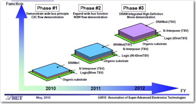
Koyanagi-san Tohoku Univ went over the Japan ASTET consortiums Dream chip program [ we have discussed this program goals about a year ago, see PFTLE 104 “3D IC From the Land of the Rising Sun” 10/30/2009] .
Koyanagi showed the ASET roadmap which shows 3D stacked DRAM memory in 2012-2013.
Phase 3 of their demonstration device shows logic mated to memory through a Si interposer in 2012.

Of great interest to IFTLE is the ASET perspective on aspect ratio. As can be seen in the figure below ASET concurs with IFTLE that mainstream TSV will have AR ~ 2:1 – 5:1 and certainly less than 10:1.
When looking at stress in 3D wafers they also use raman spectroscopy with (+) peak shifts indicating compressive stress and (-) shifts indicating tensile stress.
IMEC
Paul Marchal of IMEC examined both the yield and reliability and the electrical impact of TSV induced stress. The fig below shows the possible components of stress in the 3D structure. Their goal is to set up a simulation flow to analyze stress and its impact in a packaged 3D chip-stack
This stress caused by a copper TSV is radial tensile because of CTE difference between Si and Cu and tangentially compressive due to crowding of Si around TSV.
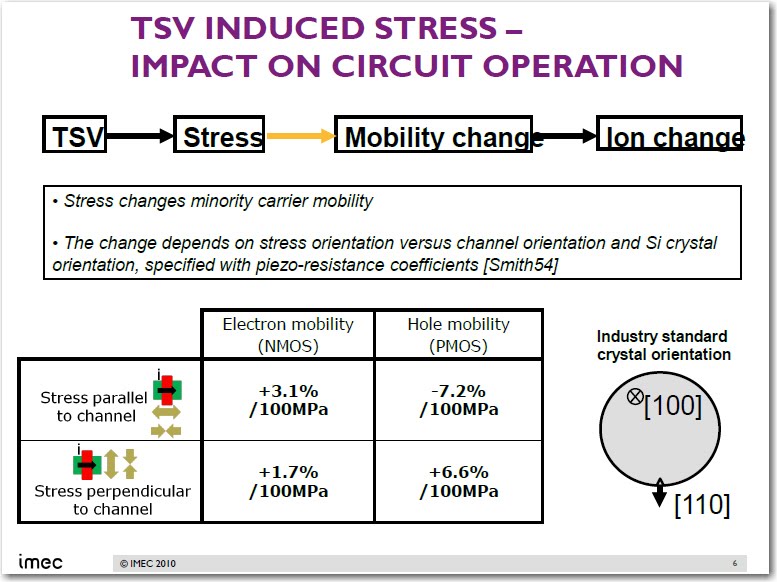
Stress impact on transistor performance is shown below:
All other things being constant, smaller TSV diameter lowers stress.
IMEC’s strategy for mitigating TSV induced stress challenges:
– Process technology optimization for TSV induced stress
– Compact mechanical model, integrated in the design flow
Remaining challenges:
– combining local and global stress
– TSV impact on advanced device topologies
Qualcomm
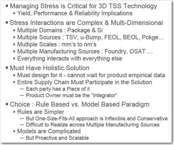
Riko Radojcic was a busy man at Semicon speaking at both the Alchimer [ see IFTLE 11 “3D in and Around the Moscone – Part 2”, Aug 2010] ] and Sematech workshops . His assessment of 3D stress risks is shown in the slide below.
His proposed solutions for managing stress are outlined below:
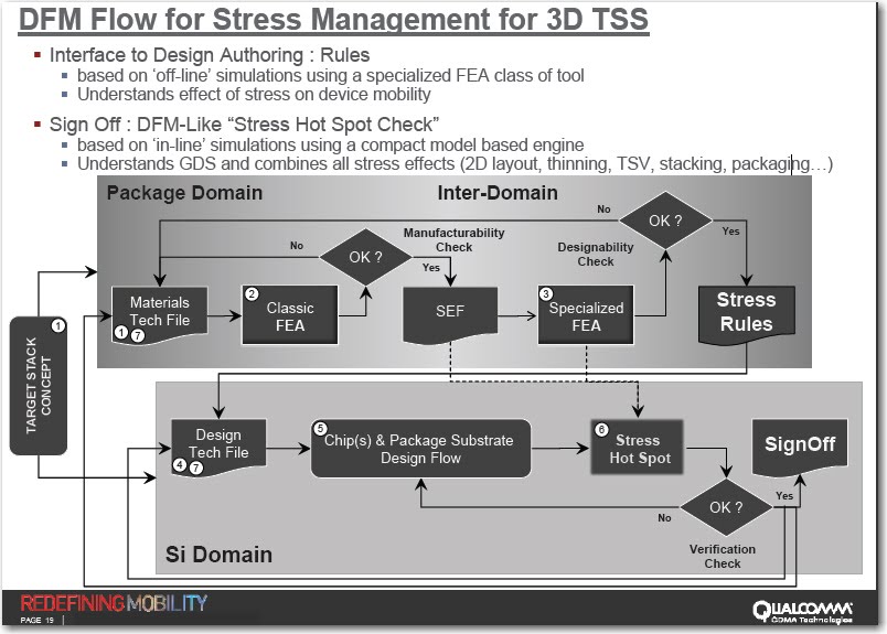
His concept of a DFM (design for manufacturing ) process flow is shown below.
Synopsis and Mentor Graphics both gave their assessment of what it will take to implement stress impact from 3Dissues into the normal design cycle. These issues were discussed in detail previously [ see IFTLE 4 “
Are we all Suffering from 3D Stress ?”, 6/2010 ]
coming soon:
– the SEMATECH metrology workshop
– the ITRS interconenct roadmap
– the ITRS assembly and packaging workshop
For all the latest in 3D ICs and advanced packaging information stay linked to IFTLEâ??¦â??¦â??¦â??¦..