
Songdong Cho, Sr engineer in the Samsung system LSI group spent the conference besieged by questions from attendees on the Samsung (memory group) announcement that occurred the day before the meeting. [see IFTLE 27, “The Era of 3D IC Has Arrived with Samsung Commercial Announcement”]
Cho first led the attendees through the evolution of Samsung 3D IC technologies:
– 2006 Samsung announces memory stacking technology
-2007 DRAM stacked memory package using TSV
-2008 TSV for CMOS image sensors mass production
– 2008 memory + logic on silicon interposer – start development
-2010 announce DRAM stacked memory with TSV commercialization
(all of these can be found in past editions of PFTLE and IFTLE)
Cho indicated that mobile products will require more than 25 GB/sec bandwidth in ~ 2012 and therefore “..wide I/O memory with TSV is the only solution” There will be two platforms for the systems LSI group: Interposer and memory on logic as shown below.


– High AR TSV filling
– Cu extrusion
– Stress impact on devices
-Copper contamination (through sidewall and during backside processing)
By eliminating voids during the plated copper filling they were able to achieve 99.57% via chain yield.
Cho lists (3) ways to deal with Cu extrusion:
– Tungsten TSV
– Cu TSV last backside
– Via size and depth reduction
They have determined a workable depth vs diameter space using the 3rd option which results in less than 0.2 um extrusion. [ recall this was first shared with us by Bob Patti – see PFTLE 53, “You Can’t Always Get What You Want”]
They worry about copper contamination when backside processing due to a decrease in the gettering layer (see previous discussions in PFTLE 117, “On copper diffusion, gettering and the denuded zone”]
Cho indicates that they will not use W because of the severe wafer bow that even 1 um of W imparts to a 300 mm wafer. They also see severe Si cracking and IMD cracking due to the high W stress.

Cho expects to see mass production from his side of the business in 2013.
Eric Beyne – IMEC
Conference co-chair Eric Beyne, program director for advanced packaging and interconnect at IMEC . The IMEC standard processes have been discussed several times previously [ see PFTLE 122, “3-D IC at the IEEE ISSCC” ; PFTLE 93, “ Semicon TechXPOTs” ]
Beyne indicates that high speed graphics applications are demanding 512 GB/sec memory bandwidth and thus agrees with the consensus that 3D with TSV is the only way to go.
The POR for their 3D TSV middle process (3D-SIC) is 5 x 50 um which looks like it is becoming an industry standard.
Their wafer thinning technology achieves a less than 1.6 um TTV for a 300 mm wafer thinned to 50 um.


Yannou focused on the use of 3D interposers for 2.5D technology and offered the following proposed interconnect gap timeline showing that silicon / glass interposers offer 10x more resolution and finer pitches than traditional organic substrates.


Arif Rahman, principle engineer at Xilinx gave further details on their next generation FPGA choices that have been reported recently [ see IFTLE 23 , “Xilinx 28 nm Multidie FPGAâ??¦”]
When asked about their choice of a silicon interposer for their next generation FPGA, Arif Rahman commented that “ it appeared to be the most manufacturable way to offer product performance during our required timeline” which I interpret as “”full 3D is not quite to the point that we were ready to bet the farm on it”
The interconnect on the interposer is done at 65 nm technology. In terms of scalability Rahman noted that the technology was currently limited by “â??¦how big an interposer you can get”
Note: After the conference Arif left word that he had moved to Altera – interesting !
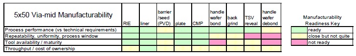
Larry Smith – Sematech
In their 3D program update, Smith indicated that after much study and consultation with its members, Sematech was focused on 5 x 50 um copper vias middle with AR = 4-10 and pitch of 10-50 um. Their status assessment is shown below:
Lisa McIlrath, CEO of R3Logic was one of the first to understand and tackle the EDA requirements of 3D IC technology. [ see PFTLE 102, “The Four Horseman of 3D IC” ]
She had what was probably the quote of the conference when she astutely stated “3D Integration will become mainstream when it is the best economic alternative” Simple yet accurate ! From her design perspective she feels that this will occur by maximizing IP re-use.
Philippe Royannez – IME
IME 3D technology has been discussed previously [see PFTLE 98, “ TSMC Confirms 3D Intent / Singapore Launches 3D IC Consortium “ ]
Philippe Royannez, Director Sytem & Digital IC at A-STAR updated activities at IME in Singapore. Royannez indicates that their 300 mm line will be fully operational n the 2nd- 3rd quarter of 2011.
In keeping with the cost reduction theme, Royannez indicated that IME “ has solutions to most of the technical challenges now. The real focus now needs to be making these solutions low cost. “
When it comes to EDA Royannez notes that “designers understand the theoretical benefits of TSV but cannot quantify it precisely and don’t quite understand what to do to use them” He notes that 3D IC EDA flow “is more evolution than revolutionâ??¦all the ingredients are there” but then quickly added “..for true 3D IC, that is the spreading of blocks across layers, certainly we’re not quite there yet, but for initial 3D programs we are in pretty good shape”
In an interesting blood pressure monitor application Royannez made the point that we need to be focused on system level integration. In this application shrinking the size of the circuits and making them faster will not have any impact on the size of the battery which will continue to drive the overall size of the device.
Tzu Kun Ku – ITRI
The ITRI Ad-STAC ( Adv Stacked system Technology and Applications) program has been detailed previously [see PFTLE 105 “Taiwanese Focus on 3D IC”]
The ITRI 3D program currently covers both chip stacking with TSV and the use of 3D interposers. There are currently 120 technologists assigned to their program (80 design, 40 process development). Their TSV formation roadmap is shown below. Their 300 mm line is in place and their baseline process is scheduled to be completed end of this year.


