Insights From Leading Edge

Yearly Archives: 2011

IFTLE 52 3D and Adv Pkging at ICEP 2011 and reschedule of 2011 3DIC (Japan)

ICEP
The ICEP [ Int Conf on Electronic Packaging] is put on by JIEP (Japan Institute for Electronic Packaging) It is usually held in April every year during cherry blossom time in Japan. I recall that in 1998,when the meeting was known as IMC/IEMT Rao Tummala and I were in attendance. At the “gala reception” we were coerced into joining the entertainment on stage and then I, as the junior member, was further coerced to dress up in a “happy coat” which my granddaughters now know as grandpa’s samuri outfit. (see below).

At this years conference, John Lau of ITRI gave an excellent invited review on the origins, status and future prospects for 3D IC which includes a must have list of 140 references in the field including his observation that Shockley, inventor of the transistor, actually patented TSV in 1958.
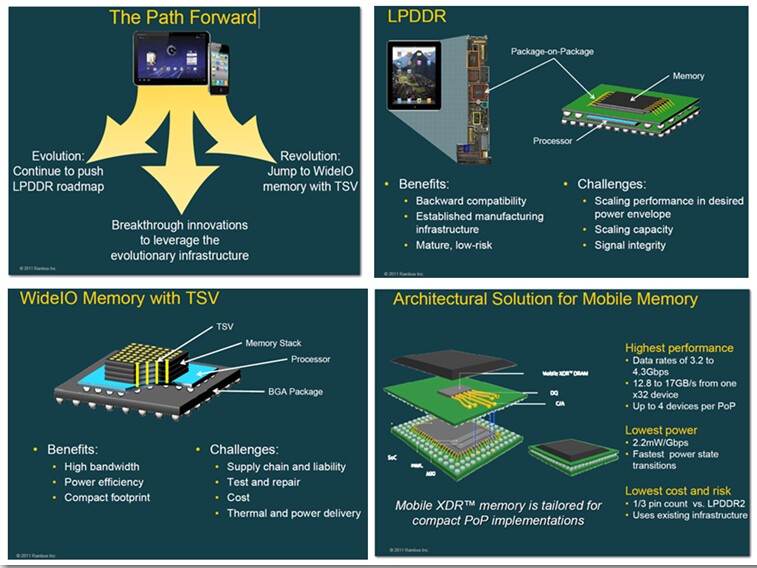
Lau astutely observes “â??¦ using a passive interposer to integrate a few “bullet proofed” chips together (like a MCM) want and are used to doing. The passive interposer becomes the most effective 3D IC integrator. It could be very low cost because we don’t have to dig and fill the holes on the active die. Also we don’t have to thin and metallize the active die. Furthermore we don’t have to temporarily bond and debond a supporting wafer to the active wafer.”
In another paper Lau and his ITRI colleagues discuss the feasibility of 3D IC for system in package structures. In their test vehicle a assive interposer supports a 4 memory chip TSV stack, an electrical test chip, a thermal test chip and a mechanical test chip to measure stress and warpage . The interposer is 12.3 x 12.2 mm and 100 um thick. The TSV diameter are 10 and 15 um on 40 And 50 um pitches.
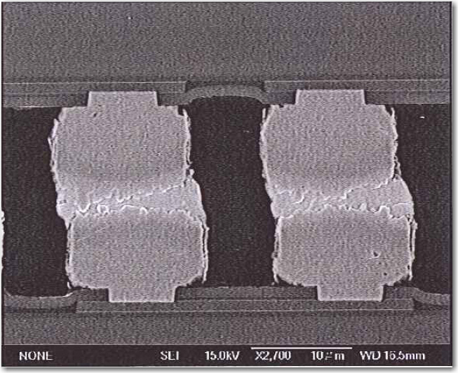
TC Chang from IRTI detailed the use of thermocompression bonding for the joining of Pb free microbumps on 20 um pitch. Solvent and plasma are used to remove the flux residue between he microgaps and a capillary underfill with 0.3 um filler (Namics) is used to fill the gaps.
NEC, Univ Tokyo and ASET reported on the formation of power regulators (buck converters) which consists of a CMOS LSI including active components and an output filter embedded in the Si interposer.
Koyanagi and co-workers at Tohoku University described their development of 5 um diameter backside TSV technology. Tohoku is located very close to the site of the Tsunami devastation so I’m sure we all wish them well as they bring their University and their 3D activities back up to speed.
To develop 5 um backside TSV the chip was supported on a glass or silicon support substrate and thinned down to 15 um by grind and CMP. ~ 1 micron SiO2 was deposited as an isolation layer / hard mask . The TSV were created with Bosch process and then lined with SiO2 (500 nm) . Etching parameters (shown below) were used to control the scallop. The bottom of the insulated TSV were opened by SiO2 etching using the thicker backside oxide layer as partially sacrificial mask for the etching.
2011 IEEE 3DIC
The IEEE 3DIC meeting which was scheduled for Tokyo this fall has been moved to Osaka in Jan 2012 due to the tsunami / nuclear disaster that Japan has been recently dealing with. The submission deadline for abstract is September 30, 2011.
For all the latest in 3DIC and advanced packaging stay linked to IFTLEâ??¦â??¦â??¦.

IFTLE 51 2011 IEEE IITC 3D Highlights, and IEEE ECTC OSAT Preview

The annual IITC, sponsored by the IEEE Electron Devices Society was held a few weeks ago in Dresden. Ehrenfried Zschech of the Fraunhofer , John Iacoponi of GLOBALFOUNDRIES and Takeshi Furusawa, of Renesas lled the program committee.
The conference which was instituted in the mid 1990’s was the premier show dealing with issues of on chip interconnect, especially low K. In recent years it has shifted some focus to 3D integration [ see PFTLE 37, “IITC on the 3D Integration Bandwagon” and IFTLE 10 IFTLE 10 “3D at the IEEE IITC”.

In this years conference Yann Civale from IMEC shared technical details on the “Thermal Stability of Copper Through Silicon Via Barriers during IC Processing”. The IMEC via-middle process flow results in several high temperature processing steps after TSV fabrication, including a final device wafer sintering step, generally in the 400°C range. As you may recall this was introduced to reduce the impact of copper extrusion [ see PFTLE 125, “ 3-D IC at Ft McDowell” and IFTLE 34 “ 3D IC at the 2010 IEDM”] Thus, it is essential to determine the stability of the TSV Cu-barrier at these temperatures to ensure a reliable integration of 3D TSV in CMOS wafers. IMEC reports that 5nm Ta barriers are thermally stable, while Ti-barriers require thicknesses above 5nm to guarantee their thermal stability.

Paul Marchal of IMEC presented a “Technology Roadmap and Status” for 3D IC. Marchal indicates that 3DIC technology is now becoming available, that co-optimization of design and procfess technology are required and that one of the remaining hurdles remains mechanical and thermal stress.

The thermo and Thermomechanical challenges for DRAM on Logic are shown below.

Interestingly scaling of the TSV diameter will strongly reduce the KOZ (keep out zone) as shown below.

The combination of microbump and underfill has been identified as the major contributor for stress on thinned die as the shrinking underfill bends the thin die around the microbump. Agreement salso needed on exchange formats and models are required.
Projections for 2015 include:
Silicon wafer thickness : preferably 50 um and holding due to stress and thermal issues.
Microbump pitch : 20 um and decreasing for improved electrical specs
SV dia / pitch : 5-3 um / 20/10 um and decreasing dia scaling to decrease KOZ, results in AR ~ 20
Armin Klumpp Peter Ramm and co workers at Fraunhofer EMFT presented their information on  “Reliability testing and Failure Analysis of 3D Integrated Systems“. Their 3D-integrated reliability test chip is a 3-level-stack with a modular layout so several types of stacked devices can be realized, numbered type 1 – 4 with basic functions of the “Bottom”, “Middle” and “Top” layers in the figure below. The larger size of the Bottom chip allows access to the measurement pads, independent of the number of stacked layers. The medium chip having TSV’s and can be tested already in the stage of thinned silicon with the appropriate metal layers on front and back side (type 1). In combination with the bottom chip daisy chains can be realized that include TSVs and assembly pads (type 3). Medium chips with no TSVs, can be tested (type 2), to be able to distinguish between TSV and assembly pad parameters. Type 2 and type 3 are available in parallel as soon as the medium chip is assembled on the bottom one. Adding the top chip forms a three level stack (type 4) with daisy chains including TSVs and two levels of assembly pads. The medium chip serves in this case as feed through for electrical signals. The top chip shortens the electrical path to form a daisy chain consisting of at least two TSVs. The chip lay-out contains several elements including Kelvin structures, DC and RF test structures, daisy chains and TSV’s with dimensions varying from 3-50 um. 3D-integrated test chips were fabricated by application of Fraunhofer EMFT´s TSV SLID technology. The applied 3D TSV process is based on inter-metallic compound (IMC) bonding and TSV formation before stacking. For reliability testing, termal cycling (-55 C° to +150 °C) was performed and additional analysis was done by cross sectioning and plasma-FIB.
ECTC Preview
Remember when we all rushed to ECTC anticipating the latest advanced packaging presentations of IBM, Intel, Bell Labs and NEC, Hitachi and Fujitsu ? Well times have changed, and over the last two decades the pendulum has swung towards the OSATS and I think it’s fair to say that Amkor, STATSChipPAC and ASE are now producing more than their share of outstanding papers at every ECTC conference.
As an example, here is the list of papers that Akor is scheduled to present next week in Orlando.
"Cu Pillar and µ-bump Electromigration Reliability Comparison with High Pb, SnPb, and SnAg Bumps" presented by Ahmer Syed

"Advanced Coreless fcBGA Package with Embedded High-Dk Thin Film Decoupling Capacitor" presented by GaWon Kim

"Next Generation Fine Pitch Cu Pillar Technology – Enabling Next Generation Silicon Nodes" presented by Curtis Zwenger and Mark Gerber of TI

"Issues in Fatigue Life Prediction Model for Underfilled Flip Chip Bump" presented by Ahmer Syed

"Crack Initiation and Growth in WLCSP Solder Joints" presented by C.J. Berry

"A Study on an Ultra Thin PoP using Through Mold Via (TMV) Technology" presented by Akito Yoshida

"Characterization of Intermetallic Compound (IMC) Growth in Cu Wire Ball Bonding on Al Pad Metallization" by SeokHo Na

Hope to see some of you next week in Orlando. For all the latest in 3D integration and advanced packaging stay linked to Insights from the Leading Edgeâ??¦â??¦..

IFTLE 50 Words of Wisdom

50 is a big round number that means IFTLE is nearly a year old here on the SST website. From the data I’ve been shown recently, we have steadily built up readership since last spring to the point that we are now getting ~10,000 readers /month to this site. â??¦â??¦.A sincere thank you for your interest.

As you know the Insights From the Leading Edge, or IFTLE as I like to call it, focuses on 3D integration and other advanced packaging technologies. We try to keep you abreast of where and when they are introduced and what kind of impact they will have on this field of Microelectronics that we have chosen to be a part of.

I just spent my 62nd birthday with my granddaughters in Houston. This gives me the opportunity to slip in another picture of the girls which I have already explained I get to do because this is my blog.

Miss Hanna (left) and Miss Madeline (right) informed me that 62 meant I was an old man. I told them that with age came experience and with experience came wisdom so they should listen to their old grandpa. They both just giggled not having a clue what I was talking about. Certainly we all get older, but do we all get wiser ? I’ll leave that as something for you to think about.
 
On my birthday I noticed that Dr Morris Chang had a few words to say in the China Post. Chang, Chairman and founder of TSMC and winner of the 2011 IEEE medal of honor, announced that TSMC is now capable of 28 nm and is focusing on 20 nm. He also announced that Moores Law would meet its demise by 2020 at which point we simply would not be shrinking transistors any more. These were strong words from a man who runs the worlds number one IC foundry. [Link] He pointed out that in the future, more attention will be paid on packaging solutions and printed wring boards which had not yet met their physical limits. For TSMC he pointed specifically to MEMS, image sensors, photovoltaics and LEDs.
At a TSMC forum April 5th in Santa Clara Chang indicated that the PC and cell phones have been the big drivers for the IC industry but that now “ a third ‘killer app. – mobile products (smart phones and tablets)” was ruling things.

Addressing 3D, Chang indicated that TSMC has poured "significant R and D" into 3-D chips using through-silicon vias (TSVs). The company calls it as a paradigm shift called "systems-level scaling," .

Looking at the 450 mm waer question he noted that "There are still a lot of challenges for 450-mm," and that TSMC “ would build a 450-mm pilot line in the 2013-2014 time frame, followed by production in 2015-2016” with “the intercept point is 20-nm”

Some might think that these concepts were put together by his underlings who are assigned to stay on top of technology, but maybe not. Chang has always been keenly interested in both the technology and the business aspects of our semiconductor industry since his early days at MIT.
My own experience with Dr Chang came about 12 years ago when I was in Taiwan introducing BCB for redistribution and bumping. We were visiting TSMC when our host informed us that the Chairman would be joining our meeting because he wanted to understand what all the of the interest in bumping and redistribution of chips was about. He personally took us out to lunch in order to have more time to absorb technical. He explained that he knew that bumping technology was being used by the mainframe players but had recently been hearing that it was moving into consumer products. A few years later, TSMC became the first foundry to put bumping capacity in place (2001). â??¦â??¦Morris Chang – without question is a wise, old man.
Intels new “3D technology”
As if we didn’t have enough trouble explaining that 3D IC technology has nothing to do with wearing glasses to watch your new TV, some reporters in the industry are now calling the Intel;tri gate transistor a “3D chip” [link] . Actually this is not something new, Intel first announced their tri-gate structure in September 2002 and indicated that they were readying it for introduction at 32 or 22 nm, which is exactly what they are doing.
This concept here is explained very nicely by Greg Crowe [link]. “Here’s the basic idea. A transistor has power flowing through it from the source end to the drain end. The presence or absence of a current is determined by the voltage level of the gate that bridges the two. The major problem with the traditional setup involves signal loss resulting from the fact that the gate only contacts the source and drain on one surface. A tri-gate transistor has three gates that make contact on three sides at once, effectively tripling the amount of surface through which electrons can travel. This produces less data leakage and uses less power than the older design.”
Intel has indicated that this will deliver a third more processing speed, and about half as much power consumption. This means that at 22 nm Intel can pack in twice as many transistors in about the same-sized chip for the same power usage, which operate a third faster – effectively giving us about 2.5X the processing power for the same power consumption.
There are those asking how this will affect the introduction of 3D IC. Only Intel knows for sure, but I can tell you that these faster ICs will be looking to access memory even faster than they do now so my guess would be that memory on logic will be needed even more.

My previous thoughts were that TSV would show up in the 22 nm Intel "ivy bridge" [see IFTLE 38, "..of Memory CUbes and Ivy Bridges…"] with both stacked memory and interposer. We will see whether that is still true.
So thanks for your continued readership and if you continue to be interesred in 3D IC integration and other advanced packaging, stay linked to IFTLE !

IFTLE 49 Mentor 3D-IC Test Strategy; GSA Memory Conf

Before we start this weeks topic, we have some corrections to offer up from IFTLE 48:

Semi and SEMATECH Lets Get it Straight

A SEMI representative got in touch to let me know that, while SEMI and some people from SEMATECH work together on 3D-IC standards, the two organizations do not have an alliance on TSV. “Both SEMI and SEMATECH are taking key leadership roles in the discussion and promotion of standards for 3D-IC technology. SEMATECH is working with SEMI on assembling standards committees and task forces. Working with SEMI, SEMATECH’s goal is to leverage standards to head-off potential show-stoppers.”

“SEMI International Standards is very involved in 3D-IC manufacturing standards. The SEMI 3DS-IC Committee was created in late 2010, and has several activities underway in three task forces. The Inspection and Metrology Task Force is measuring the properties of TSVs, the Bonded Wafer Task Force is working on parameters for bonded wafer stacks, and the Thin Wafer Handling Task Force is developing standards for transport and storage. In addition, a new task force to address trimming of device wafers and carrier wafer dimensions is expected to start work at the 3DS-IC Committee’s next meeting on Tuesday, July 12, 2011 at SEMICON West 2011. The committee is currently chaired by Applied Materials, Qualcomm, Semilab, and SEMATECH. [link][link] and [link]

They also correctly noted that “3D Interconnect Wiki: Stress Management for TSVs” (http://wiki.sematech.org/ ) and the Wiki site (http://www.semiwiki.com/forum/f2/ ) are SEMATECH not SEMI sites.

Glad you all are paying attention, thanks for the corrections and I hope that straightens it all out.

Mentor Graphics 3D-IC Test Solution

Mentor Graphics Corporation recently announced their complete Mentor test solution for 3D-IC, Tessent® v9.4 which will be released May 2011 [link].

The Tessent MemoryBIST product provides at-speed testing of stacked memory die with support for all popular DRAM protocols, and allows memory parameters (address size, waveforms) and test algorithms to be programmed post-silicon. This allows memory BIST controllers in a logic die to handle a variety of memory die stacked on top for different product variations. The product also supports at-speed testing of memory buses, which covers both bond wires and TSV interconnects. A shared-bus capability enables test of multiple memory die on the same interconnect.

The Tessent test solution reportedly addresses the three main challenges of 3D-IC testing:
– the need for higher KGD test quality to ensure acceptable package yield
– the ability to enable comprehensive testing of all die within a packaged stack
– the ability to test all die interconnects after packaging

KGD is addressed by:

– Support for advanced fault models, including at speed testing in addition to normal “stuck-at” and bridge testing.
– Test pattern compression, which enables higher test coverage while lowering the cost of test by reducing tester memory requirements and test time.
– Hierarchical test capability, which simplifies test development and debugging, reduces test time, and allows high coverage even for complex chips, limited by I/O pin count, routing congestion, or, in the case of 3D-ICs, inter die test paths
– Integration of automatic test pattern generation (ATPG) and built in self test (BIST) techniques to achieve highest coverage at the lowest cost.

3D-IC Test Challenges After Packaging
In 3D-IC stacks, each of the die must be re-tested after the die have been packaged to make sure they remain fully functional. Post-package test is the first opportunity to test all the TSV or interposer connections between die for proper connectivity and at-speed performance. For processor and memory stacks, the memory bus interface logic must also be tested at full speed.
Test point access is a problem because the bottom die is the only one with direct access pins. IMEC has proposed extensions to IEEE 1149.1 (which defines standard test access points0 to allow application of tests in multi-die stacks Their TSV-based 3D test architecture requires supporting methods for routing test data through the stack, and methods to re-sequence test patterns as appropriate for the extended scan chain paths. The Tessent tool suite provides support for implementing the IMEC extensions.
Tessent ATPG and BIST test products reportedly work together to minimize test development effort and to enable parallel testing to increase test throughput.
RAMBUS
At the GSA Memory Conference last month, Sharon Holt, Sr VP at Rambus reiterated the well known position that smartphone and tablet use is increasing and will overtake standard mobile phone use in 2015.

When looking at the options for mobile memory moving forward Holt proposes that the industry could continue to evolve todays technology based on low-power DDR2; switch to the newly announced wide I/O memory interface or use the Rambus designed XDR mobile memory solution.
 JEDEC has defined a 512-bit wide interface to increase the bandwidth between memory and logic. The interface operates at a peak data transfer rate of 12.8- gigabytes per second (GB/s), which is up to four times the performance of conventional low-power memory solutions. While Samsung and others have proposed commercialization in 2012 [see IFTLE 36, “RTI ASIP 2010 Part 2 ] and Nokia has indicated that they will see wide IO memory in production in 2013 [ see IFTLE 19, “Semicon Taiwan 3D Forum Part 2” ] Holt indicated that due to the complexity and costs, TSV-based wide I/O DRAM will probably not arrive until ”the second half of the decade’’.
SanDisk
Yoram Cedar, CTO of SanDisk took a look at flash memory.
Cedar expects to see a 5X increase in flash usage in the next 3 years :
Cedar concludes that NAND scaling will need new technologies in ~ 2014 and that “3D Read/Write Memory Will Likely Be the Successor to Floating Gate NAND Flash Over The Long Term” Note 3D here does not refer to TSV technology but rather as shown below.
Penn State
Yuan Xie, long time 3D practitioner from Penn State showed that 3D should have significant cost advantages over scaling at the 32 and 22 nodes.
What are the novel architectural designs enabled by 3D integration ?
– Latency (fast interlayer interconnect)
– Bandwidth (high number of connections bw layers)
– Heterogeneous integration
– Cost benefit
What “Killer” applications could benefit from the unique features 3D can bring ?
– High-capacity memory
– Multi/many-core ?
– Exascale computing ?
Kyowin Jin – Hynix Semiconductor
Kyowin Jin, VP of Product Planning for Hynix Semiconductor looked at the use of 3d technology in the DRAM industry. 3D TSV technology offers something to the computing, the graphics and the mobile segments of the memory industry.
Jin showed a Hynix 3D roadmap that shows prototype development for 3DS-RDIMM and for 3DS-DDR3 in 2-11 and ultra wide IO development in 2013 as shown below:
For all the latest in 3D IC and advanced packaging developments stay linked to Insights From the Leading Edgeâ??¦â??¦â??¦â??¦â??¦..

IFTLE 48 SEMATECH Addresses the Reliability Impact of Stress on 3DIC

The latest SEMATECH workshop “Design for Reliability Workshop – Stress Management for 3D ICs Using Through Silicon Vias”, in collaboration with Fraunhofer IZFP, and chaired by SEMATECHS Larry Smith, was held in March in Santa Clara. The keynote by Prof Paul Ho, U Texas,“Reliability Challenges for 3D Interconnects” served as a tutorial that outlined some of the basic incremental reliability challenges associated with the 3D technology. A presentation “Cu TSV Reliability: Modeling, Test Structures and Measurement Techniques” given by Victor Moroz of Synopsys, summarized some of the experimental work done at IMEC and presented data relating the electrical effects and stress in specific 3D structures. A paper “Thermo-Mechanical Reliability of TSV Packages”, presented by Xi Liu and Suresh Sitaraman of Georgia Tech provided an overview of the 3D state of the art work at package level. Three presentations “Design For Reliability of BEoL and 3-D TSV Structures—A Joint Effort of FEA and Innovative Experimental Techniques” presented by Juergen Auersperg of Fraunhofer, “Role of Thermo-Mechanical Modeling in 3D TSV Reliability Evaluations” by Kamal Karimanal of GLOBALFOUNDRIES, and “3D IC Reliability: A New Frontier” by Raymond Wang of ASE, demonstrated the use of various FEA approaches for modeling 3D structures. The workshop goals was to examine the mechanical stress-driven failure mechanisms, associated test vehicles, and characterization and modeling methodologies which pertain to the via- middle through-silicon-via (TSV) 3D stacking technologies.

Before I take a look at some of what was presented,  I’ll reiterate that I think readers of this blog come here for 3DIC and advanced packaging insight and part of that insight is knowing the latest spots to retrieve useful information.

We have previously discussed the SEMI/ SEMATECH alliance that is in place [ see IFTLE 33 “Micron 3D Response, SEMATECH Stds, Leti 300 mmLine” ] Semi has also been developing a Wiki site where important areas in microelectronics are to be discussed [link ] From this page you can access the 3DIC tab which leads to discussions about 3DIC. In addition SEMI /SEMATECH has now started a page [link] which covers “3D Interconnect Wiki: Stress Management for TSVs”. If you get nothing else from this blog, go to these two sites and acquaint yourself with what’s available.

Paul Ho – U Texas

Ho has examined the effect of TSV scaling on keep out zone (KOZ) and concluded that the near surface stresses degrade the carrier mobility and thus define the KOZ through the piezoresistivity effect. Defining KOZ as no more than 10% decrease in mobility :

• KOZ scales with the square of TSV diameter.

• KOZ minimized at a TSV aspect ratio less than 3
• KOZ is larger for analog devices than digital devices.

• The KOZ can be significantly reduced by using annular TSV.

Victor Moroz – Synopsys / IMEC

Synopsys / IMEC made a presentation on the characterization and modeling of 3D IC with via-middle TSV. Their studies on copper fill chemistries showed that chemistry “C” had 3X the stress of two other comparable materials. This copper had a finer grain structure and showed little to no grain growth after temp cycling.

They found no significant change in TSV C-V behavior before and after thermal cycling. When measuring the minority carrier lifetime from he transient response of a MOS capacitor they saw no significant change in TSV C-V behavior before and after thermal cycling.
After proper thermal treatment to minimize “copper pumping” (copper protrusion) they found no damage to M1 or M2 above the TSV . Examining the impact of TSV generated stress on the transistor performance they found good agreement between modeling and obtained data.

When examining the impact of Cu/Sn microbumps on N-FET logic devices of dies thinned to 25 um , they found a 40% impact on NMOS current due to he underfill that was being used to reinforce the interconnect bumps. Without underfill, no impact on current was observed. The zero stress temp was found to be ~ 160 C , i.e the curing tem of the underfill (as expected). The explanation is that the shrinking underfill bends the thin die around the Cu/Sn bump generating the observed stress.
For all the latest on 3D integration and advanced packaging stay linked to Insights From the Leading Edgeâ??¦â??¦


IFTLE 47 IBM 3D Cooling, TSMC Pkging, UMC 3D Equipment, the CIS Mkt Growth

IBM water cooled 3D IC At the recent CeBIT Fair in Hanover Germany, IBM CEO Sam Palmisano presented German Chancellor Merkel with a prototype of the IBM 3D Chip Stacking Project developed at IBM Research – Zurich. Merkel asked him, "Did you take that from Intel?" Palmisano reportedly reply, "No, ours are better”.

[Merkel gets points for pushing IBMs hot button (probably unknowingly) and Palmisano gets points for a sharp response under pressure !]

German chancellor Merkel and IBM’s CEO Palmisano


Their 3D chip stacks are cooled by 50 um micro channel cooling technology . Such liquid cooling reportedly reduces power consumption or the normal cooling fans. The cooling technology was developed by IBM together with the École Polytechnique Federale de Lausanne and the ETH Zurich within the scope of the European CMOS AIC project. Dr. Bruno Michel manages the Advanced Thermal Packaging group at IBM Research – Zurich. The group has pioneered energy-efficient hot-water-cooling and the concept of a zero-emission data center.


The first goal is reportedly to directly stack memory onto the processor. IBM’s 3D technology is reportedly scheduled to appear in its upcoming Power8 processor, planned for 2013, using 28 or 22nm process technology. While the technology is reportedly being transferred to iDataPlex servers, it is expected that it will be a few more years before it is fully ready for production.

TSMC Interposer Production in 2012, Making Move into Advanced Packaging

We first started tracking TSMC’s San Jose spring technical symposium in 2008 when TSVs first appeared on their roadmap [ see PFTLE 30, “Foundry TSVs Are a Comin’ – TSMC Makes Their Play for a Bigger Portion of the Pie” In 2009 they reconfirmed their plans for fab based TSV . [ see PFTLE 73, “ TSMC Reconfirms Plans for Fab-Based TSV “]. At this years meeting, last week, Sr VP of R and D Shang-Yi Chiang indicated that they would initially offer silicon interposer technology, which they are currently sampling and plan to have in full production by late 2012.


Perhaps more interestingly, TSMC updated the audience on a theme they first brought up in 2008 when they suggested that they might “in the future” be after a bigger portion of the packaging pie. We recently reported that TSMC would enter the interposer technology and that in fact they were delivering the interposers to Amkor for assembly already bumped, rather than have Amkor do the bumping [ see IFTLE 43, “IMAPS Device Packaging Hilights – 3DIC”] TSMC first put in bumping capacity for 200 mm wafers in 2001 when they installed 15K wafers/mo capacity for business with Altera. They have had limited bumping and WLP capacity since then although they have mainly used their OSAT partners for such operations.


Now TSMC is expanding its bumping efforts. They will ramp up a new 200,000 to 250,000 wafers per month bumping facility in Tainan, are qualifying 100-micron bump pitch lead-free and new copper pillar bump technology at the 28-nm node and are ramping up 28 nm WLP qualification by December targeting the mobile market. Although claiming to still be a “front end company” it is clear to IFTLE that TSMC is making inroads into the packaging business.


UMC Announces 3D Equipment Aquisition


In mid 2010 UMC announced their 3DIC alliance program with Elpida and Powertech Technology (PTI). [see IFTLE 8, “3D Infrastructure Announcements and Rumors” ]At that time, UMCs CTO reported that they expected to be sampling 3D IC solutrions using their 28 nm technology “..in mid 2011) with production slated for 2012. In keeping with these previous announcements, UMC has just announced that they have acquired $19 MM worth of 3D TSV production equipment from Hong Bao Technology (a 73% owned subsidiary)


CMOS image sensors continue to overtake CCD


i-Supply reports that in 2011 CIS ( a key applications area for TSV and in the future 3D IC stacking) will surpasses CCD by > 10:1 in both units and revenue.

Image sensor Shimpents and Revenue (i-Supply)


CMOS image sensors for digital cameras, the last bastion of CCD technology, are expected to exceed those of CCD devices in 2013. CMOS sensor advantages include lower power consumption, reduced cost and circuit integration. The lower power consumption of CMOS sensors yields longer battery life. CMOS sensors also allow for the possible inclusion of on-chip peripheral circuits, increasing the integration of electronics and reducing the size of DSCs. CMOS sensors also support backside illumination technology (BSI), enabling better quality imaging in low lighting conditions.


CMOS image sensors shipments for DCS are projected reach ~ 71 MM units, up from ~ 30MM in 2010. CCD shipments are expected to decline to ~ 67 million units in 2013, down from ~ 94MM in 2010. By 2014, more than 85MM CMOS are expected compared to 51MM for CCD.

Digital still camera image sensor unit shipments by technology (MM of units).


For all the latest in 3DIC and advanced packaging, stay linked to IFTLEâ??¦â??¦â??¦â??¦â??¦â??¦â??¦â??¦â??¦..


IFTLE 46 3DIC at DATE 2011; Intelâ????s Paniccia Points to Optical Interconnect ; Applied Continues Move into Packaging

DATE (Design, Automation, Test ��? Europe) was held in Grenoble Fr March 14-18.


Penn State
Yuan Xie from Penn State and IBM collaborators from the System and Technology Group took a look at 3D IC thermally-aware bus optimization.
Given that :
– TSVs are clustered for both signal and power delivery
– TSVs are duplicated (redundancy as high as 20x) for higher reliability and higher yield
What is the impact of these TSV clusters on 3D thermal profile ?

They found that large copper TSVs improve the vertical heat dissipation whereas dense and insulated tungsten via farms act as lateral thermal blockage. With the proposed TSV bus optimization flow the peak temperature can be reduced as much as 18.5K and the average temperature reduced by 4.3K.
Technology Design Forum 

The Tech Design Forum ( formerly EDA Tech Forum), has been restructured to focus on fast-growing technology markets in specific regions and has added panel discussions of industry and media experts, as well as technical sessions. They will hold the following meetings in 2011:


March 10 – Santa Clara; April 11 – Tel Avivl; July 20 – New Delhi; July 22 – Bangalore; August 25 – Tokyo; August 31 – Shanghai; September 6 – Beijing; September 8 – Hsin-Chu; September 8 – Santa Clara.


The March 10th Tech Design Forum "EDA Edition" focused on IC Design and Verification, exploring ecosystem networking and increasing competiveness in IC and system product development. The keynote by Dr. Mario Paniccia, Intel Fellow, titled "Bridging Photonics and Computing" discussed recent advances in silicon photonics, including the first silicon photonics optical link operating at 50 Gbps, the scalability of this technology and its potential applications.


Intel asks the question ��?With all the data that is moving and will need to be moved, how do we connect all these devices?

Paniccia claims that copper is approaching its limits and that optical transfer, which is now mainly used for longer distances, needs to be driven to higher volumes and lower costs to offer a solution for this market .

They feel this will be achieved first by integrating all the devices on to silicon and then by creating monolithically on a silicon base.
Applied Continues Move Into Advanced Packaging


We have previously discussed what appears to be the planned move of Applied Materials into the IC packaging space [ see PFTLE 72, ��?Samsung 3-D ��?Roadmap��? That Isn��?t��?; PFTLE 41, ��?3D Integration Stays HOT at Semicon West��? ]


Applied Materials has now signed an agreement with Singapore��?s Institute of Microelectronics (IME) to set up a Center of Excellence in Advanced Packaging in Singapore. The Center, to be located at Singapore��?s Science Park II, will focus on new capabilities in advanced packaging. When finished, this advanced semiconductor packaging RandD facility will enable IME to support Applied Materials��? product development initiatives. The Centre will have a full 300 mm line of Wafer Level Packaging (WLP) and 3DIC processing equipment and will conduct research in semiconductor hardware, process, and device structures.


Applied expects many advanced logic devices at the 40nm and below technology nodes to be packaged at the wafer level. Russell Tham, Regional President – South East Asia, said, âÂ??Â??This collaboration is to âÂ??¦. (bring) our development activities closer to our customers in Asia.âÂ??Â??

For all the latest in 3D IC and advanced packaging stay linked to IFTLE……


IFTLE 46 3DIC at DATE 2011; Intel’s Paniccia Points to Optical Interconnect ; Applied Continues Move into Packaging

DATE (Design, Automation, Test – Europe) was held in Grenoble Fr March 14-18.


Penn State
Yuan Xie from Penn State and IBM collaborators from the System and Technology Group took a look at 3D IC thermally-aware bus optimization.
Given that :
– TSVs are clustered for both signal and power delivery
– TSVs are duplicated (redundancy as high as 20x) for higher reliability and higher yield
What is the impact of these TSV clusters on 3D thermal profile ?

They found that large copper TSVs improve the vertical heat dissipation whereas dense and insulated tungsten via farms act as lateral thermal blockage. With the proposed TSV bus optimization flow the peak temperature can be reduced as much as 18.5K and the average temperature reduced by 4.3K.
Technology Design Forum 

The Tech Design Forum ( formerly EDA Tech Forum), has been restructured to focus on fast-growing technology markets in specific regions and has added panel discussions of industry and media experts, as well as technical sessions. They will hold the following meetings in 2011:


March 10 – Santa Clara; April 11 – Tel Avivl; July 20 – New Delhi; July 22 – Bangalore; August 25 – Tokyo; August 31 – Shanghai; September 6 – Beijing; September 8 – Hsin-Chu; September 8 – Santa Clara.


The March 10th Tech Design Forum "EDA Edition" focused on IC Design and Verification, exploring ecosystem networking and increasing competiveness in IC and system product development. The keynote by Dr. Mario Paniccia, Intel Fellow, titled "Bridging Photonics and Computing" discussed recent advances in silicon photonics, including the first silicon photonics optical link operating at 50 Gbps, the scalability of this technology and its potential applications.


Intel asks the question “With all the data that is moving and will need to be moved, how do we connect all these devices?

Paniccia claims that copper is approaching its limits and that optical transfer, which is now mainly used for longer distances, needs to be driven to higher volumes and lower costs to offer a solution for this market .

They feel this will be achieved first by integrating all the devices on to silicon and then by creating monolithically on a silicon base.
Applied Continues Move Into Advanced Packaging


We have previously discussed what appears to be the planned move of Applied Materials into the IC packaging space [ see PFTLE 72, “Samsung 3-D ‘Roadmap’ That Isn’t”; PFTLE 41, “3D Integration Stays HOT at Semicon West” ]


Applied Materials has now signed an agreement with Singapore’s Institute of Microelectronics (IME) to set up a Center of Excellence in Advanced Packaging in Singapore. The Center, to be located at Singapore’s Science Park II, will focus on new capabilities in advanced packaging. When finished, this advanced semiconductor packaging RandD facility will enable IME to support Applied Materials’ product development initiatives. The Centre will have a full 300 mm line of Wafer Level Packaging (WLP) and 3DIC processing equipment and will conduct research in semiconductor hardware, process, and device structures.


Applied expects many advanced logic devices at the 40nm and below technology nodes to be packaged at the wafer level. Russell Tham, Regional President – South East Asia, said, “This collaboration is to â??¦. (bring) our development activities closer to our customers in Asia.”

For all the latest in 3D IC and advanced packaging stay linked to IFTLE……


IFTLE 45 Interconnect Giants

I recently read of the passing of Dimitry Grabbe and it saddened me deeply. As time passes those that preceded us are often forgotten and their accomplishments overlooked.


The Grabbe obituary indicated that he was 83 and had most recently taught at Worchester Polytech in Mass. He was responsible for more than 500 patents in the areas of machine design, semiconductor packaging, electronics assembly and optoelectronic connector design. Dimitry joined AMP in 1973. He was recognized by AMP with a Lifetime Achievement Award, and by the American Society of Mechanical Engineers, which chose him for its Leonardo da Vinci Award. An IEEE Life Fellow, Grabbe was also a fellow of IMAPS.
In 2007 Grabbe was the fifth recipient of the IEEE Components, Packaging, and Manufacturing Technology award. His citation reads: "For contributions to the fields of electrical/electronic connector technology, and development of multi-layer printed wiring boards."


Dimitry was part of the group Microelectronic Interconnect Greats that lived in the greater NYC metropolitan area in the days before Silicon Valley. When I was still young and impressionable, Dimitry was already a highly respected “leader of the Pack” along with close friends Jack Balde of ATT (who passed away in 2003) and George Messner of AMP AKZO (who passed away in 1996). With Bell Labs in its “hey day” and IBM Yorktown up the river, some would say that metropolitan New York was the center of the microelectronics universe.


What separated these three from the rest of the professionals in the area was that they always had time for discussions with younger colleagues like myself. They understood their responsibility to set up and lead meetings on the topics of the day and to help generate the next generation of technical leaders. They were true scientists who had little respect for “managers” and were always ready to share information with all those who would listen. If there was a rumor anywhere in the industry they knew it !


Some of the greatest meetings I ever went to were local meetings held at the old IEEE headquarters near the UN building in NYC . Grabbe and Messner and Balde were always there learning new things and sharing what they knew. A native New Yorker myself, I was living in Boston at the time and would make up excuses to get to NY to attend these meetings and be around these giants. Grabbe kept a museum of electronic products in his barn in PA. Supposedly he had things in there that no other museum had. Professionals from all over the country were sending him electronic devices knowing that he would take care of them in his personal “museum”. I truly hope all of that has not been lost ! Maybe an IEEE museum in his name would be appropriate? Many colleagues knew that both Messner and Grabbe had immigrated from the old Soviet Union after WWII. Grabbe related to me many times that he had had some problems with the KGB and spent the rest of his life “packing” â??¦not packagingâ??¦but "packing" in the urban context of carrying a handgun in a shoulder holster. For those who did not know this – it was the reason he always kept his jacket on !


In the early 1992 I got the opportunity to edit the first MCM textbook “Thin Film Multichip Modules” with Messner, Balde and Motorolas Iwona Turlik. A great learning experience on how to assemble and share information. (Little did I know what I would be doing later in life)

A young Garrou, Iwona Turlik (Motorola), Messner and Balde at the publication of the book Thin Film Mltichip Modules


Grabbe and Balde also share the fact that they have received the IEEE CPMT Society medal, the highest honor available for packaging and interconnect practitioners. It’s worth looking at the list of winners of this award since these are truly the giants in our packaging field.


2004 – Jack Balde – ATT


2005 – Yutaka Tsukada – IBM


2006 – C. P. Wong – ATT, Ga Tech


2007 – Dimitry Grabbe – AMP


2008 – Paul Totta, Karl Puttlitz – IBM


2009 – George Harman – NIST


2010 – Herbert Reichl – Fraunhofer IZM, Berlin


2011 – Rao Tummala – IBM, Ga Tech


If anyone reading this does not know who these men are or why they won these awardsâ??¦well you’ve got some reading to do !


For all the latest on advanced packaging and 3D IC technology stay linked to IFTLEâ??¦

IFTLE 44 JEDEC Standards, Hynix moves on 3DIC and IC Power Rankings

JEDEC ANNOUNCES 3D-IC STANDARDS DEVELOPMENT
JEDEC has recently summarized their ongoing standards development work related to 3D-ICs. The following JEDEC committees and task groups are engaged in developing 3D-IC standards:
Memory:
– the Solid State Memories Committee (JC-42) has been working since 2008 on definitions of standardized 3D memory stacks for DDR3 . Future DDR4 standards will be implemented with 3D input.
– the Multiple Chip Packages Committee (JC-63) is currently developing mixed technology, pad sequence and device package standards.
– a Low Power Memories Subcommittee (JC-42.6) task group is developing standards for Wide I/O Mobile Memory with TSV interconnect stacked on SoC Processors.
Quality
and Reliability
:

– the Silicon Devices Reliability Qualification and Monitoring Subcommittee (JC-14.3) is working on reliability interactions of 3D stacks and has released JEP158: 3D Chip Stack with Through-Silicon Vias (TSVS): Identifying, Understanding and Evaluating Reliability Interactions.
– reliability test methods developed by JC-14.1 and JC-14.2 and quality documents developed by JC-14.4 are applicable to 3D-IC packaged and unpackaged evaluations and qualifications.
Packaging :
– the Mechanical Standardization Committee (JC-11) has been working since 2010 on Wide I/O Mobile Memory package outline standardization, including a task group focused on design guide creation.
JEDEC invites interested companies and organizations to participate.
I have previously expressed my concerns over the lack of transparency in JEDEC standards due to their self imposed rule forbidding revealing authorship [companies and /or individuals] up the standards. [ see PFTLE 128 “3D IC Standardizatio Begins” ] Those concerns still stand.

Hynix Semiconductor Joins SEMATECH’s 3D Interconnect Program
Hynix the last top 5 DRAM to not have announce plans for 3D IC has become a member of SEMATECH’s 3D Interconnect program. Dr. Sung Joo Hong, Head of the R and D Division of Hynix Semiconductor commented that "3D integration offers a path for higher performance, higher density, higher functionality, smaller form factor, and potential cost reduction,â??¦.by joining SEMATECH’s 3D Interconnect program and collaborating with industry-leading partners, we expect to play a critical role in accelerating the commercialization of wide I/O DRAMâ??¦” Hong reported that Hynix and SEMATECH will address the commercialization challenges facing the industry as it commercializes wide I/O interface structures using TSVs in high volume manufacturing in the next two years.Hynix will be working with IBM, GlobalFoundries, Toshiba, Samsung, Applied Materials, Tokyo Electron, ASML and Novellus as part of the SEMATECH program.

IC Power Rankings from IC Insights


Semiconductor industry capital spending is becoming more concentrated, with a greater percentage of spending coming from a shrinking number of companies. As a result, IC industry capacity is also becoming more concentrated, and this trend is especially prevalent in 300mm wafer technology.


IC Insights has created a “Power Rating” which is determined by each company’s 300mm wafer capacity and its rank in capital spending.

Overall, IC Insights believes that the top-10 companies in the “Power” ranking will be the primary drivers in adding capacity over the next few years. GlobalFoundries and TSMC get a boost from their currently aggressive capital spending plans and are very likely to add a significant amount of 300mm capacity over the next few years. Among companies ranked between 11 through 22 Renesas, IBM, TI, ST, and Fujitsu are moving to or continuing with a fab-lite strategy. These five companies appear unlikely to add new 300mm capacity in the future. Powerchip, SMIC, ProMOS, Winbond, and Xinxin appear limited by financial where-with-all (e.g.,) or a lack of desire (e.g., Rohm and Panasonic) to add significant amounts of 300mm capacity to produce leading-edge digital ICs.


With only ten major players in the 300mm capacity space, the customer base for leading-edge IC production equipment has become very narrow. It is likely that IC equipment and materials suppliers will be focused on these 10 companies in the future.


For all the latest in 3DIC and advanced packaging news and conference updates stay linked to IFTLEâ??¦