Insights From Leading Edge

Yearly Archives: 2011

IFTLE 43 IMAPS Device Packaging Highlights – 3DIC

Ft McDowell AZ was once again the site of the IMAPS Global Business Council Meeting and Device Packaging Conference. For a report on last years conference see PFTLE 123,125,126 [link]


Brandon Prior of Prismark Partners pointed out that 3D TSV will be competing with the incumbent mobile phone 3D packaging solutions, PoP and PiP. PoP lacks the ability to interconnect more than 200 – 300 I/O from memory, but offers ease of test. TSV will offer higher speed and many more connections .


James Malatesta of Micron presented his perspective on the work of JEDEC committee JC63, the multichip package committee. First PoP changed the landscape as logic suppliers realized that standard top package “memory modules” were requuired for multiple industry supply sources. He also gave an interesting comparison of low power DDR2 [LPDDR2] vs the wide IO TSV technology that is expected to replace it [see IFTLE 40, “Samsung Wide I/O DRAM for Mobile Productsâ??¦”]

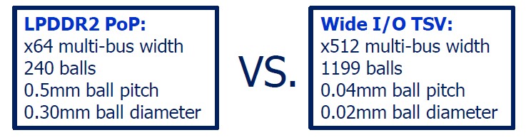
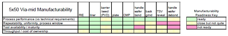
Sitaram Arkalgud, Director of Sematechs 3D IC program described their current acivities on the U Albany campus. They view their role as helping to :

• Develop robust technology solutions
• Assist member company implementation
• Drive convergence of the materials/equipment solutions


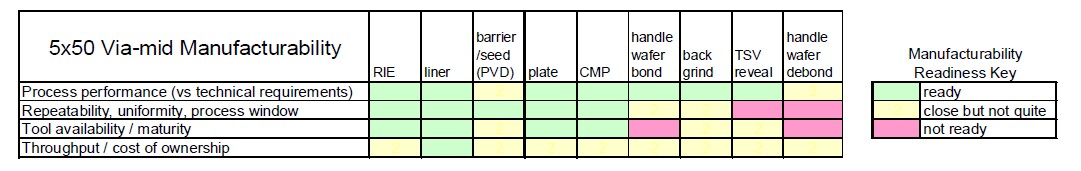
Sematech has examined the current 3D TSV tool set and come to the following conclusions:

Rosalia Beica of Applied Materials announced that EMC 3D has achieved their goal of less than $150 / Wafer for 3D processing.

In Matt Nowak, Sr Director at Qualcomm, presentation he asked the question “since the key attributes of 3D IC are: (1)Performance enhancement; (2) Improved power efficiency; (3) Form factor miniaturization and (4) Cost reduction can 3D IC take the place of scaling as CMOS technology appears to be slowing down or stalling out” . He concludes:

• If performance enhancement and power reduction are the primary motivation, then TSS opens new opportunities for innovative architectural and SW solutions with major improvements possible. But requires Pathfinding and risk taking.
• If form factor miniaturization is the only motivation, then yes
•If cost reduction is the primary motivation, then generally the answer is no. However, TSS can provide cost reduction within a window of time for large die sizes on leading edge nodes.
• If cost improvement from CMOS scaling diminishes in future nodes (due to Adv Litho and FEOL cost), then the window of opportunity for TSS increases.


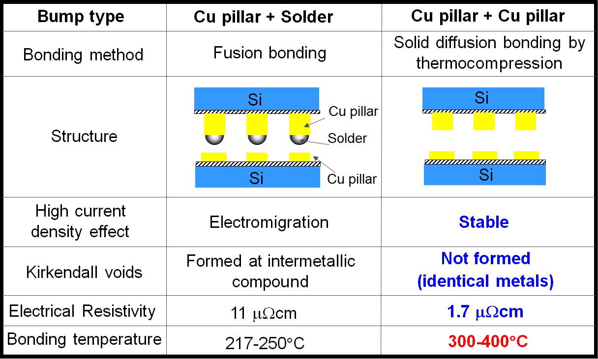
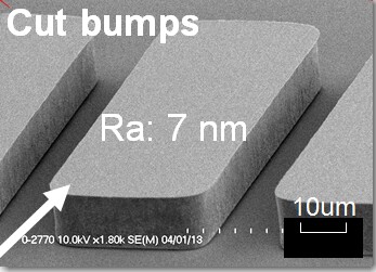
Taiji Sakai of Fujitsu made a strong case for why low pitch bonding has moved to copper pillar bumps and wants to move to direct Cu-Cu bonding . The limiting factor preventing that move right now is time/temp required.

Sakai reports that if the Cu bumps are cut (planed) with a diamond bit a surface Ra of 7 nm is obtained and an “amorphous like layer” is produced at the surface. Forming a monolithic interface is possible at 200 – 250C (30 min) vs the 350C (30 min) required for a CMP’ed surface.
3D Panel Session

The 3D panel session was put together by Qualcomm’s Matt Nowak and moderated by Applied Materials Paul Siblerud.

Interposers failing thermal cycling tests


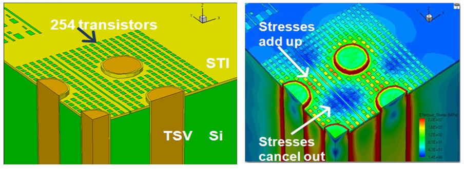
It was the fall of 2009 that everyone became aware of copper protrusion (or pumping ) as a reliability issue in 3DIC technology. This was discssed extensively in last years IMAPS DPC[ see PFTLE 125, "3D IC at Ft McDowell"] . In the last 12 months many major players confirmed the issue, solutions were proposed and our fears were allayed as to this being a showstopper for 3D IC technology [see IFTLE 6, "Cu-Cu and IMC Bonding Studies at 2010 ECTC"; IFTLE 30, "IEEE 3DIC 2010 in Munich" and IFTLE 34, "3D IC at the 2010 IEDM" ].


The rumors going around at this years IMAPS-DPC were concerned with interposers reportedly failing thermal cycling (TC) reliability tests. Word has it that when the interposers are populated with unequal size or thickness silicon chips or stacks the stresses generated on the interposers is so significant that it causes interposer fracture. I asked the panel, which I was part of, to comment on these rumors. Ron Huemoeller, VP of 3D packaging for Amkor answered that this indeed was the case, that they had seen such problems in the Xilinx scaleup. The good news from Ron is that they were able to engineer around these issues. FYI, recall that the Xilinx interposer is 100 um thick. It is unclear from the current rumors at what thicknesses (chips, stacks and interposers) these issues are seen.


Underfill with Interposers


Underfill has been around since Tsukada told us that they allowed bumped chips to reliably be used on laminate substrates back in 1992. Thus, one would think that underfills would not crop up as a problem in todays 3D technology. However, you must recall that for something like the Xilinx structure [see IFTLE 28, "Xilinx 28 nm Multidie FPGA..." we are talking about microbumps on 45 um pitch, not your typical 150 um solder bumps on 400 um pitch. Amkors Huemoeller comments on the 3D panel that the underfill process took a year get to a manufacturable state. Hopefully the underfill supplies now have the formulations set and can recommend solutions that can be implemented much quicker than that.

Phil Garrou (representing Yole Developpment), Ron Huemoeller (Amkor) Eric Strid (Cascade Microtech), Matt Nowak (Qualcomm), moderator Paul Siblerud (Applied Materials)

EMC 3D closing downâ??¦â??¦.


Paul Siblerud of Applied Materials gave the conference pre notification that EMCD 3D consortium members have concluded that they have met their goals and will be closing this summer. Their last presentation as a group is expected to be at Semicon this July.

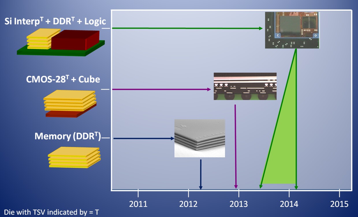
Memory Stack Usage coming soon
Huemoeller offered the following Amkor roadmap for memory stack usage:

 Representing Yole Developpment I offered the following slide as representing the major 3D IC announcements in the past 12 months.

And the following chart to summarize active major players and their expected timelines for interposer and stack introductions.

The Latest on Xilinx FPGA Production with TSV Based Interposers

At the GBC, Suresh Ramalingam of Xilinx discussed the key role of supply chain collaboration. The FPGA is basically a programmable SoC of logic, memory and analog circuits.

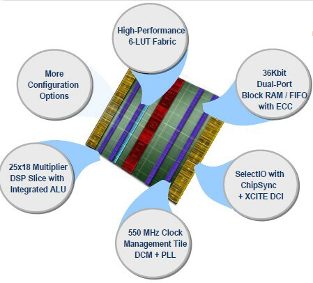
Customers were asking for more logic capacity, more high speed transceivers, more processing elements and more memory and Xilinx was faced with the reality that yield of the devices is directly proportional to device size. Rather than try to interconnect smaller devices on a PWB or MCM, which did not offer enough I/O and resulted in high latency and high power usage, their preferred solution was to connect FPGA “slices” on a silicon interposer which offered massive low latency interconnect (10K routing connections between slices with ~ 1ns latency) and low power consumption. They claim this gives them a 1.9X advantage over their nearest competitor.

The 28nm Virtex-7 SSIT will reportedly use TSMC fabricated 100µm thick silicon interposers with 10 – 12 µm Cu TSV and 65nm interconnect. The micro-bumps are Cu-SnAg alloys at 45µm pitch.


The supply chain they put together includes TSMC, Ibiden and Amkor as shown below.

Mike Kelley, Sr Dir of Advanced 3D Packaging for Amkor indicated that Amkor bumped the FPGA chip wafers whereas the interposers from TSMC arrived bumped and ready for assembly.


Amkor offered the following process flow for test during assembly :

For all the latest in 3DIC and advanced packaging news stay linked to IFTLE………….


IFTLE 42 IMAPS Device Packaging Conference – Fan Out and Embedded Packaging

Ft. McDowell AZ was once again the site of the annual IMAPS Global Business Council Meeting and Device Packaging Conference. [For reports on last years conference see PFTLE 123,125,126]

Fan out and Embedded Packaging

Andy Strandjord and Linda Ball put on an excellent panel session on fan out and embedded technology.

John Hunt (ASE), moderator Linda Ball (Freescale), moderator Andy Strandjord (Pac Tech), Thorstern Meyer (Intel Wireless [formerly Infineon]),Tom Strothman (STATSChipPAC), Lars Boettcher (Fraunhofer IZM), Navjot Chhabra (Freescale)

Thorsten Meyer one of the developers of the Ifineon eWLB fan out technology informed the audience that his group is now part of the Intel purchase of the Infineon wireless business. They are now the stand alone business “Intel Mobile Communications” Infineon retains rights to non wireless applications. Anyone wanting to license the technology moving forward will have to license from both parties.

Navjot Chhabra (recently from the Sematech ultra lowK program) is now Director of the Freescale RCP fanout technology. They are currently running a 200 mm engineering line while licensee Nepes has a 30 mm line running in Singapore. [see IFTLE 25, “IMAPS Part 2: Advanced Packaging] He indicates that qualifications for “â??¦industrial and automotive products are ongoing”

Meyer also reveled that IZM had licensed their embedding technology (shown below) to Infineon.

Tom Strothman of STATSChipPAC indicated that eWLB is today less costly than FcBGA. STATS is currently running a 300 mm line for production of eWLB.

The panel made the interesting comment that both the fan out and embedded technologies were capable of 0.3 mm pitch but that drop test reliability would go down because the UBM cross section would be smaller.

John Hunt of ASE indicated that ASE does not have 300 mm eWLB in production but commented that “..demand just does not warrant putting that capacity in place” . It was news to me, and I’m sure it will be to most of you, that Infineon is the only commercial customer for eWLB today. Reportedly ST Micro is close but today it is only Infineon .

Much has been made of the possibility for eWLB to move to panel production. Having tried to do thin film packaging on 450 mm panels at Micromodule Systems in the mid 90’s (see fig below) I know that this is easier said than done. (FYI that’s AVX’s Bob Heistand 3rd from the left on top row, Intels Mike Skinner to the right of me and Larry Moresco in front of him. MMS program Mgr Chung Ho was absent from the
picture.

While all of the eWLB licensees are proposing fan out packaging on panels Hunt commented that “â??¦we (ASE) are actually the only ones who have tried to do thisâ??¦.If we move forward with this approach it will require a totally new materials set” Hunt also indicated that they are attempting this work on ¼ panels not full PWB panels and obviously they cannot use MUF (molded underfill) to encapsulate the large substrates.

Next week we will look at a summary of 3D activity at the IMAPS DPC

For all the latest in 3DIC and advanced packaging information stay linked to Insights from the Leading Edgeâ??¦.


IFTLE 41 SRC Focus Center 3D Update

Founded in 1998, the Focus Center Research Program (FCRP), is one of three research program categories of the well known Semiconductor Research Corporation (SRC) [link]. FCRP research is always looking long-term and big-picture, seeking breakthroughs that are “critical to U. S. security and economic competitiveness”. FCRP programs involve 41 universities, 333 faculty and 1215 doctoral graduate students. The Focus Centers themselves are not physical locations, but rather consist of multiple universities which engage the leading experts at the participating institutions. Each Center is managed by Center Director and addresses one of the major technology focus areas of the International Technology Roadmap for Semiconductors (ITRS).
The SRC runs 6 “focus centers” (below). All 6 centers believe 3D is important and are working in the area. On Feb 11th the first cross center 3-D workshop was held.

Tanay Karnik of Intel examined 3Dintegration from the perspective of a processor company. IFTLE has discussed the requirements for low power high bandwidth memory in several recent blogs [ see IFTLE 38, “of memory cubes and Ivy Bridges” and IFTLE 40, “Samsung Wide I/O DRAM for Mobile Productsâ??¦”]. The slide below shows the bandwidth required to stay on the roadmap.

When examining thermal issues Karnik emphasized that thermal floorplanning was necessary to insure that thermal hot spots are not aligned as shown below.

In addition thermal TSV will likely be needed to carry heat directly to the heat spreader as shown below.
Jerry Bartley of IBM 3D opportunities and prerequisites to deployment. Bartley gave the following standard IBM list as 3D IC advantages:
Bartley sees an evolutionary path whereby the via diameter, via pitch, number of layers, complexity of the layers, will systematically improve with time. As we have repeatedly said here at IFTLE, Bartley sees “â??¦3D adoption within any application will happen as the technical risks are mitigated and clear cost and performance advantages emerge”

In agreement with Intels Karnik, Bartley points towards to thermal awareness as a necessary prerequisite for 3D design as shown below.

Bartley sees 3D optimization requiring “3D thinking and system level thought processes” and lastly asks the question that a lot of us are struggling with “Is it a chip or a package ?”


Andrew Kahng of UC San Diego reviewed IRTS technology working groups which are involved with 3D technology. IFTLE has recently reviewed the same material [ see IFTLE 16, "The 2009 ITRS Roadmap.."] As an example of some of the things being looked at Kahng pointed to the prober challenges we are expected to see after 2013.


Paul Franzon from North Carolina State discussed he design of 3D systems. Franzon also identified memory on logic as a key driver for TSV based 3D architecture with examples such as high end mobile graphics synthetic aperture radar. When examining the advantages of 2D vs 3D for the synthetic aperture radar application we can see that 3D has significant advantage.
Muhannad Bakhir from Ga Tech focused on liquid cooling for high performance 3D systems. While the thermal impact of micro channel cooling can be significant, the space occupied by the liquid cooling channels is not insignificant and will limit the thinness of the strata.
For all the latest information on 3D IC and advanced packaging stay linked to Insights From the Leading Edgeâ??¦â??¦.


IFTLE 40 Samsung 3D IC Wide I/O DRAM and Semiconductor Predictions for 2011

Samsung wide I/O DRAM for Mobile Applications

Samsung, who first revealed 3D TSV stacked memory prototypes in 2006, announced 40nm 8GB RDIMM based on four-gigabit, 1.5V, 40 nm DDR3 memory chips operating at 1,333MHz and 3D TSV chip stacking technology in Dec of 2010. Samsung claimed the 3D TSV technology saves up to 40 percent of the power consumed by a conventional RDIMM and improves the memory chip density. This DRAM chip was suggested for servers to reduce power consumption and save space. They said Samsung planed to apply the higher performance and lower power features of its TSV technology to 30nm-class and finer process nodes.

At the recent plenary lecture of Dr Oh-Hyun Kwon, President of Samsung ‘s semiconductor business, at IEEE ISSCC 2011 (Int Solid State Circuits Conference), he announced the development of wide I/O 1 Gb DRAM. This memory is reportedly aimed at mobile applications like smartphones and tablet computers. Kwon reports that the 3D TSV architecture will be implemented on their 50 nm node DRAM technology. In related disclosure at the ISSCC Samsung researchers offered more details about the wide I/O memory chip in their technical presentation entitled “ A 1.2V 12.8 Gb/s 2 Gb Mobile Wide I/O DRAM with 4 x 128 I/O Using TSV Based Stacking”.
Previous generations of mobile DRAMs used a maximum of 32 pins for I/O. The new wide I/O solution which has 512 I/O (up to 1200 total) pins can transmit data at a rate of 12.8-Gbytes per second resulting in a significant improvement in processing power. In addition it reportedly reduces the power consumption by 75% by reducing load capacitance. It is expected to replace low power DDR2 DRAM (LPDDR2) which runs at approximately 3.2-Gigabytes per second according to Samsung.

Following this wide I/O DRAM launch, Samsung is aiming to provide 20nm, 4Gb wide I/O mobile DRAM sometime in 2013. Traditionally "wide" parallel interfaces have been more expensive to manufacture and package. Samsung claims, however, that its 1Gb memory chip with wide bandwidth can be installed instead of a larger amount of smaller chips which results in reduced costs and higher performance.


The die area is 64.34mm2, about a 25% increase when compared with 1Gb LPDDR2. This comes mostly from the increase in number of circuits to support 4-channel and 512-DQ feature. The whole chip is made up of 4 partitions which are symmetric with respect to the chip center, and each partition consists of 4�?64Mb arrays, peripheral circuits and microbumps. To reduce power consumption in 512b I/O operations and to support high data bandwidth, I/O driver loading is reduced by adoption of 44�?6 microbump pads per channel, which are located in the middle of the chip. The microbumps are 20�?17μm2 on 50μm pitch. A fabricated TSV has 7.5μm diameter, 0.22 to 0.24Ω resistance and 47.4fF capacitance.
Semi ISS

The SEMI ISS meeting (Industry Strategy Symposium )[link] is an annual January event in Half Moon Bay, CA where industry experts and other economic prognosticators make predictions about the upcoming year for the semiconductor industry. [ see PFTLE 121, “IC Consolidation, Node Scaling and 3D IC” for last years coverage]

Bill McClean of IC Insights pegged the 2010 semiconductor market at $313.8B, an increase of 32% over 2009. He is predicting a 10% increase for 2011. He claims a 98% increase in capex occurred between 2009 and 2010 and projects a 6% increase in 2011 to $53.8B. The semiconductor materials market saw a 24% increase between 2009 and 2010 to $42.9B and will see a 8% increase in 2011.

When looking at capex by region (2011 projected vs 2005) we see NA holding constant, Japan and Europe going down while Taiwan and Korea are going up.

10 companies held 85% of the worlds 300mm capacity in 2010.

Handel Jones of IBS predicted the following :

– 28.1% semiconductor growth in 2010 to be followed by 7.4% increase in 2011. He predicts the next downturn will be in 2013
– 32 nm is in high volume at Intel and 28 nm is ramping at the major foundries, i.e TSMC, Samsung, Globalfoundries
– Intel will ramp 22 nm in 4Q 2011, others ramping in 2012 or 2013
– process technology development is concentrated into a declining IDM and foundry vendor base
– roadmaps past 22/20 nm are unclear
– IC vendors are migrating into providing system level solutions
– A number of significant companies are making significant expenditures in 3D TSV technology with memory on package being a key driver

When looking at growth by geographic region IBS sees China becoming 50% of total consumption by 2012-2013. This means foreign supply will remain a significant portion (ca. 90%) of consumption out into he future (2015)

Reitterating his prediction of last year [ see PFTLE 121, “IC Consolidation, Node Scaling and 3D IC” for last years coverage] Jones still sees only Samsung , Intel and maybe ST Micro as IDMs with their own 22 nm logic lines. The reason for this is again explained in terms of the “cost of developing the next generation process technology” as shown below.
For the first time since we have started following the scaling roadmap, Jones sees an increase in cost / gate at the 22 node.

Thus at 28 and 22 nm taking cache off chip into a 3D technology may be a viable economic option.

For all the latest in 3D integration and advanced packaging stay linked to IFTLEâ??¦â??¦.

Hope to see many of you at the IMAPS Device Packaging Symposium in AZ next week !


IFTLE 39 Packaging Roadmaps at MEPTEC

In November of 2010 MEPTEC (Microelectronics Packaging and Test Engineering Council) : a trade association of semiconductor suppliers and manufacturers)[link] brought together a group experts from AMD, Altera, Amkor, ASE, Cisco, LSI, Micron, TechSearch, Unisem , Yole and others to discuss the status of Semiconductor Packaging Roadmaps. While the presentations themselves may have had more meat on the bone, many of the handouts were short on data and long on marketing fluff or are materials that we have already recently covered. There were, however, a couple of presentations worth looking at.


Bill Bottoms, CEO of 3MTS gave the introductory talk taking a look a collaborative roadmaps and international roadmap perspectives. From his position as chair of the ITRS (Int Technology Roadmap for Semiconductors) packaging and assembly TWG (technical working group) Bill reminded attendees that ITRS is sponsored by Europe, Japan, Korea, Taiwan and the US to:


– forcast semiconductor technology requirements 15 years out and
– forcast emerging semiconductor devices and materials 10 years out


Its relationship to other Microelectronic roadmap activities in the US is shown below where i-NEMI is actually the pivot point for all the microelectronic activities.

On a global basis, the other organization looking at overall semiconductor packaging solutions is JISSO [link], a Japanese term which reflects the total packaging solution for electronic products. The chart below shows its relationship to other global standards organizations.


Bottoms premise is that for the past 40 years semiconductor progress could be easily predicted. The focus was on design and fab. Semiconductor roadmap goals were all clearly focused on shrinking geometries (scaling) and increasing wafer size. However, as we enter the “deep submicron” era, however, things become more complicated and packaging becomes a more important in delivering semiconductor yield, reliability and performance.

The answer developed to adress the historical lack of package scaling to match IC scaling was to generate the packaging at the wafer level, i.e. wafer level packaging or WLP. WLP, now firmly entrenched as a packaging option offers portable consumer products :


– inherently lower cost
– better electrical performance
– lower power requirements
– smaller size


Several architectural variations of WLP are in use today as are shown below.

Another important trend in packaging is the incorporation of multiple die into a single package or what has become known as System in Package (SiP) [ MCM to those of us that have been around awhile].
Moving forward, Bottoms predicts, as many of us do, that the 3rd dimension will be the key enabler in maintaining the “price elastic growth of the electronics industry”. While 3D presents many challenges they all appear to have reasonable solutions. 3D will appear first through silicon interposers with through wafer connections and then through chips fabricated with internal TSV for through wafer connections .

Bill updated attendees with where the packaging roadmap would be increasing and expanding coverage in 2011. [ see “Packaging, assembly changes coming in next ITRS Update” ]

Bottoms concludes that the pace of change in packaging technology has never been greater and roadmaps are critical to continuation of this rate of progress.


Bryan Black of AMD looked at why 3D is required if semiconductor technology is to continue to move ahead. In standard fashion Black defines 3D technology in two varieties as shown below, TSV in active devices and TSV on interposers.


From a systems standpoint Black proposes the interesting perspective that performance density drives new form factors, new form factors discover new usage models and without new form factors the industry would stagnate. This trend is shown in the slide below:


For all the latest on 3D integration and advanced packaging stay linked to IFTLEâ??¦..


IFTLE 38 …of Memory Cubes and Ivy Bridges – more 3D and TSV

The 3D TSV announcements keep coming at a “fast and furious” pace and are becoming hard for all of us to keep up with. One announcement (this past week) and one rumor, are very important for the forward momentum of 3D IC integration.

A few weeks ago Mark Durcan, COO of Micron, at the IEEE ISS meeting in Half Moon Bay, commented that Micron is ”sampling products based on TSVs” and that “Mass production for TSV-based 3-D chips are slated for the next year or 18 months” [see IFTLE 33, “ Micron 3D Response, Sematech Standards, Leti 300 mm Line” ]

Now, Micron has announced that it is using TSV technology to address the longstanding problem referred to as the "memory wall". [see “Micron to reveal tech it says increases chip speed 20-fold” ]


For those that are interested, the seminal paper in the area appears to be “Hitting the Memory Wall: Implications of the Obvious” by Wulf and McKee in the March 1995 issue of Computer Architecture News which can be read here [link]. It presents an interesting discussion of the bounds on processor performance imposed by memory performance. Historically, processor performance has improved by about 60% per year, whereas the corresponding improvement in memory access time has been less than 10% per year. Latencies are dominated by DRAM access times which has changed VERY slowly over last 20 years. DRAM performance is constrained by the capacity of the data channel that sits between the memory and the processor. No matter how much faster the DRAM chip itself gets, the channel typically chokes on the capacity. Systems are not able to take advantage of new memory technologies because of this latency issue.

Brian Shirley, vice president of DRAM Solutions at Micron claims that their “hyper memory cube” technology “â??¦offers a 20-fold performance increase while reducing the size of the chip and consuming about one-tenth of the power”. They reportedly accomplish this by stacking memory on top of a controller layer (shown in the Micron fig below as logic layer) and connecting with TSV. The “wide bus” from the controller layer to the CPU is reportedly “hugh” (possible 512 bits ??)


Shirley commented “Performance needs are most dire in networking and cloud computing. One-hundred gigabit Ethernet routers and switches and cloud computing servers require everything they can getâ??¦â??¦this is our way of giving them a fire hydrant.”

They hope to see the memory cube technology in server and networking markets as early as 2012, with significant volumes in 2013, and could then start to work their way toward the consumer space in 2015.


The overall concept of the control layer reminds IFTLE of the structures that Bob Patti of Tezzaron has been showing for the past 5 years (see below)

The Intel Ivy Bridge Processor is the 22 nanometer die shrink of the 32 nanometer Sandy Bridge which is expected to be commercialized in late 2011 or early 2012. Ivy Bridge is expected to pack low-power, low-speed, but large bandwidth memory (some report up 512 bits).


Although Intel will not confirm, rumors persist that the key to Ivy Bridge’s reported performance is its stacked memory and silicon interposer [see: “Intel puts GPU memory on Ivy Bridge” ]


Rumors are that Ivy bridge will use LPDDR2 memory, possibly with a speed of only 1066MHz, and that memory stacking technology could bring it up to 1GB. The memory is then stacked upon a silicon interposer. The reason a silicon interposer is essential for Ivy Bridge is the large width of the low-power memory. Since 512 bit brings with it high pin and trace counts, which would require more layers and increase cost. The interposer decreases the required on chip layers and reducing the overall cost.


IFTLE has taken the rumors a step further. IFTLE thinks it is possible that the following patent application [ see: US 7,841,080 B2 ] entitled “Multichip Packaging using an Interposer with Through Vias” which describes having a CPU on an interposer with stacked DRAM and a voltage regulator may be related to the Ivy Bridge implementation.


Ivy Bridge may be Intel’s first product introduction with TSV. We’ll know for sure one they release the information and/or once Ivy Bridge is released and analyzed by someone like Chipworks.


One additional comment. It is likely that the use of an interposer (if true) reveals that Intel agrees with Xilinx [ see: IFTLE 23, “Xilinx 28 nm Multidie FPGAâ??¦” ] and indeed true 3D stacking (memory directly bonded to logic circuits with TSV) is not yet available and/or ready for “prime time” â??¦.yet.

For all the latest in 3D integration and advanced packaging stay linked to Insights from the Leading Edgeâ??¦.


IFTLE 37 Advanced Packaging at Singapores EPTC

Like the IEEE ESTC meeting held in Europe [see IFTLE 26 Adv.Pkging at the 2010 ESTC] , Asia’s IEEE EPTC meeting, held every year in Singapore, is a sister meeting of the IEEE ECTC.

Electromigration
The recent interest in electromigration is due to a number of issues including the drive to Pb free bumps, the trend towards increased IO density resulting in smaller and finer pitch bumps, and the introduction of 3D IC structures. The concurrent increase in power density is requiring chip-to-package interconnect to carry more current per interconnect. Since electromigration reliability is a direct function of interconnect dimensions and metallurgy, any new interconnect developments need to be characterized for electromigration reliability.
Solder composition and under bump metallization (UBM) are key factors that are known to affect electromigration failure. It is well known that increasing current density has a negative impact on electromigration. Reduction in bump size leads to an increase of current density with current density increasing as a square function of the bump diameter.

Yoo of Nepes reported on their investigation of the impact of UBM (under bump metallization) on electromigration for copper pillar bumps (CPB) and various UBM metallizations (Cu 5μm UBM, Cu 10μm UBM, Cu/Ni UBM ) in conjunction with SnAg solder bumps of various sizes, at a constant current density of 5.09x10⁴A/cm2.
MTTFs, obtained from Weibull plots are summarized in the Table below. MTTF (20% resistance increase) became longer as test temperature was lowered for each bump structure. At 150 C, MTTF followed the order: CPB > Cu/Ni > Cu 10μm > Cu 5μm. Life time of CPB was 35times longer than Cu 5μm UBM/solder bumps under the same conditions.

Syed of Amkor shared their studies on the factors affecting electromigration and current carrying capacity of flip chip and 3D IC interconnects. The figure below shows a Weibull failure plot for 700mA, 150C condition. High Pb failed first followed by SnPb and then SnAg bumps. As of 10,000 hrs no Cu pillar EM failure had occurred indicating the Cu pillar bumps performed much better than the other solder bump options tested. High Pb bumps are normally considered very robust in terms of electromigration performance but in this case the surface finish of the substrate is copper SOP (solder on pad) rather than the previously studied ENIG finish.
FAN OUT LP


Fan out or embedded wafer level packaging (e-WLB) remains a red hot packaging topic only rivaled by 3D IC. [ see IFTLE 22, “Sources for Fan Out WP Continue to Expand” ] In the opinion of IFTLE, FO-WLP is this decades BGA and we will see it replacing the BGA format in many application spaces. While the last decade saw the explosive growth of fan in WLP, FO-WLP takes over as a WLP technology when the package size must be larger than the chip size in order to provide a sufficient area to accommodate the 2nd level interconnects.

One of the most well known examples of FO-WLP is the “eWLB” developed by Infineon and there consortium consisting of ST Micro, STATSChipPAC and ASE.


STATSChipPAC presented data on thermal electrical and mechanical performance. In the table below we see that thermal modeling shows that an eWLB and an equivalent FC-BGA show equivalent thermal performance.

The figure below depicts Q performance comparison of inductors made by different processes/options. An inductor made directly above an active IC has a Q peak is around 26. The same inductor made from the STATS thn film IPD (integrated passive device) process has a Q max of~ 30 whereas if made on mold compound in the FO area, its peak Q can be 35.


The figure below shows comparison of parasitic values of RLC for fcBGA and eWLB at 1GHz. For resistance, eWLB has 68% less value than fcBGA. Moreover, eWLB has 66% less inductance value and 39% less capacitance compared to fcBGA. It is mainly due to shorter interconnection in eWLB.

The two main challenges of eWLP are die shift and warpage of the molded wafer. Die shift will impact the alignment of the RDL on the pad of the die and thus the larger die shift drops the yield of RDL tremendously. The encapsulated eWLP wafer need to be handled by various equipment such as an in-line track for passivation or photoresist coating and development, a mask aligner for patterning the passivation or photo-resist, and a sputter for the metal deposition process. The equipment does not accept the molded wafer if its warpage is too high. Themo-Moire technology was used for measure package warpage with temperature profile. There was study of warpage behavior with different material combinations of dielectrics and molding compound material. They note that proper selection of the mold compound and the in-depth understanding of the molding process conditions will definitely minimize the warpage of the molded wafer.
Multi-die eWLB packaging technology has become a necessity to embed different functionality dies into a single package, especially for wireless and mobile phone applications. The key challenges in processing multi-die packages are:
1) change in die positions due to thermal expansion of carrier during molding and shrinking of mold compound upon cooling                                             2) warpage of the reconstituted wafer due to presences of multi-dies and “chip to package” ratio                                                                                   3) filling of mold compound in the narrow gap between dies and                   4) Meeting package and board level reliability requirements

In Rf applications such as power amps (PAs) , the PA chip and a IPD can be combined into a 2 die eWLB as shown below.

ST Micro, STATSChipPAC and Infineon gave a presentation on the next generation eWLB concepts. They listed the next generation variations of the eWLB as:

1) enabling two or more layers of routing
2) expanding the package size to 12x12mm
3) allowing for thinner packages and side by side chips within the eWLB
4) double sided Package on Package (PoP) eWLB


With optimized design, 12x12mm eWLB successfully passed 500 cycles of TC [40/125C, 2cycles/hr.).
Thinner packages can provide better board level reliability as well as lighter and thinner profile at the system level. eWLB can be thinned down to 250 um thickness. The critical technical challenges included handling the thin wafer and grinding and removing of the Si/epoxy material together using the same process steps. There was found more than 60% increase in thermal cycling performance with thinner eWLB and drop reliability also improved significantly.

Another approach will be double sided interconnection reminiscent of the Amkor TMV structures as show below.


For all the latest in 3D IC and advanced packaging technology stay linked to IFTLE, Insights From the Leading Edgeâ??¦.


IFTLE 36 3D IC at the RTI ASIP part 2

Continuing our look at activities at the RTI 3-D Architectures for Semiconductor Integration and Packaging Conference ( 3D ASIP) held in Dec 2010 in Burlingame CA.
Hiroaki Ikeda (Elpida), Tae-Je Cho (Samsung) and Mitsumasa Koyanagi (Tohoku Univ) discuss the future of 3D IC technology with IFTLE’s Garrou
Sungdong Cho – Samsung

Songdong Cho, Sr engineer in the Samsung system LSI group spent the conference besieged by questions from attendees on the Samsung (memory group) announcement that occurred the day before the meeting. [see IFTLE 27, “The Era of 3D IC Has Arrived with Samsung Commercial Announcement”]

Cho first led the attendees through the evolution of Samsung 3D IC technologies:

– 2006 Samsung announces memory stacking technology

-2007 DRAM stacked memory package using TSV

-2008 TSV for CMOS image sensors mass production

– 2008 memory + logic on silicon interposer – start development

-2010 announce DRAM stacked memory with TSV commercialization

(all of these can be found in past editions of PFTLE and IFTLE)

Cho indicated that mobile products will require more than 25 GB/sec bandwidth in ~ 2012 and therefore “..wide I/O memory with TSV is the only solution” There will be two platforms for the systems LSI group: Interposer and memory on logic as shown below.

They are developing 6 x 50 copper TSV middle technology with O3 TEOS liner . Their process flow is shown below:
During process development they have dealt with the following challenges:

– High AR TSV filling
– Cu extrusion
– Stress impact on devices
-Copper contamination (through sidewall and during backside processing)


By eliminating voids during the plated copper filling they were able to achieve 99.57% via chain yield.


Cho lists (3) ways to deal with Cu extrusion:


– Tungsten TSV
– Cu TSV last backside
– Via size and depth reduction


They have determined a workable depth vs diameter space using the 3rd option which results in less than 0.2 um extrusion. [ recall this was first shared with us by Bob Patti – see PFTLE 53, “You Can’t Always Get What You Want”]


They worry about copper contamination when backside processing due to a decrease in the gettering layer (see previous discussions in PFTLE 117, “On copper diffusion, gettering and the denuded zone”]


Cho indicates that they will not use W because of the severe wafer bow that even 1 um of W imparts to a 300 mm wafer. They also see severe Si cracking and IMD cracking due to the high W stress.

Cho expects to see mass production from his side of the business in 2013.


Eric Beyne – IMEC


Conference co-chair Eric Beyne, program director for advanced packaging and interconnect at IMEC . The IMEC standard processes have been discussed several times previously [ see PFTLE 122, “3-D IC at the IEEE ISSCC” ; PFTLE 93, “ Semicon TechXPOTs” ]


Beyne indicates that high speed graphics applications are demanding 512 GB/sec memory bandwidth and thus agrees with the consensus that 3D with TSV is the only way to go.


The POR for their 3D TSV middle process (3D-SIC) is 5 x 50 um which looks like it is becoming an industry standard.


Their wafer thinning technology achieves a less than 1.6 um TTV for a 300 mm wafer thinned to 50 um.

Their Cu/Sn micro bump bonding technology is currently at 25 um bumps on 40 um pitch.
Jean-Marc Yannou – Yole Developpment


Yannou focused on the use of 3D interposers for 2.5D technology and offered the following proposed interconnect gap timeline showing that silicon / glass interposers offer 10x more resolution and finer pitches than traditional organic substrates.

Yole reports that they have found 8 categories of applications for silicon / glass interposers as shown below:
Arif Rahman – Xilinx


Arif Rahman, principle engineer at Xilinx gave further details on their next generation FPGA choices that have been reported recently [ see IFTLE 23 , “Xilinx 28 nm Multidie FPGAâ??¦”]


When asked about their choice of a silicon interposer for their next generation FPGA, Arif Rahman commented that “ it appeared to be the most manufacturable way to offer product performance during our required timeline” which I interpret as “”full 3D is not quite to the point that we were ready to bet the farm on it”


The interconnect on the interposer is done at 65 nm technology. In terms of scalability Rahman noted that the technology was currently limited by “â??¦how big an interposer you can get”

Note: After the conference Arif left word that he had moved to Altera – interesting !


Larry Smith – Sematech


In their 3D program update, Smith indicated that after much study and consultation with its members, Sematech was focused on 5 x 50 um copper vias middle with AR = 4-10 and pitch of 10-50 um. Their status assessment is shown below:

Paul Enquist – Ziptronix
Ziptronix highlighted their program with Kodak which produced a 1.5 MPixel BSI (back side imaging) CMOS Image sensor with 1.25 um pixel pitch as shown below.
NOTE: For those not paying attention, ZIptronix has filed patent infringement charges against TSMC and Omnivision [see "Ziptronix accuses Omnivision, TSMC of patent infringement"
Lisa McIlrath – R3Logic

Lisa McIlrath, CEO of R3Logic was one of the first to understand and tackle the EDA requirements of 3D IC technology. [ see PFTLE 102, “The Four Horseman of 3D IC” ]


She had what was probably the quote of the conference when she astutely stated “3D Integration will become mainstream when it is the best economic alternative” Simple yet accurate ! From her design perspective she feels that this will occur by maximizing IP re-use.


Philippe Royannez – IME


IME 3D technology has been discussed previously [see PFTLE 98, “ TSMC Confirms 3D Intent / Singapore Launches 3D IC Consortium “ ]


Philippe Royannez, Director Sytem & Digital IC at A-STAR updated activities at IME in Singapore. Royannez indicates that their 300 mm line will be fully operational n the 2nd- 3rd quarter of 2011.


In keeping with the cost reduction theme, Royannez indicated that IME “ has solutions to most of the technical challenges now. The real focus now needs to be making these solutions low cost. “


When it comes to EDA Royannez notes that “designers understand the theoretical benefits of TSV but cannot quantify it precisely and don’t quite understand what to do to use them” He notes that 3D IC EDA flow “is more evolution than revolutionâ??¦all the ingredients are there” but then quickly added “..for true 3D IC, that is the spreading of blocks across layers, certainly we’re not quite there yet, but for initial 3D programs we are in pretty good shape”


In an interesting blood pressure monitor application Royannez made the point that we need to be focused on system level integration. In this application shrinking the size of the circuits and making them faster will not have any impact on the size of the battery which will continue to drive the overall size of the device.


Tzu Kun Ku – ITRI


The ITRI Ad-STAC ( Adv Stacked system Technology and Applications) program has been detailed previously [see PFTLE 105 “Taiwanese Focus on 3D IC”]


The ITRI 3D program currently covers both chip stacking with TSV and the use of 3D interposers. There are currently 120 technologists assigned to their program (80 design, 40 process development). Their TSV formation roadmap is shown below. Their 300 mm line is in place and their baseline process is scheduled to be completed end of this year.

Of interest is their slide on the benefits of interposers shown below:
For all the latest in 3D IC and advanced packaging stay linked to IFTLE, Insights From the Leading Edgeâ??¦


IFTLE 35 3D Highlights at the RTI 3D ASIP Part 1

This week we begin a look at activities at the RTI 3-D Architectures for Semiconductor Integration and Packaging Conference ( 3d ASIP) held in Dec 2010 in Burlingame CA . This is the longest running 3D conference (since 2003) and is focused on both technical developments and the commercial infrastructure. Once again an excellent group of commercial technologists and business people were assembled to share their views on the commercialization of this technology.


Lets first take a look at the Keynote presentations:

Keynote Speakers: Subramian Iyer (IBM), Douglas Yu (TSMC), Yi-Shao Lai (ASE) and Antun Domic (Synopsys)

Subramanian Iyer, IBM


Confirming what PFTLE and IFTLE readers have been reading for several years now Iyer points out that :


– Scaling, strain engineering, and improved materials (eg. Hi K) will continue to improve performance , though at diminishing rates and certainly with diminishing returns


– A combination of voltage supply reduction, power budget constraints and design IP migration suggest that the days of dramatic raw performance gains are over


– Performance must come from elsewhere – Low latency memory integration provides significant system leverage


Iyer commented that he had spent the last 10 years of his life “..trying to get more memory closer to the processor”. Iyer indicated that integrating large amounts of low latency memory is one of the biggest challenges for modern multi-core processor design. Since modern processors contain 60-70% embedded memory, taking that memory off chip and using TSV to make such memory low latency and high bandwidth can in fact cut the size of the processor chip by as much as 50%. In addition placement of thin film deep trench decoupling caps can give a 5-10% performance improvement by stabilizing the power distribution.


Iyer labeled TSV as “..a necessary evil” which “..mess up logic or memory designs”. He adds that the TSV designs need to be done efficiently and adds that “..today we can do this with about a 5% penalty on the DRAM”


Iyer gave us indications for the first time that all vias middle are not equal. In fact he suggested that for some circuits intercepting at layer 4 might be the best circuit option. “..integration into oxide vs low K levels can be advantageous since they are much stronger and able to withstand the stresses that the TSVs generate on the structure” Iyer adds that one is “.. always trading off integration difficulty vs lower wirability capability due to blockage of the interconnect layers by the TSV.

Douglas Yu – TSMC


Dr. Yu, Sr Director of the Interconnect and Packaging Division, focused his presentation on the overall issues of packaging advanced node chips and how that relates to the future requirements for TSV and 3D stacking.


Yu indicates that with the rapid cost increases imposed by scaling TSMC sees chip scaling migrating into “system scaling” and 3D technology as being part of that whole movement.


Yu sees copper TSV and vias middle becoming the industry standards (as IFTLE has predicted for many years now) and he sees the copper protrusion issue as being solved [ see IFTLE 34 “3D IC at the 2010  IEDM” and “Cu protrusion, keep-out zones highlight 3D talks at IEDM” for details ]. They are currently comfortable with 50 um wafer thickness although they expect to go lower.


When asked about their commercial commitment to silicon interposers Yu responded “ Yes we will offer commercial silicon interposers as we have recently announced with our customer [Xilinx]" [ see IFTLE 23, “Xilinx 28 nm Multidie FPGAâ??¦”]


Yi-Shao Lai – ASE


Dr Lai filled in for Ho Ming Tong , who we were told was called away for an internal corporate meeting involving “a big investment for 3D IC”. Later in the day we heard from ASE that the budgeting was approved.


Lai indicated that ASE felt the industry was in much better shape for 3D IC then it was 3 years ago when ASE began looking at this technology in earnest.


Echoing the feeling of many participants Lai commented that the infrastructure could only be built by everyone “â??¦sharing critical information without leaking proprietary know how” Lai also requested further standardization of the supply chain. “ ..if chips will come from 3 or 4 foundries and the OSATS are chosen to do the backside processing and stacking, must the incoming materials be standardized so that OSATS can have a standard process for minimized cost? “


Anton Domic – Synopsys


Anton Domic, Sr VP and GM at Synopsys tried to give the EDA perspective on the migration from 2D to 3D. The theme for Synopsys, a late entrant into the 3D arena was that 3D was “heating up”.


Much is being made in other blogs about the comparison Domic made about 3D integration CoO. He indicated that 3D IC had a 5% impact on 300 mm wafer production and compared that to SOI (5%) and high k gates (10-20%). My feeling is that this was a generic statement and was made to indicate a relative comparison to things people all readily accept are happening.


We all understand that 3D is not a unit operation, it is an approach, and as such there is not one number to indicate its impact on cost. Cost modeling for 3D technology must be made on a system basis and as such there are NO numbers out there that I can say I believe yet. Now that real 3D IC technology (TSV, thinning, stacking) has been announced for memory [ see IFTLE 8, “3D Infrastructure Announcements and Rumors” ; IFTLE 27, “Era of 3D IC Has Arrived with Samsung Commercial Announcement” ] we will really begin to understand the true cost of implementing these technologies.


The same is true for and for 2.5D silicon interposers [ see IFTLE 23, “Xilinx 28 nm Multidie FPGAâ??¦”; IFTLE 27, “Era of 3D IC Has Arrived with Samsung Commercial Announcement” ]


Domic reiterated the point made by IBM’s Iyer – that TSVs are HUGE and added that TSV number and placement is crucial, mobility changes due to SPE (stress proximity effects) can be significant and thus keep out zones can be significant and that test is challenging.

When discussing silicon interposers which Domic labels “there already” because of the Xilinx announcement, Synopsys offers the following Implementation flow:

Tezzaron continues their scaleup with Chartered (now Globalfoundries) and claims their available capacity is about 40K wafers/mo . Tezzaron is currently fabbing ca. 100-125 200 mm wafers / mo according to our friend Bob Patti.
Next week we will continue our look at 3D activities at the 2010 RTI 3D ASIPâ??¦


For all the latest on 3D IC and advanced packaging stay linked to Insights From the Leading Edgeâ??¦..


IFTLE 34 3D IC at the 2010 IEDM

With the general belief that CMOS is becoming economically if not technically less and less viable as the industry continues to scale, it is to be expected that we will be seeing more and more 3D IC presentations at the IEEEs premier IC conferences namely the ISSCC (Int Solid State Circuits Conference) and the IEDM (Int Electronic Device Meeting).
At the 2009 IEDM TSMC researchers called 3D IC “an enabling foundry technology for 28 nm and beyond” after they studied the impact of 3D thinning ( to ~ 50 μm) and fine pitch bonding on strained and unstrained 40 nm Cu / ELK CMOS and Koyanagi and co-workers from Tohoku University examined the electrical implications of mechanical stress / strain and metal contamination on thinned 3D LSI.[ see PFTLE 117, “ On Copper Diffusion, Gettering and the Denuded Zone “. In 2010 3DIC became even more prominent at the IEDM.

Qualcomm
During his 2010 keynote presentation Jim Clifford, Sr VP and Operations GM indicated that scaling could get to expensive and therefore Qualcomm was backing 3D TSV technology and urged the rest of the industry to collaborate on 3D IC and invest in its infant infrastructure.

Samsung

Dr Kinam Kim, President of Samsung Advanced Institute of Technology (SAIT) in his keynote presentation on the future of silicon technology noted that conventional scaling was becoming more challenging in terms of materials, patterning and electrical performance, and now requires huge capital investments. He commented that current scaling strategy “â??¦is almost unusable for the 10 nm nodeâ??¦”.


Samsung sees mobile processors, FPGA, and high performance ASIC applications will require “ more functionality at greater speeds” which will require “… a heterogeneous device stack with a wide I/O interface and high data rates”. Kim notes that “..the semiconductor industry is adopting 3D IC technology as a promising solution for these devices”. Kim added that short term TSV based IC technologies along with 3D Si interposers will accelerate the adoption of 3D system-in-package (SiP) heterogeneous integration. “..This might be the next driver for genuine 3D IC devices in the future with tremendous benefits in footprint, performance, functionality, data bandwidth, and power”


TSMC


In their presentation on 3D integration for the 28 node and beyond, TSMC indicates that “optimized fabrication processes and materials selection are critical to achieve high device performance, yield and reliability for 3D technology integration on 300 mm wafers” . They claim to have successfully integrated 3D technology into advanced CMOS foundry processes which is “.. a major step toward 3D production”.


Of interest are the TSMC studies on Cu protrusion and its effects on device fabrication and reliability. They find that the amount and shape of protrusions, (shown in the figure below) depend on several process parameters, including the electroplating processes (ECP), electrolyte selection, impurities co-deposited with Cu, Cu grain size distribution, and post deposition annealing conditions. As the system cools down from thermal excursions, mismatches in CTE between silicon, oxide liner, and Cu fill introduces two un-desirable effects. The first effect is Cu extrusion around the center of the TSV, shown below. The second effect is liner cracking. Having the smallest CTE, the oxide liner undergoes high stresses exerted by the Cu TSV and the Si substrate. The maximum stress concentration is found to be near TSV bottom, where the majority of liner cracks were observed that causes significant current leakage.


It is also shown that residual stress remains in Si substrate after TSV processing. For devices using strain-Si technology, an active device a keep-out zone surrounding each TSV is required to minimize TSV impact on performance.

IBM / NCTU

In a joint program between IBM Yorktown and National Chiao Tung Univ (NCTU) in Taiwan “oxide recessed” vs “lock & key” bonding structures were compared and contrasted.

For the lock-n-key structure, the “lock” part is achieved by recessing Cu, while the “key” part is fabricated with recessing oxide. The recessed amounts of both parts are carefully fabricated to make sure two Cu surfaces can contact during bonding. In addition, the lock-n-key structure allows oxides from both wafers to simultaneously bonded during Cu bonding (Cu-oxide hybrid bonding).


After alignment, wafers were bonded at 400°C for 1 hour under a 10,000 N force in the ambient of 2×10⁻⁴ torr. The bonded wafers were then diced and held at 200°C for 70 hr in air to test for corrosion. The lock-n-key structures show clear well-bonded structure, indicating excellent corrosion resistance whereas the Cu bonded, oxide-recessed structures have become significantly corroded. In addition, the bond strengths of lock-n-key structures are higher than those of oxide-recessed ones.


IMEC


3D induced stresses are one of the key constraints in a 3D design flow that must be controlled in order to preserve the integrity of front end devices. IMEC and some of their consortium members (Panasonic, Qualcomm, Samsung) examined the stress induced by single- and arrayed TSVs, quantifying the stress distribution and determining its impact on both analog and digital FEOL devices and circuits. Stress aware design and the right definition of keep out zone will be needed to optimize silicon area.

From stress modeling studies such and experimental data points, transistor “keep out zones” are derived for both digital and analog circuits. The IMEC researchers conclude that the KOZ for a large matrix of TSVs is over 200 µm for analog circuits and 20 µm for digital circuits and add that the complex interaction of stress components makes it difficult to use simple design rules without sacrificing large layout area. Depending on the TSV footprint and the number of TSV required different TSV placements will be optimum (single, row, matrix).


Tohoku Univ


Mechanical stress / strain in thin 3D structures was once again the topic of study for 3D technology veteran Professor Matsui Koyanagi of Tohoku University. The Tohoku group has concluded that high performance 3D-LSI require 104 to 105 micro-bumps/TSVs and a die thickness of ~ 20 μm. They find that mechanical strain/stress and crystal defects are produced in extremely thin of 3D-LSI wafers (~10 μm) not only during wafer thinning, but also after wafer bonding using fine-pitch, high-density microbumps and underfill curing. Cu/Sn microbumps induce stress/ strain at Si wafer surface, which penetrates deeper for larger bump size and wider for smaller bump pitch. They note that this locally induced stress / strain can result in a 10% change in the ON current of p-MOS transistor.


Koyanagi also reported that the metal of the TSV and microbumps not only induce stress / strain (due to the difference in the CTE between Si and metal in thinned Si substrate but also can be the cause of metallic contamination.

For all the latest on 3D integration and advanced packaging stay linked to IFTLEâ??¦