Insights From Leading Edge

Yearly Archives: 2011

IFTLE 33 Micron 3D Response, Sematech Standards, Leti 300 mm Line

Since the fall is always an busy time for professional meetings around the world, and nearly all microelectronic meetings are trying to give you 3D IC coverage, I’m having a tough time covering all of this information in a timely, chronological way. The major items are hitting SST as articles but the more data driven information will simply have to work its way through the que. This week an extra blog dedicated to recent 3D IC news items of interest.

Micron
With the recent Samsung announcement of stacked 3D memory products [ see IFTLE 27, “Era of 3DIC Has Arrived with Samsung Commercial Announcement”] IFTLE predicted a response from the other memory suppliers and actually asked “ Will Hynix or Micron announce next ?”

Well the answer is in and it is Micron !

Mark LaPedus at EE Times reports that Mark Durcan, COO of Micron, at the recent IEEE ISS meeting in Half Moon Bay, commented that Micron is ”sampling products based on TSVs” and that “..mass production for TSV-based 3-D chips are slated for the next year or 18 months” and that “ Elpida, Samsung, and Toshiba are also in various stages of devising TSV-based 3-D chips” [link]

Sematech

Andy Rudack at Sematech updates us on the 3D IC committees put in place by the Semi / SEMATECH alliance.

CEA Leti Dedicates 300 mm 3D IC Line

CEA-Leti (the Laboratory for Electronics and Information Technology), a long time player and recognized leader in 3D IC technology development, dedicated its 3D-integration 300mm lines this week. CEA-Leti operates 8,000-m² state-of-the-art clean rooms, on 24/7 mode, on 200mm and 300mm wafer standards.

By adding this technology to its existing 300mm CMOS R and D line, Leti now offers thecomplete package of chip design, fabrication and 3D stacking and packaging on both 200mm and 300mm wafers.

The new line will allow prototyping capabilities in alignment, bonding, thinning, and interconnects in specific integration schemes for optimized die stacks and building efficient advanced-systems solutions at 300 mm.

For all the latest in 3D IC and Advanced packaging technology news, stay linked to IFTLEâ??¦â??¦


IFTLE 32 3DIC in Munich part 2

Continuing our look at presentations from the IEEE 3DIC Conference held in November 2010 in Munich.


IBM – 3D From a Server Perspective


Jeff Burns, IBM Dir of VLSI systems at Yorktown Heights, offered the perspective that 3D technology will require many changes to architecture, VLSI design, design IP, tools, technology, and manufacturing. In total this will be much larger in scope than a CMOS technology generation, rather it will be similar to the transition from bipolar to CMOS.

Burns offered the following considerations for 3D chip design:
Soitec / CEA Leti – Cu-Cu Direct Bonding


We have had extensive discussions on Cu-Cu direct bonding in the past [ see PFTLE 58, “Fisk, Buckner and Pasta on the North End”; PFTLE 26, “3D Practitioners Assemble at Ft McDowell”; IFTLE 6, "Copper-Copper and IMC Bonding Studies at 2010 ECTC” ]


We have also noted that Soitec has arrangements in place to scale up and offer for license CEA Leti technology in this area [ see PFTLE 89, “The French Connection”] .


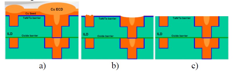
At the 2010 IEEE 3DIC in Munich Soitec presented more details on this process. Direct bonding, unlike thermo compression or eutectic bonding, is performed at room temperature under atmospheric pressure and is based on molecular adhesion between surfaces in contact. Cu-Cu direct bonding requires flat surfaces with surface micro roughness of both Cu and oxide materials of less than 1 nm for successful bonding. Soitec indicates that standard damascene copper CMP does not provide the desired surface topography needed for a successful bonding process due to Cu pad dishing and oxide erosion. An optimized CMP process has been developed to limit the surface topography between the copper pads and the surrounding oxide dielectric. The special CMP surface preparation step leads to very smooth surfaces, the micro-roughness of both Cu and dielectric surfaces beings as low as 4-5Å. In addition the CMP renders the surfaces highly hydrophilic with the contact angle below 5°. The figure below shows that the planarization steps a) and b) are common steps in damascene BEOL while the step c) represents a specific step required for Cu-Cu direct bonding.


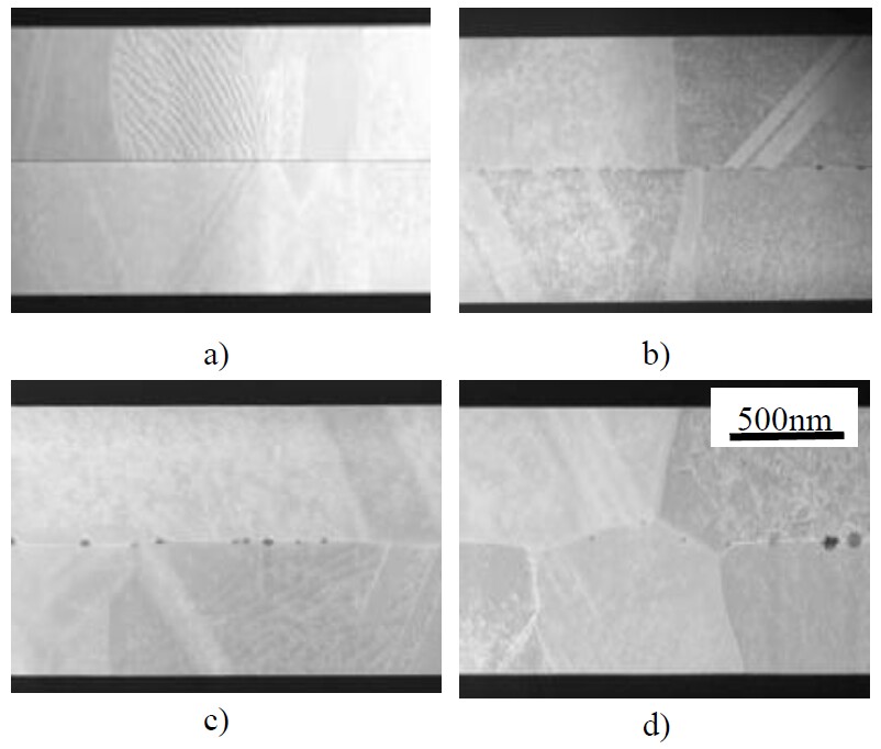
The figure below shows the cross section TEM images taken right after bonding (a)no annealing and after successive annealing steps at (b) 200°C, (c) 300°C and (d) 400°C during 30 minutes. Cu interdiffusion is apparent in the 200°C annealed samples, Cu grains being formed between the two layers. At higher temperatures, growth of copper grains is observed across the bonding interface.
In case of patterned Cu/oxide surfaces, oxide-oxide, Cu-Cu and Cu-oxide interfaces are formed during bonding. The bonding strength of the interfaces is shown in the figure below. The highest bonding energy is obtained for Cu-Cu interfaces, followed by SiO2-SiO2.
Bonding of 5μm Cu pads has been successfully performed with a corresponding bonding energy of more than 1J/m2 obtained upon 200°C post bond anneal. The bonding strength achieved has been sufficient to sustain post – processes such as silicon back thinning using coarse and fine grinding. Using a 5mm edge grind process, the backside thinning down to 5μm thin silicon substrate was realize with no delamination of the bond interface. Since no external force or pressure and temperature cycle is applied during bonding process, excellent alignment with minimum mechanical deformation is obtained.


Kansai Univ – “All Wet” Fabrication Technology


Some readers have pointed out that it has been several months since I gave a lesson on American idioms ( phrases which do not mean what the sum of the individual words mean). Certainly this Kansai Univ paper gives me the opportunity to do that.


As many of you know Alchimer has been reporting for several years on their “wet process” for insulation, barrier and seed [ see IFTLE 11, “In and Around the Moscone part 2”].


I have teased them in the past saying that I would indicate that their process was the only “all wet” process available. In general English usage in the US “all wet” means “completely wrong”. Searching for the original meaning of this idiom reveals it has been in use since the 1920’s although the origin of the meaning is unclear. I am sure the Kansai researchers are not meaning to describe their “fully wet” fabrication process as “completely wrong”.


The Kansai process uses electroless deposition of thin barrier layers of NiB and CoB catalyzed by the use of nano particles catalysts (Au, Pd, Pt) which are adsorbed on the SiO2 insulation of the TSV sidewalls that have been treated with 3-APS (3-aminopropyl-triethoxysilane coupling agent). A conformal electroless Cu layer can then be deposited on the barrier layer without catalyst by displacement plating.


Copper migration through the CoB and NiB barrier layers were examined by resistivity changes upon annealing. Cu / NiB was found to be stable up to 300 C and Cu / CoB up to 400 C.


Now, the community appears to have two options for a “fully wet” barrier and seed process.


ASET – 3D Architecture for Processor – Memory Integration


Ito of ASET described two 3D interconnection architectures (block and sandwich stacking) for stacked processor-memory LSIs. In the sandwich configuration, memory chips and processor chips are stacked alternately, and vertical interconnects in each PU-CHIP are divided into two groups: interconnects


for global communications and interconnects for local 3Dmemory communications. Compared with block stacking configuration, sandwich stacking architecture shows 38% fewer vertical interconnects for the same throughput and reduces power consumption by 21%.

The performances of three-dimensional stacking chips with 64- processor cores were also estimated. 3D in sandwich stacking architecture achieves twenty-times-lower power consumption of inter-chip communications than conventional 2D integration.


ASET – Copper / Polymer Hybrid Bonding


In another ASET presentation Aoki of ASET detailed their studies on copper / polymer hybrid bonding technology. We have seen copper / polymer bonding previously from both IMEC [ see PFTLE 10, “3D IC at the 2010 IEEE IITC” ].


For such bonding technology the surfaces of the metal and polymer must be globally flat. ASET applied a single damascene process for forming the hybrid bonding surface. To reduce surface-step height caused by copper dishing, a technology to co-planarize both the copper and polymer was developed. Polybenzoxazole (PBO) was used as the polymer for sealing bumps because it features positive-tone photosensitivity, high chemical resistance, and high thermal stability.


PBO polishing rate can be controlled by optimizing the PBO cure temperature. From the figure below you can see that curing the PBO at approx.. 280 C results in a very small step height ( less than 50 nm) which allows a globally planarized 200 mm wafer to be obtained.
For all the latest in 3D IC and advanced packaging stay linked to IFTLE, Insights From the Leading Edgeâ??¦â??¦â??¦


IFTLE 31 Oxide Bonding Patent Litigation Has Begun

As has been expressed on IFTLE many times, full 3D IC requires: TSV, thinning and bonding. As of yet there is no real clarity as to who “owns” any of these technology although there have been many boisterous claims out there being made.


In 2006 while the industry was deep in the R and D phase of 3D IC technology, I wrote a piece concerning “posturing and positioning” as the first phase of 3D IC technology commercialization [ “Posturing and Positioning in 3-D IC’s”, Semiconductor Int. April 2007]. The premise was that the 3D IC announcements at the time by Intel, IBM, Samsung, NEC, Elpida were the beginning of commercialization, stage (1) or “the bragging stage” if you will, where technology companies like peacocks strut around showing their feathers and announcing “we are the best”.


Stage (2) “real commercialization” came in 2010 when Elpida/UMC [see IFTLE 8, “3D Announcements and Rumors”]and Samsung [see IFTLE 27, “The Era of 3D IC Has Arrived with Samsung Commercial Announcement” ] announced 3D IC based memory products (albeit for late 2011- 2012). The expectation is that this will cause further announcements from competitor companies attempting to keep up in the technology race , a pattern we saw recently in the introduction of TSV technology for CMOS image sensors [see PFTLE 46,“…..on Mechanical Bulls, Rollercoasters and CIS with TSV” ].

Stage (3) I would define as the period where standardization begins to occur, the infrastructure begins to “gel” and technology ownership begins to clarify. For multilayered, complex technologies like 3D IC technology ownership is usually determined in the courts. Dec 6th 2010 is the date that initiated the technology ownership determination for “oxide bonding” technology. This is when Ziptronix filed a complaint against TSMC and Omnivision in Federal Court alleging “willful and deliberate” infringement of several patents [ USP’s: 7,387,944; 7,335,572; 7,553,744; 7,037,755; 6,864,585; 7,807,549; ] owned by Ziptronix pertaining to low temperature oxide bonding. The original SST article can be found here [link]. In question here is the use of oxide bonding for backside illumination in CMOS image sensors [see PFTLE 40, “Backside Illumination (BSI) Architecture next for Next Generation CMOS Image Sensors”]


Most of the CIS manufacturers have moved to BIS technology per a recent market study by Yole Developpment [ see “ CMOS Image Sensors Technologies and Markets -2010”].


Instead of illuminating a CMOS image sensor from the top side (front) of the die, backside illumination (BSI) collects photons from the backside so the light enters the device unobstructed by the metal and dielectric layers of the interconnect structure as shown in the figure.

According to Yole, CMOS BSI sensor technology is being used by Sony and has been announced in video camcorders and digital still camera products by Casio, Nikon, Ricoh, Samsung, JVC and Fujifilm.


Cell phone camera image sensor suppliers Omnivision, Aptina Imaging, Toshiba, Samsung and STMicro also appear ready for BSI products to appear in early 2011. Yole expects BSI technology to be responsible for a little over $1B (~17% of CIS sales) in 2012.


TSMC has presented their latest BSI technology in the paper "A Leading-Edge 0.9μm Pixel CMOS Image Sensor Technology with Backside Illumination:Future Challenges for Pixel Scaling" at the 2010 IEDM. They describe the "device wafer runs through a planarization process and is bonded with a carrier wafer. The bonded wafer is then mechanically and chemically thinned down from the bottom side of the device wafer to the target thickness". The process in question is the wafer bonding process. The qustion raised by this complaint centers around whether the accused are using oxide wafer bonding for their OmniBSI® technology, if so, whether the the oxide surfaces are treated with plasma or other chemicals and whether the Ziptronix claims in their numerous patents on the topic are indeed valid. TSMC and its subsidaries Xintec and VisEra appear ready to deliver CMOS image sensor devices to Omnivision.


Chipworks has done reverse engineering on Omnivision products such as the OmniVision OV5642 1.4 μm, back side illuminated (BSI) 5 Mp CIS [link] and teardowns of communication devices such as the HTC EVO 4G Smart Phone which they found contained the OmniVision OV8812 8 Mp Image Sensor chip (below).


BSI technology requires a solution for handling thinned wafers. A typical solution is to direct oxide bond the sensor wafer front surface to another oxide coated wafer which can then serve as a permanent “handle wafer” for the thinning operation.


Direct oxide bonding processes require extremely smooth (0.5 nm RMS) and clean surfaces which are readily achieved with standard CMP. When such SiO2 surfaces are placed into contact, they initially form relatively weak “van-der-Waals” bonds. Subsequent heating to elevated temperatures is necessary to achieve high bond strength through the formation of covalent Si-O-Si bonds. The high thermal budget required for this condensation reaction to proceed ( typically greater than 800 C) is not suitable for most devices, however, modifying the surface chemistry allows the formation of chemical bonds at significantly lower temperatures.


Recent reports from EVG indicate that oxide bonding currently has 35% better placement accuracy and better throughput than polymer bonding as shown in Table [ see PFTLE 41, “3D Integration Stays HOT at Semicon West”]


Using oxide bonding for the “back-end, bonding to carrier step” would result in low temp, high throughput bonding would result in excellent CTE match and positional accuracy.


Ziptronix technology for BSI is centered around ZiBondâ??¢ which they claim allows one to achieve significantly higher bond energy between wafers after treatment with various surface “activating and terminating” processes. The direct oxide bonding, which is initiated at low temperature, is characterized by a very high bond energy between the surfaces. One example of Zibondâ??¢ simply requires a plasma treatment followed by an aqueous ammonium hydroxide rinse. By such surface treatments bond energies in excess of 1 J/m2 are reported.


In 2008 Donabedian was quoted as saying that “the broad and fundamental nature of our patent portfolio, leads us to believe that any use of a oxide low temperature bonding process is highly likely to be covered by one or more of our patents” [“3D Startup Proves Ahead of Its Time”, Semiconductor International, Oct. 2008]. Donabedian further stated that “…while there are commercial tools in the market that claim to support low temperature oxide bonding processes, Ziptronix has not granted, nor does it intend to grant any licenses under it’s IP to the manufacturers of this equipment…anyone running a low temperature oxide bonding process as part of their manufacturing scheme is likely to be infringing on our IP” [“Ziptronix Pioneering 3D Integrated Circuit Process Technology”, i-Micronews, Aug. 2008]. Was this bravado or simply a statement of fact ? We will soon see !


Next week we will continue our look at presentations from the IEEE 3DIC in Munich.


For all the latest on 3D IC technology and advanced packaging stay linked to IFTLEâ??¦â??¦â??¦â??¦â??¦â??¦â??¦â??¦..


IFTLE 30 2010 IEEE 3DIC in Munich

In its new incarnation [see PFTLE 100, “3D IC in the City by the Bay” for historical perspective ] the IEEE 3DIC Conference met in Munich under the leadership of European co-chairs Peter Ramm (Fraunhofer EMFT Munich) and Eric Beyne (IMEC). Next years meeting (fall of 2011) will be held in Tokyo with Prof. Mitsumasa Koyanagi (Tohoku Univ) and Mr Morihiro Kada (ASET) as leaders. Below is a photo of this years session chairs and speakers “bookended” by chairman Peter Ramm on the left and old friend Fred Roozeboom on the right.
First we will take a look at cost modeling 3D processes and interposer technology and in hte next blog we will look at some other interesting presentations.

IMEC cost modeling


We would certainly all agree that the many reported manufacturing options for 3D integration could have a different impact on the cost of a 3D-stacked system. IMEC has developed a cost model to compare the costs of different process flows. The model revels a slightly lower processing cost for TSV middle (3D-SIC; 5 x 50 um) vs TSV backside (3D-WLP; 35 x 50 um); backside wafer preparation for Cu-Cu bonding and W2W Cu/Sn bonding as shown below.

Of great interest to IFTLE is the IMEC plot of processing cost (etch, liner, barrier, plate) vs TSV depth. Increasing the TSV depth at a given diameter (i.e increasing the AR while holding the diameter constant) affects etching, liner and barrier and plating negatively. In the chart shown below, one can see that SIC and WLP cross over at about 75 um. The model predicts a 40+% increase in cost to make a 5 x 100 3D-SIC TSV than a similar 5 x 50 TSV. Similar conclusions have been reached by EMC-3D [ see PFTLE 68 “Like Swallows Returning to San Juan Capistrano” ].


The model also concludes that the anticipated lower stacking yield of a W2W stacking strategy results in a higher cost for both the 3D-SIC and the 3D-WLP process flows.


Silicon Interposers


Papers from Fraunhofer IZM – EMFT Munich and RTI Int addressed fabrication aspects of 3D IC Interposers.


Weiland at IZM Munich described a 400 mm sq x 100 um thick interposer with 20 um dia TSV (5:1 AR) on 50 um pitch. The sidewall insulation consisted of thermal oxide followed by O3/TEOS SACVD (sub atmospheric CVD) and the barrier layer was TiW. The 3 layer RDL, built on the TSV is based on photo polymer (not identified) and plated copper. Wafer thinning to 100 um was done with a carrier wafer and temporary adhesive (stable to 150 Ë??C to allow backside deposition of low temp CVD SiO2.

Malta of RTI Int examined the fabrication of interposers by TSV first and TSV last processes. In the RTI backside TSV last process TSVs are formed after the front-side thin film processing is completed. It is not necessary to fill the TSVs since dry film resist can be used for patterning of back-side metal after the TSVs are formed. Since the vias do not need to be filled, TSV reliability concerns due to Cu-Si CTE mismatch are also reduced. One of the primary advantages of this approach is that the critical thin film processing is done on a blank Si wafer, with no limitations imposed by Cu-metallized TSVs. However, the TSV processes must be compatible with the thermal limitations of the front-side thin film layers which may include PECVD-TEOS or polymer dielectrics.


The biggest challenge occurs in making the interconnections between the TSVs and the front-side metal during “bottom clear” etch which selectively removes the insulator from the base of the TSV, exposing the metal, while not etching the sidewall isolation. Too much etching can result in high TSV leakage currents, due to sidewall passivation loss, while too little etching can result in high resistance interfaces.


In the TSV first process the TSV are etched as blind vias, from the front surface of the wafer. They are then passivated, coated with seed metal, and plated with Cu and the Cu overburden on the front-side is removed by CMP. The wafers are then thinned using backgrinding and back-side CMP, until the TSVs are exposed. After repassivation of the back-side, the interposers undergo front side thin film processing and backside metallization. A significant advantage is that the passivation “bottom clear” etch is not required, as in the TSV last approach. Also, since there are not other materials on the wafer at the time the TSV are insulated and filled, high temp processes such as thermal oxidation can be used to produce high quality oxide insulation. There is concern over the copper filled TSV CTE mismatch issues. Malta suggests that a way to address these reliability concerns is to “â??¦limit their diameter” but adds that “In order to have small diameter TSVs with an acceptable aspect ratio for processing, it may be ecessary to thin the wafer significantly. Most likely, freestanding wafers can only be thinned to a few hundred microns. Below that, the use of carrier wafers would be required not only for the thinning, but for any subsequent processing which remained” Current studies were done with 100 um dia TSV with 6:1 AR. TSV passivation was 2 um thermal oxide.


Back-side passivation tests was examined with photo BCB and PI. Malta did observe thermo mechanical issues during the curing processes at temperatures of 250ºC and 350ºC respectively. Distortion of the dielectric layers was observed in the areas over the Cu-filled TSVs, along with delamination and cracking of the films. RTI believes this is due to an protrusion of the Cu in the TSVs during the dielectric cure. Anneal tests at 400ºC for 1 hour in N2 indicated that the Cu in the TSV went through a permanent expansion of 1.5-2μm during the 400 C exposure as shown below.


For all the latest in 3D IC and advanced packaging stay linked to IFTLE, Insights From the Leading Edgeâ??¦.