Insights From Leading Edge

Yearly Archives: 2012

IFTLE 118 IMAPS 2012 part 2

Continuing our look at 3D and advanced packaging presentations at IMAPS 2012.

Shinko and CEA Leti

With the recent announcements by Xilinx, Altera and others the commercial production of 2.5D products on "high density" interposers is entering the realm of commercial reality. While it is clear that fine featured interpsoers will come from foundries like TSMC, there have been questions, about "coarse featured" interposers in terms of who will make them and what applications they will be used in. [see IFTLE 94, "Experts discuss interposer Infrastructure at IMAPS Device Pkging Conf"]

Shinko and Leti now describe integration and electrical characterization of such a "coarse featured" 3D silicon Interposer demonstrator for a SiP application. This demonstrator consists of (4) 10 Ã?? 10 mm chips mounted on a 26 Ã?? 26 mm Si interposer with 25µm microbumps on 50µm pitch and underfilled. TSV diameter are 10µm and interposer thickness is 100µm for an Aspect Ratio (AR) of 10. We are told that RDL on both sides of the interposer are done with a "semi additive process" although we are not given line width or pitch. We assume these are "coarse pitch" meaning 5µm or greater.

The populated interposer is then mounted on the PWB using Sn-57Bi solder to achieve low temp reflow. These packaged test structures were tested for TSV continuity and via chain resistance. These packages also survived 100 hrs at 125°C, 1000 cycles from -55 to 125°C, and 1000 hrs of HAST.

IBM Japan

IBM Japan reported on the warpage and mechanical stresses generated during chip and interposer assembly processes. Chip and package assumptions are shown below.

They modeled the following sequences:

Sequences are each divided into two steps, with either chip joining or interposer joining being the first step.

In the chips first sequence, interposer warpage is caused by CTE mismatch between interposer and RDL. Results are highly dependent on the thickness of the interposer. A 100µm to 200µm thick interposer can have more than 200µm displacement which will make it difficult to mount to the organic substrate. Underfill between the chips and interposer inhibits warpage.

Warpage of the interposer in the interposer to laminate first sequence is convex. A 100µm glass interposer shows less displacement than silicon.

The evaluated Von Mises stress on the interposer to substrate solder balls and found the largest stress was developed by the thickest silicon interposer and the lowest on the thinnest glass interposer.

IMEC

In their paper "Stacking Aspects in the View of Scaling", IMEC points out that when pitch goes below 40µm "stacking accuracy is one of the main drivers to ensure yielding devices." It is shown that stacking can be made less sensitive to in plane misalignment by the obvious options of increasing the pad size or decreasing the solder bump size, i.e. making the landing pads on the interposer larger than the bumps on the chip makes up for misalignment.

In a second presentation, "Small pitch microbumping and experimental investigation for underfilling 3D stacks," they report on 3D stacking characterization when using pre applied underfill.

For 3D stacking capillary underfilling has clear limits in terms of the gap between die and the bump pitch. This limits high density integration and therefore shifts focus onto pre applied underfill where the material is dispensed on the landing die before stacking. Pre-applied UF does have concerns such as transparency for alignment marks and UF/filler entrapment between bumps.

IMECs studies reveal that both NUF/NCP (define) and WUF (wafer underfill) have commercial products that result in >90% electrical yield after underfilling, although issues such as delamination of WUF films was observed.

Thin chip stacking using B2F technology

For many years PFTLE and IFTLE have been proponents of die thinning for 3D IC stacks because it not only has an effect on the final thickness of the product, but also has a direct effect on the TSV AR. When die are thinned to i.e. 25µm they can be stacked B2F without TSV and metallized over the edge to make interconnect. This technology was first described by Toepper from Fraunhoffer IZM.

In this presentation, ST Micro, CEA Leti, Datacon, Disco, and EVG presented two approaches have been investigated for B2F bonding of the thinned die: (1) applying a die attach film (DAF) bonding layer, or (2) using spin coated polymers for the die attach.

Thin die prep is required. In order to obtain good step coverage, die are singulated at 45° to provide edge slope. Once mounted on tape, plasma stress relief is applied. Without plasma treatment of the backside and edges, they found 100% of the die broke during the subsequent pick and place operation.

Using DAF is an acceptable solution but placement accuracy was degraded due to the presence of the DAF under the die and tool clogging by the DAF.

Spin-on polymer was found to be a better solution. They examined BCB, PI, and AL-X . PI showed outgassing and AL-X was not tacky enough so they down selected BCB.

For a capping insulation layer they examined: (1) conformal encapsulation by CVD low temp oxide; (2) thin conformal encapsulation by spin or spray coated polymeric films; and (3) thicker planarizing encapsulation using spin on polymers. The best solutions were found to be: (a) 200-240 C LTO in combination with the BCB adhesive layer, or (b) spray coating of positive, photo WPR 5100 from JSR. JSR thick resist THB151N was used to make contact from the top to the bottom chip.

For all the latest on 3DIC and advanced packaging stay linked to IFTLE………………..

IFTLE 117: Tezzaron acquires SVTC fab; 3DIC activity at IMAPS 2012 part 1

Tezzaron acquires Texas SVTC facility

Bob Patti of Tezzaron Semiconductor has been touting the merits of 3DIC for longer than most everyone else in our industry. Bob first announced a partnership with Chartered Semi to scale up his memory through-silicon via (TSV) technology back in 2007 [see PFTLE13: "50$ bonding and Intel announces ‘We are ready‘"].

Tezzaron has always been at the leading edge, offering 2µm pitch W TSV several years ago. Being ahead of the industry, frankly, they have had issues working through the regular supply chain.

Last week Tezzaron took a major step toward alleviating that problem with the announcement that it is acquiring the wafer fabrication facility of SVTC Technologies in Austin, Texas. You old-timers will recall this as the SEMATECH fab in Austin. Tezzaron will continue the operation of this facility while adding capabilities to assemble its own 3DIC devices. Tezzaron indicates that they will be operating the fab with the same employees in the same location.


IMAPS 2012

The 45th Symposium on Microelectronics (IMAPS 2012) was held a few weeks ago in San Diego. Let’s look at some of the 3D and advanced packaging papers presented at this meeting.

Qualcomm

When last we discussed Qualcomm it was complaining about constrained supply of 28nm [ see IFTLE 114, "…28nm; nickels and a symbiotic relationship"] but do we have any clarity on exactly what it is trying to build? Maybe now we do.

Gu and co-workers at Qualcomm reported on a memory on logic 3DIC stack consisting of a two-chip-wide IO memory stack bonded to a 28nm logic chip.

TSV are 6µm, wafers are thinned to 50µm, TSV connection is to M1 of the 7-layer copper/low-k interconnect stack. The memory stack has 1200 IO on 40µm pitch. The bottom memory die has TSV, the top die does not need them. Thinned die are shipped either on their carrier (OSAT removes the carrier) or after removal from the carrier on a flex frame.

Negligible shift in electrical parameters are observed after optimizing TSV formation and determining the need for a 5µm keep-out zone (KOZ). No change in bump resistance is seen after 1000 hrs at 150°C and 1000 cycles of temp cycling. Memory function was verified after full assembly of the stack.

Xilinx

Xilinx has been releasing information on its 2.5D FPGA module for the past two years. [See IFTLE 73, "Xilinx shows 2.5D Virtex 7 at IMAPS 2011" and IFTLE 23, "Xilinx 28nm multi-die FPGA, copper pillar advances at Amkor, and Intel looking at foundry options."]

In this latest presentation, Banijamail and co-workers examine the reliability of their 2.5D Virtex-7 H580T which consists of a transceiver chip and two FPGA slices. Interposer TSV are 10-20µm and 50-100µm deep. FPGA chips are bumped on 30-60µm pitch using Cu pillar bump technology.

Different substrate sizes and designs, lid designs, lid materials, and underfills were examined to minimize warpage and maximize microbump and c4 bump reliability. Control of these variables resulted in packages that met JEDEC warpage spec and minimized BGA fatigue.

Applied Materials

IFTLE has detailed many times how Applied Materials is making 3DIC a focus area for its equipment business. [see IFTLE 95, "Time flies when you’re having fun: Further details on the Micron HMC, equipment suppliers continue consolidation, EVG temp adhesive open platform" and PFTLE 72, "Samsung 3-D ‘roadmap’ that isn’t."]

Eaton and co-workers from Applied Materials now present process detail on how scallop-free TSV can be etched in their Silva etch chamber. Complete scallop removal added ~10-15% to the time to etch a 10 Ã?? 100 TSV with 30nm sidewall scallops.

SEMATECH

SEMATECH reported on their examination of the copper protrusion issue. While they quote a few past references such as my friends Paul Ho and Jay Im at UT Austin, to give credit where credit is due, they leave out what I think are the key references to the area [see "Researchers strive for copper TSV reliability," Semiconductor International, Dec. 3rd 2009], which include Bob Patti at Tezzaron whose cross-sections first brought the protrusion question to the public eye; Paul SibelrudPaul Sibelrud (then at Semitool) who extensively studied the extent of the problem and the composition of the extrusions; and most importantly Eric Beyne at IMEC who was the first to disclose the thermal anneal solution for the problem.

For those of you new to the area, after TSV are filled with copper and planarized by CMP they are subsequently exposed to >350°C downstream processing during which time Cu, due to a higher CTE, expands more that the surrounding silicon and extrudes out beyond the planarization point and stays there upon cooling due to its plastic deformation properties. This expansion also causes stresses to be generated which in turn require a KOZ (keep-out zone) to be defined so said stresses do not negatively impact the transistor electrical performance.

The goal of this SEMATECH study was to look for "possible mechanisms that cause copper protrusions by varying process conditions." The TSVs studied were 5 Ã?? 50 lined with 500nm of TEOS oxide and Ta/TaN diffusion barrier, which were then annealed at 150°C for an hour and CMP’ed. Samples post CMP were annealed at seven different temperatures .

The researchers outline a number of methods of detecting the protrusions and give +/- for them. They chose optical imaging and AFM as their methods of choice and micro raman spectroscopy to determine post-CMP anneal stress.

As expected, stress increases as the post anneal temp increases and copper protrusions range from 50nm to 400nm when annealed (post plating) from 150°C to 400°C. In agreement with the previous studies by Sibelrud, they find that plating bath chemistry has a major impact on protrusion. They link this to whether the copper is in a tensile or compressive state. They suggest that copper grown in a tensile stress state is a significant contribution to protrusions after thermal annealing at high temperature.

Next week we will finish our look at IMAPS 2012.

For all the latest in 3DIC and advanced packaging stay linked to IFTLE………………………….

IFTLE 116: A6 applications processor for iPhone 5 from Samsung, but…

Many of you may be wondering why IFTLE has recently been paying so much attention to the Apple A6 processor. Well, TechInsights reports that in the last 5 years Apple has generated over $150 billion in revenue from the iPhone family of handsets and accessories, and over 100 million units of the iPhone have been purchased by consumers [link].

We have mentioned before that the A6 is the odds-on favorite to be a major driver for bringing 3DIC (or at least 2.5DIC into high volume manufacturing). A few weeks ago we reported that TSMC felt confident about securing Apple’s foundry business for the A6 and A7 processors based on its 28nm and 22nm processes [see IFTLE 112, "TSMC staffing up for 2.5/3D expansion"]

Last week we informed you that the Taiwan Economic News had reported that pilot production of Apple processors was expected to start in the first half of 2013 with volume production following in the second half." [link]

Since the introduction of the iPhone in 2007, there have been five generations of iPhone models, each one improving on the technology used for the preceding model.

Comparison of Apple application processors [Chipworks]

Apple has partnered with Samsung for every generation of their application processors but recent Apple-Samsung lawsuits over patents related to competing handsets has lent credence to the rumors that Apple was going to switch production to TSMC.

What we now find is that this first generation of the A6 is still manufactured by Samsung as confirmed by both TechInsights [link] ("Our initial SEM cross-sections of the A6 processor show metal and dielectric layering that is almost identical to that used in the previous A5 processor … Early analysis of the die markings of the A6 reveal markings that are similar to the Samsung markings found in the A4 and A5 processors") and Chipworks [link] ("What we can say is that the foundry for the chip we have analyzed is confirmed to be Samsung and that […] this chip has a custom designed ARM core […] and has a triple core graphics processor unit").

Thus, multiple trusted sources agree that the A6 looks like it is being manufactured by Samsung 32nm technology.

The A6 is also the first Apple processor to use its own ARMv7 based processor design. The CPU cores aren’t based on the A9 or A15 design from ARM IP, but instead are something of Apple’s own design [link].

Apple A6 processor (Techinsights)

Conclusions

This information makes complete sense vs. the recent announcements indicating that TSMC was scaling up in 2013 (obviously not ready for last week’s production release). IFTLE concludes that it is likely that the 2nd-gen A6 will be done in 28nm technology by TSMC similar to the 45nm and 32nm versions of the A5 (as shown in the table above), and this is the point of entry for the TSMC 2.5D technology. The timing for this appears to be 2013. What Apple product will be the point of entry? IFTLE will stay on top of this evolving technology story.

For all the latest in 3DIC and advanced packaging, stay linked to IFTLE………………………

IFTLE 115: No nickels; SCP quals low-volume TSV manufacturing; 3D IC slowdown; Apple/TSMC timetable

Don’t believe everything you read!

Well, no sooner did we upload the blog last week [see IFTLE 114, "28nm capacity, nickels, and a symbiotic relationship"] than a local reader brought to my attention that the "Samsung pays off Apple in nickels" story was shown to be a hoax [link]. Even though my link was to Google-Nexus, not some crazy blogger with no credibility, I should have known better. I guess part of me simply wanted it to be true …. what a great move it would have been! Kind of like Clint Eastwood telling off the President of the United States. I asked the question, how and where do you get 20B in nickels? [Much less the logistical trouble of transporting 20B nickels weighing in excess of 100,000 tons.] So I should have followed my gut, or at least ran this by my BS meter! I guess I’m not any smarter than those who have spent the last 4 years "hoping for change" (pun intended) but never got it.

So I guess the only lesson we learned here is: Don’t believe everything you read.

STATS ChipPAC quals 300mm low-volume TSV manufacturing capability

STATS ChipPAC (SCP) has announced that its "TSV capabilities have achieved a new milestone with the qualification of its 300mm mid-end manufacturing operation and transition to low-volume manufacturing." [link] Reportedly SCP is engaged with multiple strategic customers on TSV development programs for the mobile, wireless connectivity, and networking market segments. Qualification activities include devices at the 28nm silicon node, application processors (AP), and graphic processors utilizing TSV for the high-performance wide-input/output (Wide I/O) memory interface required by higher-bandwidth applications for the mobile market.

The Company’s BEOL services include chip-to-chip and chip-to-wafer assembly with stealth dicing and fine pitch micro-bump bonding down to 40μm. Dr. BJ Han, executive vice president and chief technology officer, indicates that their "primary focus has been to develop high-volume TSV technology capabilities that we can offer to customers at cost points that make TSV a viable solution. We now have mid-end manufacturing capacity in place in Singapore and are actively engaged with multiple strategic customers on the production qualification of 2.5D and 3D packaging designs."

"3D IC commercialization to take place in 2015-16"

Someone I still do have faith in is ASE’s Ho Ming Tong, general manager and chief of R&D at ASE. According to Digitimes (Sept 6th 2012) he is being quoted as saying: "The adoption and commercialization of 3D TSV stacking IC technology and products will likely take place in the 2015-16 timeframe," whereas "2.5D TSV chips could be widely found in end products in 2014-15." [link]

Tong points to the fact that "electronic design automation (EDA) tools are not yet mature enough for the industry’s transition to 3D ICs from 2D ICs." When they finally do happen, Tong sees a broad array of applications including consumer electronics, mobile communications, PC, and automotive. The emergence of cloud computing is also expected to help accelerate the adoption of 2.5D and 3D TSV chips, he believes.

More on TSMC and Apple

In another story update, a few weeks ago we reported that TSMC felt confident about securing Apple’s foundry business for the A6 and A7 processors based on their 28nm and 22nm processes [see IFTLE 112, "TSMC staffing up for 2.5/3D expansion."] Well, the Taiwan Economic News now reports that "pilot production of Apple processors is expected to start in the first half of 2013 with volume production following in the second half." [link]

For all the latest on 3DIC and advanced packaging stay linked to IFTLE……………………

IFTLE 114: 28nm capacity nickels, and a "symbiotic relationship"

28nm yield reported to be up at TSMC

While Nvidia is the only customer to complain about poor 28nm yields at TSMC [link], other customers like Qualcomm and Altera have reported that "constrained supplies of 28nm" has affected their sales figures. Circulating rumors suggest that Qualcomm has looked for 28nm capacity at UMC and GF but has returned to TSMC since things were even worse at its competitors.

TSMC has announced a goal of getting its 28nm supply and demand into balance by the end of this year. According to the Taiwan Economic News, TSMC’s 28nm capacity is now running at 100,000 wafers a month, up from the 25,000 wafers a month capacity in Q2. TSMC’s fab 15 in the Central Taiwan Science Park is said to be ending Q3 with 69,000 28nm wafer per month capacity and will expand that to 135,000 wpm in Q4.

While there were widespread reports earlier in the year of severe 28nm yield issues at TSMC [link] according to Taiwan’s Commercial Times, equipment suppliers are reporting that TSMC’s 28nm yield is now over 80%.

But capacity shortage appears real and may constrain smartphone launches…….

There appears to be some concern that a shortage of available 28nm chip supply might constrain the new smartphone / mobile device launches this fall. Samsung and Sony lifted the wraps on new smartphones on Wednesday; Nokia, Motorola and Amazon.com are expected to do the same next week; and all leads up to the much-anticipated announcement of Apple’s iPhone 5, which many expect to happen on Sept. 12. [link]

At a recent investment conference, Qualcomm, maker of baseband chips and application processors (like Snapdragon) for smartphones and tablets, reported that it has had trouble meeting customer demand and is trying to ramp the supply as quickly as possible.

Would financial partners get better access to the available capacity?

Bloomberg reports that Apple and Qualcomm have made investment offers of more than $1B each, in order to set aside production capacity exclusively for them — but have been rebuffed by TSMC [link]. The report said that Apple’s proposal was aimed at securing an alternative supplier to Samsung for chips for its iPhones and iPads, while Qualcomm, leading supplier of application processors to the rival Android platform, needs to boost supply as shortages have impacted its earnings.

While TSMC refused to respond to what it called "market speculation," CFO Laura Ho did say that that "Dedicating one facility to a single product or customer creates the risk of a fabrication plant becoming a burden if the product, client or technology changes….You have to be careful. Once that product migrates, what are you going to do with that dedicated fab?"

The Bloomberg report says the smartphone chip market that is worth US$219.1 billion worldwide.

…And speaking of Apple and Samsung……

At present Apple relies on Samsung for its leading-edge A5 processor — but we all know about the high-profile legal dispute with Samsung over smartphones patents, and how Apple has been reported to be working with TSMC (Hsinchu, Taiwan) to bring up a 28nm A6 processor.

Apple may have won the recent Samsung suit concerning smartphones, but it appears that the joke was on them! [link] Google / Nexus reports that 30 trucks arrived at Apple’s headquarters in California to pay the required fine. Minutes later, Apple CEO Tim Cook received a call from Samsung indicating that over the next week they would be paying the $1 billion dollar fine in nickels. Do the math: this is 20 billion nickels.

Lee Kun-hee, Chairman of Samsung Electronics, told the media that his company is not going to be intimidated by a group of "geeks with style" and that if they want to play dirty, they [Samsung] also know how to do it. "They can use the coins to buy refreshments at the little [vending] machine for life, or melt the coins to make computers, that’s not my problem, I paid them and fulfilled the law."

IFTLE wants to know: (1) where Samsung was able to come up with 20B nickels ?? And (2) will Apple will use the nickels to pay for the next delivery of A5 chips??

ASE response to TSMC packaging expansion

A few weeks ago we discussed the fact that TSMC was recruiting engineers away from ASE and SIliconware to staff their 400 man packaging & test team raising questions about whether it might eventually challenge ASE and Siliconware in the packaging arena [ see IFTLE 112, "TSMC Staffing up for 2.5/3D Expansion…."]

The Taipei Times now reports that ASE is "brushing off concerns" of a potential rivalry with TSMC amid reports that the world’s largest foundry has put together a large team to make further inroads into ASE’s bread-and-butter market. They quote a senior ASE executive saying that "…the company hopes to have a symbiotic relationship with TSMC" in the future.

The traditional definition of symbiosis is "a mutually beneficial relationship involving close physical contact between two organisms that aren’t the same species," like birds eating insects of the back of a rhino.

In this case I think I know who the rhino is — and I think the rhino has decided to use bug spray and get the birds off his back!

For all the latest in 3DIC and advanced packaging stay linked to IFTLE…..

Recommended 2012 Coming Events:

IFTLE 114 …. 28 nm Capacity; Nickels and a “Symbiotic Relationship”

28nm yield reported to be up at TSMC

While Nvidia is the only customer to complain about poor 28nm yields at TSMC [link], other customers like Qualcomm and Altera have reported that "constrained supplies of 28nm" has affected their sales figures. Circulating rumors suggest that Qualcomm has looked for 28nm capacity at UMC and GF but has returned to TSMC since things were even worse at its competitors.

TSMC has announced a goal of getting its 28nm supply and demand into balance by the end of this year. According to the Taiwan Economic News, TSMC’s 28nm capacity is now running at 100,000 wafers a month, up from the 25,000 wafers a month capacity in Q2. TSMC’s fab 15 in the Central Taiwan Science Park is said to be ending Q3 with 69,000 28nm wafer per month capacity and will expand that to 135,000 wpm in Q4.

While there were widespread reports earlier in the year of severe 28nm yield issues at TSMC [link] according to Taiwan’s Commercial Times, equipment suppliers are reporting that TSMC’s 28nm yield is now over 80%.

But capacity shortage appears real and may constrain smartphone launches…….

There appears to be some concern that a shortage of available 28nm chip supply might constrain the new smartphone / mobile device launches this fall. Samsung and Sony lifted the wraps on new smartphones on Wednesday; Nokia, Motorola and Amazon.com are expected to do the same next week; and all leads up to the much-anticipated announcement of Apple’s iPhone 5, which many expect to happen on Sept. 12. [link]

At a recent investment conference, Qualcomm, maker of baseband chips and application processors (like Snapdragon) for smartphones and tablets, reported that it has had trouble meeting customer demand and is trying to ramp the supply as quickly as possible.

Would financial partners get better access to the available capacity?

Bloomberg reports that Apple and Qualcomm have made investment offers of more than $1B each, in order to set aside production capacity exclusively for them — but have been rebuffed by TSMC [link]. The report said that Apple’s proposal was aimed at securing an alternative supplier to Samsung for chips for its iPhones and iPads, while Qualcomm, leading supplier of application processors to the rival Android platform, needs to boost supply as shortages have impacted its earnings.

While TSMC refused to respond to what it called "market speculation," CFO Laura Ho did say that that "Dedicating one facility to a single product or customer creates the risk of a fabrication plant becoming a burden if the product, client or technology changes….You have to be careful. Once that product migrates, what are you going to do with that dedicated fab?"

The Bloomberg report says the smartphone chip market that is worth US$219.1 billion worldwide.

…And speaking of Apple and Samsung……

At present Apple relies on Samsung for its leading-edge A5 processor — but we all know about the high-profile legal dispute with Samsung over smartphones patents, and how Apple has been reported to be working with TSMC (Hsinchu, Taiwan) to bring up a 28nm A6 processor.

Apple may have won the recent Samsung suit concerning smartphones, but it appears that the joke was on them! [link] Google / Nexus reports that 30 trucks arrived at Apple’s headquarters in California to pay the required fine. Minutes later, Apple CEO Tim Cook received a call from Samsung indicating that over the next week they would be paying the $1 billion dollar fine in nickels. Do the math: this is 20 billion nickels.

Lee Kun-hee, Chairman of Samsung Electronics, told the media that his company is not going to be intimidated by a group of "geeks with style" and that if they want to play dirty, they [Samsung] also know how to do it. "They can use the coins to buy refreshments at the little [vending] machine for life, or melt the coins to make computers, that’s not my problem, I paid them and fulfilled the law."

IFTLE wants to know: (1) where Samsung was able to come up with 20B nickels ?? And (2) will Apple will use the nickels to pay for the next delivery of A5 chips??

ASE response to TSMC packaging expansion

A few weeks ago we discussed the fact that TSMC was recruiting engineers away from ASE and SIliconware to staff their 400 man packaging & test team raising questions about whether it might eventually challenge ASE and Siliconware in the packaging arena [ see IFTLE 112, "TSMC Staffing up for 2.5/3D Expansion…."]

The Taipei Times now reports that ASE is "brushing off concerns" of a potential rivalry with TSMC amid reports that the world’s largest foundry has put together a large team to make further inroads into ASE’s bread-and-butter market. They quote a senior ASE executive saying that "…the company hopes to have a symbiotic relationship with TSMC" in the future.

The traditional definition of symbiosis is "a mutually beneficial relationship involving close physical contact between two organisms that aren’t the same species," like birds eating insects of the back of a rhino.

In this case I think I know who the rhino is — and I think the rhino has decided to use bug spray and get the birds off his back!

For all the latest in 3DIC and advanced packaging stay linked to IFTLE…..

Recommended 2012 Coming Events:

IFTLE 113 An Exclusive Interview with Mr Lester Lightbulb

As readers of IFTLE might imagine, the recent headline "3M Claims new LED Lightbulb designed to burn for 25 years" caught my eye. The article went on to say that the bulb, which looks like a traditional incandescent, has a 25-year lifespan (at three hours of use per day) and a $25 price tag. 3M is betting the price won’t be a huge hurdle for consumers because competing LED bulbs "are priced closer to $45." They then repeated the infamous refrain: "LED light costs $1.63 per year to operate — a quarter of the cost of a traditional bulb. So even at $25, given its longevity, it still comes out where you save money over the life of the bulb."

The bulb uses 3M’s multilayer optical film, adhesives, and heat-management technology. They indicate that their marketing has determined that "prospective buyers are likely to be environmentally conscious and more affluent — similar to those who bought a Toyota Prius hybrid in 2006." IFTLE certainly agrees 100% with the last statement.

IFTLE has gone into great detail to show that it is the bulb that matters, not the expected life of the LED chip. If any of the components of the bulb are not rated for a 25-year lifetime the bulb should not be rated for this period of time. I checked the IFTLE BS meter for the merit of LED lightbulb ads and sure enough they rate just short of outright fraud.

As I shook my head in disbelief that this scam of the American public was continuing unabated, with no corrective information coming from the DOE or any other Government agency [yes that was said tongue in cheek], I got a collect call from old friend Lester Lightbulb. As you know Lester is sitting on death row in San Quentin [isn’t it fitting that California is the state that incarcerated him]. As he awaits the electric chair [pun intended] Lester reached out to admonish me for calling my recently failed CFL his "cousin" [see IFTLE 109: "2012 IEEE VLSI Conference ; Lester’s cousin CFLDies Prematurely"].

While I had him on the phone I thought you, the readers of IFTLE, would appreciate a direct interview with Lester.

IFTLE: Lester, of course we know that CFL and you are not related, we were just trying to link you, CFL and LED as part of the interior lighting family.

Lester: I’d like to thank IFTLE and its like-minded readers for supporting me as I await eradication from the face of the earth, but that dirtbag "quicksilver" is no family member of mine. Do you see a tungsten filament? NO. So he is certainly not related to me.

IFTLE: Quicksilver… is that his nickname?

Lester: Yes, that’s what all us incandescents call him — quicksilver is mercury and all the CFLs contain that highly toxic element. They are the least environmentally friendly source of light that we can use, which makes it quite ironic that those who claim they are trying to save the environment are about to eradicate me and use him. I guess you haven’t seen the latest headlines from Sweden have you?

IFTLE: No, please share them with us, Lester.

Lester: "CFLs creating ‘acute crisis’ in Sweden." In a series of articles the Swedish newspaper Svenska Dagbladet has reported on the large scale ongoing dumping of fluorescent bulbs (CFLs), and the dangers of released mercury that goes with it [link].

Mina Gillberg, former advisor to EU environment commisioner Margot Wallström is now regretting the consequences of their decision to switch to CFLs. "The motive for replacing incandescent bulbs with CFLs was to save electricity and thereby save the environment," but Gillberg now condemns the drive for CFLs as "absurd."

Sweden estimates that 200,000 CFLs are thrown into glass recycling bins per year. "‘This is a health risk for those who work with recycling and a risk that the environmental toxin spreads in the natural environment"…" Especially when the recycling bins are indoors, since mercury vaporizes at room temperature and contaminates the surrounding area."

IFTLE: So mercury or quicksilver is really that big a problem, Lester?

Lester: Mercury has long been recognized worldwide as a health hazard because its accumulation in the body can damage the nervous system, lungs, and kidneys, posing a particular threat to babies in the womb and young children. No one I have ever heard of, of any political persuasion, defends mercury.

The British government instructs households that "…if a compact fluorescent lightbulb is broken in the home, the room should be cleared for 15 minutes because of the danger of inhaling mercury vapour." Similar warnings are on US packaging where, as we have already discussed, the consumer is directed to contact the EPA for proper disposal procedures.

In 2009, timesonline [UK] reported extensively on the production of CFL in China, where "a heavy environmental price is being paid for the production of ‘green’ lightbulbs."

Tests on hundreds of Chinese employees found dangerously high levels of mercury in their bodies and many have required hospital treatment, according to local health officials in the cities of Foshan and Guangzhou. At the Nanhai Feiyang lighting factory in Foshan tests found 68 out of 72 workers were so badly poisoned they required hospitalization. In Jinzhou, 121 out of 123 employees had excessive mercury levels."

In 2008 Maine banned the disposal of CFL bulbs. In their tests CFLs were broken in a small/ moderate sized room and mercury concentrations in the room were continuously monitored. "Mercury concentration in the room air often exceeded the Maine Ambient Air Guideline of 300 ng/m3 for some period of time, with short excursions over 25,000 ng/m3, sometimes over 50,000 ng/m3, and possibly over 100,000 ng/m3 from the breakage of a single compact fluorescent lamp…. All types of flooring surfaces tested can retain mercury sources even when visibly clean….. Residual mercury in the carpeting has particular significance for children rolling around on a floor, babies crawling, or non mobile infants placed on the floor…. Vacuuming up the smaller debris particles in an un-vented room can elevate mercury concentrations over the MAAG in the room and it can linger at these levels for hours. And the vacuum can become contaminated by mercury such that it cannot be easily decontaminated." They indicated that the homeowner would have a decision on whether or not to "replace the carpet in the area where the bulb was broken."

Is anyone who is buying a previously owned home thinking about whether the carpet has been contaminated with mercury? And what that means to their small children?

So IFTLE, can you tell me why the world’s governments and the world’s self-described "environmentalists" are trying to eradicate the incandescant bulb and replace them with CFLs?

IFTLE: Lester, I think it’s all tied to the EPA. In 1990, EPA was given authority to control mercury and other hazardous air pollutants from major sources of emissions to the air. For fossil fuel-fired power plants, the amendments required EPA to conduct a study of hazardous air pollutant emissions. In 1999, EPA estimated that approximately 75 tons of mercury were found in the coal delivered to power plants each year and about two-thirds of this mercury was emitted to the air annually. In 2000, the EPA found that regulation of hazardous air pollutants, including mercury, from coal and oil-fired power plants was appropriate and necessary. Lester, don’t you think that this is a good thing? You can’t be for supporting mercury pouring into the atmosphere from our electric utilities, can you?

Lester: No, none of us are, but the electric utilities are taking steps to reduce mercury emissions from power plants as part of ongoing pollution prevention programs. In fact, existing control technologies for sulfur dioxide (SO2), nitrogen oxides (NOx), and particulate matter have reduced power plant mercury emissions by roughly 40 percent already. All of those nasty materials need to be scrubbed as does mercury, but notice I do not include CO2…and don’t get me started on that, because CO2 has gotten a worse bum rap than I have by the same ignorant environmentalists and corrupt scientists.

IFTLE: SOX, NOX and particuate reductions are all good things, Lester. I’m with you on the C02 emissions too, Lester. CO2 rates a 5+ on my BS meter, but we shall discuss that scientific fraud another day.

Lester: Anyway, my point is that instead of justifying toxic quicksilver light bulbs by pointing a finger at how toxic power generation is, why not continue to use safe, non-toxic, incandescent light bulbs and work on cleaning up the effluent from our power plants?

IFTLE: Once again you make sense, Lester. Let’s take a few minutes to discuss one of my pet peeves: CFL longevity. It’s claimed that a CFL will last ten times longer than an incandescent [It says so right on the packaging]. When my CFL bulb recently burned out faster than my incandescent bulbs [see IFTLE 109, "2012 IEEE VLSI Conference; Lester’s cousin CFL Dies Prematurely"], several readers reported that they too had experienced less than 1 year lifetime from their CFL bulbs. Hmmmm…

Lester: The basic problem is that quicksilver bulb lifetime is impacted by how often the bulbs are turned on and off and their use temperature. Optimal use for a fluorescent light is to be left on all the time at temperatures between 50-80°F. Wikipedia indicates that "In the case of a 5-minute on/off cycle the lifespan of a CFL can be reduced to close to that of incandescent light bulbs" — which is exactly the result that you got!

Since a lot of light use in the home is less than five minutes (i.e., a trip to the bathroom; looking in a closet; quick night time trip to the kitchen; get tool out of the garage, etc.), a much more accurate statement for CFL packaging would be: "Lifetime is estimated at 250-10,000 hours depending on use."

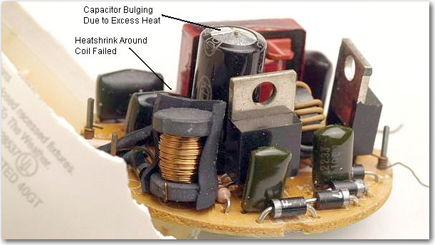
The picture below is of a CFL that failed after 200 hours [link]. The electrolytic capacitor is bulging at the end, and it had ruptured its safety seal and leaked electrolyte; the heatshrink tubing around the inductor got so hot that it split; and the capacitors are all seriously discolored.

The only way to get the maximum life from any CFL is to keep the electronics as cool as possible — preferably well under the manufacturers’ recommendation of 50°F.

Homeowners will also be faced with the expensive requirement to replace all non-ventilated light fittings with new ones that have sufficient airflow to maintain a safe temperature for CFL use. Because such fittings must be installed by a licensed electrician (in most countries), this is another expense that is usually ignored.

Any potential saving in energy bills is gone … for quite a few years, until the cost of the fittings and their installation is amortized. There is also the enormous waste of replacing perfectly good light fixtures with new ones, so the environmental impact is also negative — probably by a large margin.

By the way, IFTLE, I saw that you threw your CFL bulb away with the garbage. Hope you won’t be doing that anymore after our little discussion on mercury!

IFTLE: Wow, Lester, that’s a lot to think about. Anything else you want to share with our readers?

Lester: Yes, I’d like them to read the 2009 NY Times "green blog" interview with Howard Brandston. He is the award-winning lighting designer who helped develop the nation’s first standards for energy-efficient building design.

Mr. Brandston accuses "energy zealots" of using "faulty science" to determine the efficiency of light bulbs. To quote Mr Branston: "The calculations used by the government and others promulgating or promoting use of CFLs is strictly mathematical conjecture and has nothing to do with reality."

When asked whether we shouldn’t be doing all we can to cut down the amount of power usage, he responded: "But hoping that lighting is going to make a major contribution [to the reduction of power usage] borders on ridiculous. The real areas that should be looked at that would make big gains are in all commercial office buildings. If they raised the temperature in the summer that they would cool to and lowered the temperature that they would heat to […] we would save more energy in a few months than all the lighting watts per square foot baloney that’s going on now."

Basically, IFTLE, his conclusions are the same as yours when you looked at how much lighting contributed to the overall power usage in your house: "If you’re trying to save energy, that isn’t the place to start." [see IFTLE 98: Lester the Lightbulb vs. CFL and LED: The saga continues]

IFTLE: Lester, as always it has been a pleasure. I sincerely hope we can turn things around and get you a pardon, for your good and the good of the country.


For all the latest on 3DIC, advanced packaging and the exploits of Lester the Lightbulb stay linked to IFTLE…………………………

IFTLE 112 TSMC Staffing up for 2.5/3D Expansion ; Semi 3D Standards; Sony shows off 3D stacked Image Sensors

The Latest from TSMC

Ken Liu of Taiwan Economic News reports that TSMC is aggressively hiring for their 2.5/3D packaging and test unit and will have a team of over 400 specialists ready for this business area [link]. Reports are that they have hired experts away from ASE, Siliconware and Powertech to fill these vacancies.

In the past IFTLE  has insinuated that TSMC was working with a half dozen primary customers in the 2.5D area. Liu now names them as Xilinx, AMD, Nvidia, Qualcomm, TI, Marvell and Altera Corp.

Reports in Taiwan are that TSMC lost the chance for making Apple A3 processors to Samsung because of its lack of the capability to package and test the chips. TSMC management reportedly now feels confident of securing Apple’s foundry contracts for next-generation processors. The A6 ??
Per Steve Liebson here is a close up of the TSMC / Alterra  2.5D (which TSMC is now calling their chip-on-wafer-on-substrate CoWoS technology) test vehicle which we have previously described [ link]. It was evidently was on display at the Cadence booth at the recent design automation conference. TSMC describes the 2.5D circuit  as being composed of 65 nm GPS, 45 nm DRAM and 28 nm SoC.

(Click on any of the images below to enlarge them.)


3DIC SEMI Standards

The Inspection and Metrology Task Force  of  the Semi 3D standards group, recently approved its first Standard ,SEMI 3D1, Terminology for Through Silicon Via Geometrical Metrology. SEMI 3D1 will provide a starting point for standardization of geometrical metrology for selected dimensions of through silicon vias (TSVs). Although different technologies can measure various geometrical parameters of an individual TSV, or of an array of TSVs, such as pitch, top diameter, top area, depth, taper (or sidewall angle), bottom area, and bottom diameter, it is currently difficult to compare results from the various measurement technologies as parameters are often described by similar names, but actually represent different aspects of the TSV geometry.

Other standards under development by the  Inspection & Metrology Task Force include SEMI Draft Document 5270, Guide for Measuring Voids in Bonded Wafer Stacks, SEMI Draft Document 5409, Guide for Metrology for Measuring Thickness, Total Thickness Variation (TTV), Bow, Warp/Sori, and Flatness of Bonded Wafer Stacks, SEMI Draft Document 5410, Guide for Metrology Techniques to be used in Measurement of Geometrical Parameters of Through-Silicon Vias (TSVs) in 3DS-IC Structures, and SEMI Draft Document 5447, Terminology for Measured Geometrical Parameters of Through-Glass Vias (TGVs) in 3DS-IC Structures.

The Thin Wafer Handling Task Force is focused defining thin wafer handling requirements including physical interfaces used in 3D-IC manufacturing. Current standards for shipping are not well-suited for the reliable storage and transportation of thin wafers and dice on tape frames used in 3D-IC manufacturing. Wafer thicknesses of 30-200um will need significant changes to the current design criteria of current wafer transport and storage containers. SEMI Draft Document 5175 aims to address the robust handling and shipping of thin wafers, including changes in securing the wafers.

The Bonded Wafer Stacks Task Force is near completion of its SEMI Draft Document 5173, Guide for Describing Materials Properties and Test Methods for a 300 mm 3DS-IC Wafer Stack and SEMI Draft Document 5174, Specification for Identification and Marking for Bonded Wafer Stacks.

Current wafer standards do not adequately address the needs of wafers used in three-dimensional bonded wafer stacks for stacked integrated circuits. In each step of a 3D-IC process, the incoming material must be specified in terms of wafer dimension and materials present. Wafer thickness, edge bevel, notch, mass, bow/warp and diameters change when wafer stacks are bonded, debonded, and when wafers incorporated into stacks are thinned. Further, these parameters will change for a single wafer stack during process. This Document will provide the required properties of both silicon ("device") wafers and glass ("carrier") wafers to be used in 3D-IC applications. Templates for describing bonded wafer stacks and processed wafers to be used in the bonding flow would be provided as well.

The Middle-End Task Force is focused on the middle-end processes on wafers with or without TSVs, including post-final metal temporary bonding, wafer thinning, TSV formation and reveal, micro-bumping, redistributed line formation and carrier de-bond. The task force’s first two proposals are SEMI Draft Document 5473, Guide for Alignment Mark for 3DS-IC Process, and SEMI Draft Document 5474, Guide for CMP and Micro-bump Processes for Frontside TSV Integration.

Further details on the Semi standard efforts can be found here [link]. 

Sony Stacked Image Sensor

CMOS image sensors are used in a wide range of Sony products, including digital cameras, digital camcorders, DSLR cameras and Android based smartphones. Sony has focused on key traditional parameters such as increased pixel counts, improved resolution and higher speed. January 2012, Sony announced that it had successfully developed a 3D stacked CMOS image sensor complete with TSV. In place of the supporting substrate used in conventional back-illuminated CMOS image sensors, this image sensor stacks  the back-illuminated pixels layer onto chips containing the circuit section for signal processing which facilitates greater functionality and compactness. The new structure is positioned to become the next generation of back-illuminated CMOS image sensors.

 In the figure below Sony compares their new stacker CMOS image sensor to previous advancements such as Exmor (on chip column parallel A/D conversion) and Exmor R (backside illuminated). The size gains are obvious.
For all the latest in 3DIC and advanced packaging stay linked to IFTLE………………………

IFTLE 111 New Temporary Bonding Technologies Introduced at Suss 3D Workshop

At the recent Semicon West, Suss, which supports all commercially available temporary bonding solutions, held their annual 3D workshop.

(Click on any of the images below to enlarge them.)

IMEC
Eric Beyne of IMEC reported on 3D technology status. He sees:
– a clear industry convergence on Cu-TSV, vias middle with TSV dimensions 5 x 50 um. 
– a significant challenge is still a  wafer carrier system for wafer thinning with high precision and compatible with further backside processing
– as the technology matures they see a stronger emphasis on fine pitch die-to-die stacking : 40 µm Ã?? 20 µm Ã?? 10 µm
Beyne sees current application focus areas as:

When looking at all the studies performed on TSVs the literature offers the following conclusions:

IMEC is moving their standard process from 5 um in 50 um thick silicon to 3 um in 50 um thick silicon. They see this soon moving to 2 um TSV in 30 um silicon which is an AR of 15. They see the standard interposer as 10 um TSV in 100 um thick silicon.

Ga Tech

Venky Sundaram of GaTech updated the audience on "Glass as an Ideal Material for Interposers, Packages and System Integration." The two interposer programs at GATech are focused on Low Cost Silicon Interposers and Packages (LSIP); (a) wafer based; (b) panel based and Low Cost Glass Interposers; (a) wafer based and (b) panel based
According to Sundaram glass has the following attributes:


Although glass does have its challenges:

They see two commercialization paths for glass. They eventually see glass wafers as 2X less cost and panel based glass as 10X based glass. 

AMKOR
Ron Huemoeller of Amkor looked at the migration of SoC to 2.5D. This can occur by breaking up large pieces of logic into smaller chips and mating on an interposer or breaking up a large monolithic die into functions and mounting on an interposer.


The former is exemplified by the now infamous Xilinx FPGA interposer development which Amkor is in the process of assembly scaling up.

Amkor sees 2.5D assembly challenges as:

          Die-Die X-Y Spacing
       –      Fillet sizes and pad metallurgy and materials

        Process assembly sequence ; Micro-join method

          Die-Die / Die-Substrate Joining
       –        Micro bump uniformity ; Method of Join ; Materials
          Thermal and Power Management
       –        Use of Lids, Stiffeners and Passives
       –        Underfill/Resin bleed, adhesive compatibility
       –       Process assembly sequence and materials
          Warpage Control
      –        Interposer warpage ; Substrate warpage
      –        Top die warpage – area density/distribution
          Intermediate e-Test Points
      –        Process assembly sequence

Assembly options include chip on substrate, chip on wafer and chip on chip all of which have pros and cons.
This was followed by the introduction to tree new temporary bonding solutions that Suss is working on with Dow Corning, Dow Chemical and 3M.
Jim Rosson of Dow Corning introduced a bi-layer, temporary bonding solution with a  room temperature de-bond. This silicone solution consists of a WL-30XX Release layer and a  WL-40XX Adhesive layer.
De-bonding consists automated mechanical de-bonding at room temperature on Suss de-bonders
The wafer is solvent cleaned on flex frame with compatible solvents and the carrier wafer is cleaned by standard processes.
Dow Corning is currently expanding their beta test program of this temporary bonding system.
Jeff Calvert introduced Dow Chemicals new BCB based temporary bonding solution XP-BCB.
AP-3000 adhesion promoter is spun onto the carrier wafer followed by  XP-BCB onto active die wafer.
The temp adhesive is cured at 210-230C for 10-30 min. De bonding is done mechanically at RT due to the lower adhesion of BCB to the device wafer.
Blake Dronen of 3M described their next generation Wafer Support System (WSS).
Gen II WSS uses conventional WSS materials but adds a high temperature thermoplastic primer layer to the substrate surface as a surface for the UV curable adhesive to bond, independent of the wafer surface passivation material.  Upon laser degradation the LTHC layer and removal of the glass , the WSS adhesive joining layer can be peeled off the primer surface in a conventional manner.  The  thermoplastic primer is solvent rinsed, eliminating any opportunities for residue or imparting bump damage by the peel step.  This process reportedly will be ready for release in 4Q.
An LTHC free process is also being developed to simplify glass recycle and reduce overall process cost by eliminating the debonder laser. It uses the conventional WSS materials but replaces the LTHC layer with a 100% solids UV curable "release layer" that is tuned to enable mechanical separation of the carrier at the interface.   The adhesive joining layer, when cured, becomes a single component with the release layer, peeled as one during debond. The LTHC free process is currently being developed and optimized.

Chris Rosenthal of Suss reported on their  high throughput modular equipment platform for temporary bonding and debonding. Adhesive thickness requirements depend on the application:
Suss has concluded that room temperature lift-off debonding is fundamentally less risky than thermal slide debonding.
Suss introduced the XBC300 Gen2 for Room Temperature Debonding and Cleaning.

For all the latest on 3DIC and advanced packaging stay linked to IFTLE…………………………….


IFTLE 110 Samsung Breaks Wall of Silence at DAC 2012

Design Automation Conference  2012

At the design automation conference in June Samsung, who has been on absolute lockdown when it comes to 3DIC materials leaking out of the company, opened the door…just a little bit with Samsung foundry indicating that they will be  ready to release 3D TSV Technology and Wide IO Memory Solutions "in early 2013."

Samsung’s message as to the major attributes of 3DIC vs a package on package solution (PoP) are summarized in the slide below:

(Click on any of the images below to enlarge them.)

In terms of wide IO memory solutions they report that they will have wide IO DRAM (Non-JEDEC type ball interface) ready for customer sample in early 2013 and will also have JEDEC standard wide IO DRAM2 .

 They claim that TSV PDK and Design Methodology has been proven for  32nm node:

Not a lot of info, but at least an official indication that Samsung foundry is getting ready and we should be seeing products in les than a year.

Larger Silicon Interposers are Coming

Up to now, silicon interposers have been limited in x,y dimension to the field size of the steppers being used or 35 mm sq. It is no coincidence that the size of the Xilinx FPGA interposer is 35 mm.

At the recent Semicon West, USHIO (link) introduced a large-field stepper lithography tool targeting interposer fabrication for 2.5D/3D semiconductor packaging applications.

Using a 70 mm projection lens the new litho tool is capable of a  50 x 50 mm field size. They are also indicating that by 2013 they will be introducing  100 mm projection lens, which will increase the field size to 70 x 70mm.  Overlay accuracy is reportedly less than 500nm. Alignment is IR transmission based.

 EVG Wafer Bonding System first to Pass Equipment Maturity Assessment at Sematech
EVG announced that its GEMINI Automated Wafer Bonding System has become the first product to pass a systematic, rigorous Equipment Maturity Assessment (EMA) implemented within SEMATECH’s 3D Interconnect program. The Sematech assessments are designed to determine equipment readiness for high-volume manufacturing (HVM).

The  EVG GEMINI exceeded Level 3 equipment maturity requirements — the highest assessment rating awarded before transfer of new manufacturing processes into pilot lines or HVM.  Temporary adhesive bonding, silicon fusion bonding, and metal thermocompression bonding processes have been investigated on 300-mm wafer bonding system installed at CNSE in Albany, New York.

SEMATECH qualified wafer bonding alignment accuracy of less than 500 nm exceeding the wafer alignment specs of the ITRS for 2018.  Sitaram Arkalgud, director of SEMATECH’s 3D Interconnect program indicated that EVG is the first company to pass ISMI’s Equipment Maturity Assessment methodology.

 For all the latest in 3DIC and advanced packaging stay linked to IFTLE………………….