Insights From Leading Edge

Yearly Archives: 2012

IFTLE 100 IMAPS MINAPAD Addresses Advanced Packaging in Grenoble

"I’ve been a big fan of Phil’s ever since his first blog in August of 2007. Did you know he was born in Hell’s Kitchen in New York City? Congratulations to the world’s foremost expert on 3D integration on his 100th blog!" — Peter Singer, Editor-in-Chief, Solid State Technology

Dr. Phil Garrou has been blogging for years on the evolution of semiconductor assembly and packaging technologies. In his first 100 blog posts, he’s covered the emergence and explosion of 3D packaging, and most recently, the "2.5D" innovation of interposers.

To celebrate Dr. Garrou’s 100th post to Insights from the Leading Edge, we’ve compiled a list of his top 10 best-read recent blogs. You’ll find them at the end of this post………………

IMAPS France held the 2nd Micro/Nano-Electronics Packaging, Assembly, Design and Manufacturing Forum (MiNaPAD) in Grenoble in late April.

Jean-Marc Yannou, President of IMAPS France gave a Yole market update on 3DIC and TSV interconnects indicating that Wafer-level-packages are the fastest growing semiconductor packaging technology with more than 27% CAGR in units and 20% in wafers over the next 5 years to come.

(Click on any of the images below to enlarge them)

Yannou also repeated rumors that "Power 8 by IBM believed to be based on 3D interposers; Haswel, Intel GPU on 2.5D interposers for laptops with lots of on board memory and ultra large data bus. "
Leti gave an update on the 3DICE program being done under the European Unions 7th Framework with partners Datacon, Disco, EVG and ST Micro. Below find the unit operations that are part of the program and those responsible. They have concluded that B2F has less operations and is easier to accomplish than F2F.
Back to face attach can be done with die attach film, full sheet bonding layer or patterned bonding layer.
B2F pick and place with a Datacon 2200 can reportedly handle 20um thick die with 7um accuracy in 3 sec. Plasma stress relief allows for thin die handling by increasing die strength.
Thin die encapsulation can be accomplished in several ways i.e by conformal CVD deposition (oxide or parylene), by spin/spray coating of solutions (BCB, PI, ALX) or by film lamination. Die are bevel cut at 45 degrees to make subsequent metallization easier.
Thermo-mechanical stress in these combinations were examined.

EVG gave more details on the release process for their ZoneBond TB/DB (temp bond/debond) process.

– Adhesive ring dissolution is enhanced by magasonics                                                                                   
– Low force, room temperature separation                                                                                                        
– Compatible with both glass and Si carriers                                                                                                       
– Adhesives are (solvent)cleanable                                                                                                                    
– Platform enables use of a wide range of materials, i.e. ZoneBond Open Platform
The anti sticking layer showed a temperature stability up to 300C for 20 min. Carrier wafers were bonded and debonded 25x.
Rolf Aschenbrenner of the Fraunhoffer IZM made an in depth presentation on "Molding
technologies  – A new way for system integration" specifically looking at options for today’s transfer molding and compression molding technologies.

While transfer molding has been used for years to make plastic packaged parts, compression molding has recently become in vogue as part of the embedded chip technology package, i.e molded reconfigured wafers.

They propose the following roadmap for system integration with molding.

ST Micro presented some electromigration details on SnAgCu interconnect for WLB packages.
They find that:
 IMC induces resistance increase right after stress beginning
Electrical open is due to voiding in solder, at Cu3Sn interface, after Cu6Sn5 disappeared
Since the electrical opens are due to voids at the RDL/solder interface a solution is to insure that the enclosure around the solder ball is large enough and increase the RDL thickness as much as possible.  

We will have more MINAPAD review in next week’s IFTLE.
For all the latest in 3DIC and Advanced Packaging stay linked to IFTLE……………………..

10 Must-Read Insights from the Leading Edge:
1. Apple and TSVs, top chip makers, and "betting the ranch"

This post investigated Apple’s possible move to TSVs for its A6 chip, and compared capex numbers to the Western trope of "betting the ranch." Apple’s semiconductor roadmap, and the advanced packaging technology of TSVs combined for a compelling read. Link: http://electroiq.com/blogs/insights_from_leading_edge/2012/02/iftle-88-apple-tsv-interposer-rumors-betting-the-ranch-tsv-for-sony-ps-4-top-chip-fabricators-i.html

2. LED market is about to explode

While Insights from the Leading Edge covers a great deal of 3D packaging news, that doesn’t mean that there are no other very significant packaging evolutions and market opportunities going on at the same time. Certainly the LED space is one of those, Dr. Garrou said, and readers agreed.

Link: http://electroiq.com/blogs/insights_from_leading_edge/2011/11/iftle-75-led-market-is-about-to-explode.html

3. Bidding Adieu to Lester Lightbulb

Lester Lightbulb has become something of a favorite character on Insights from the Leading Edge, as Dr. Garrou carries out an in-home energy/cost savings analysis of conventional incandescent lightbulbs, CFLs, and LEDs.

Link: http://electroiq.com/blogs/insights_from_leading_edge/2011/08/iftle-63-bidding-adieu-to-lester-lightbulb.html

4. Advances in CMOS Image Sensing

In the fall of 2007, Toshiba first announced the commercialization of TSV in a CMOS image sensor (CIS). The next step of circuit repartitioning and stacking was interrupted by back side imaging, which flipped the chip over and let the light enter through the least obstructed side to let more light in per pixel. Now, we consider today’s CIS advances.

Link: http://electroiq.com/blogs/insights_from_leading_edge/2012/02/iftle-89-advances-in-cmos-image-sensing.html

5. Cell Phones and Memory Consolidation

The cellphone continues to pull in the functionality of digital cameras, PDAs, GPS navigators, mobile TV and numerous other applications. It is quickly becoming the dominant market driver for virtually all of these functions.

Link: http://electroiq.com/blogs/insights_from_leading_edge/2011/10/iftle-69-cell-phones-and-memory-consolidation.html

6. How Xilinx fit 6.8B transistors on its 2.5D FPGA

Garrou reviews Xilinx’s new FPGA, with 10,000 connections on a silicon interposer, using "2.5D packaging."

Link: http://electroiq.com/blogs/insights_from_leading_edge/2011/10/iftle-73-xilinx-shows-2-5d-virtex-7-at-imaps-2011.html

7. MEPTEC 2.5, 3D and beyond

Reporting from MEPTEC and SEMI’s "2.5D, 3D and Beyond Bringing 3D Integration to the Packaging Mainstream" Conference in 2011, Dr. Garrou shares highlights from Amkor, GLOBALFOUNDRIES, and other presenters.

Link: http://electroiq.com/blogs/insights_from_leading_edge/2011/11/iftle-77-meptec-2-5-3d-and-beyond.html

8. Fine Pitch Microjoints, Cu Pillar Bump-on-Lead, Xilinx Interposer Reliability

Dr. Garrou looks at packaging activities at the 2011 ECTC, including presentations from Qualcomm and STATS ChipPAC, Fraunhofer IZM, Xilinx (interposers!), and others.

Link: http://electroiq.com/blogs/insights_from_leading_edge/2011/07/iftle-58-fine-pitch-microjoints-cu-pillar-bump-on-lead-xilinx-interposer-reliability.html

9. TSV from 1999 to today, and more on the Micron HMC

Dr. Garrou shows us the evolution of TSV from 1999 through to today, checks in on MU’s HMC, and analyzes some recent packaging news.

Link: http://electroiq.com/blogs/insights_from_leading_edge/2012/04/iftle-95-3dic-time-flies-when-you-re-having-fun-further-details-on-the-micron-hmc-equipment-su.html

10. Defining 3D, and Canon’s packaging equipment foray

Garrou explains the variety of 3D packaging terms with a little help from "Raymond J. Johnson Jr." He also notes Canon’s back-end equipment entry.

Link: http://electroiq.com/blogs/insights_from_leading_edge/2011/08/iftle-62-3d-and-interposers-nomenclature-confusion-equipment-market-shift-to-pkging-continues.html

Here’s to 100 more Insights from the Leading Edge blog posts!

IFTLE 99 Electronic Design Process Symp (EDPS) focuses on 3DIC

A few weeks ago EDPS (the Electronic Design Process Symp) held a 3D day in Monterey CA. Riko Radojcic of Qualcomm gave a plenary on the “Roadmap for Design and EDA Infrastructure for 3D Products” and Arif Rahman, Altera, Steve Pateras, Mentor, Mac Greenberg and Bassillos Petrakis of Cadence followed in a session chaired by Herb Reiter of eda2asic, with  presentations on design and test challenges.

Qualcomm

Radojcic showed the following Xsect as what is becoming “mainstream technology” consistent with what the recent IMAPS DPC panel had to say [see IFTLE 94, “Experts Discuss Interposer Infrastucture at IMAPS Conference”] with 5 x 50 Cu TSV and solder capped copper pillar interconnect.

(Click on any of the images below to enlarge them)

It was good to hear Radojcic comment that “there are no intrinsic process technology show stoppers for memory on logic “ and that we just needed to get into volume production so we could exercise the processes.
For memory on logic he proposed the following as the status of the design environment:
Although Qualcomm has publically stated many times in the past that they ae not fans of interposers since they will increase the size of the devices while adding cost (amongst other things), Radojcic offered the following interposer challenges:
– low cost with fab like (1um pitch) routing may be hard
– timing driven routing may be had
– pre stack test may be hard
– managing Si with floating substrate may be hard

– fitting a small form factor at system level may be hard

Altera
Rahman’s talk for Altera centered on EDA needs for FPGAs. Altera had recently announced a program with TSMC to develop   heterogeneous 3D solutions that would combine an FPGA with a customer’s intellectual property, ranging from CPUs, ASICs,  ASSPs,  memory and optics.

TSMC is providing the end-to-end CoWoS (Chip-on-wafer-on-substrate — the internal TSMC name for their 2.5D process) process, including the front-end manufacturing of the die and the back-end assembly and test of the bare die on an interposer with TSVs connecting the bare die.
The Altera/TSMC team have developed a heterogeneous 3DIC test vehicle for this program.

Cadence


The theme for Bansal and Greenberg of Cadence was that “Wide-IO is driving 3DIC TSV”

We have discussed the easoning behind and the status of wide IO in the past [see IFTLE 87, “JEDEC wide IO standards…”] . Bansal shows a nice roadmap for future wide IO standards, and shows  
why wide IO will be needed in future products:
They conclude that Cadence stands ready with EDA tools and IP to enable your TSV designs with real experiences and partnerships with ~8 test chips and 1 production chip already completed.
We have discussed the Cadence [see IFTLE 72 “2011 IEEE 3 Test Wokshop”] and Mentor Gaphics DfT [see IFTLE 83, "Orange County 3DIC Workshop"] work on DfT previously. At EDPS both Bassilios (Cadence) and Pateras (Mentor) further discussed evolving BIST and other test flows for 3DIC.  I suggest you go to their respective web pages for complete detail on these important  test options.
Follow up on Lester the Lightbulb
These supportive messages were sent to me following last week’s blog:
"I started keeping receipts and writing down the dates on CFL bulbs I have purchased and so far have received three free replacements from the manufacturer as they tend to die in about a year [like incandescants] instead of 8000 hrs. This may in fact be the true savings to savvy consumers, as I may never have to buy another bulb again!!!"
“Thank you for being one of the ‘voices of reason’ in the LED debate.”
…………………….
For all the latest on 3DIC and advanced packaging stay linked to IFTLE………..

and proposed that the following gaps currently exist.

IFTLE 98 Lester the Lightbulb vs CFL and LED : the Saga Continues

In IFTLE 63 [ see IFTLE 63, “Bidding Adieu to Lester Lightbulb] back in Aug 2011 IFTLE attempted to make the case that our little 25 cent friend Lester the incandescent bulb had gotten a bump rap as he awaited extinction on death row.

It’s not that the claims of the newer technologies (CFL and LED) using less power than incandescent bulbs are invalid, but rather what appears to be the  bold faced lie that their much greater cost is  compensated by their decades long  lifetimes that upsets all Lester supporters.

My initial rant and my follow up comments [see IFTLE 82 “3DIC at the 2011…LED testing update”] tried to point out that the testing procedures were highly skewed to make things look like these new technologies were producing bulbs that would last forever. The main issue for me was that the other components found in teardowns of the LED bulbs certainly were not built to survive the LED lifetimes that were being claimed and the new bulbs will only last as long as their weakest component.

Our installed test LED and CFL bulbs  have now cleared 650 hrs of use. Only 24,000 more hrs to go to meet specs !

First a little update on pricing as of March 2012. The CFL are down to $4 each as shown below. They are still promising 9.1 years lifetime while using ¼ the power of an incandescent bulb. Oh yes, another minor issue is that when the do burn out it is recommended that you visit the EPA site to determine safe disposal…really that’s what it says !  

(Click on any of the images below to enlarge them.)

The Phillips LED bulb ( 75W equivalent since no 100 W equivalents are for sale yet) are selling for $40 at Home Depot with an incredible “expected lifetime “ of 22.8 years. Well at least you don’t have to contact EPA to determine how to dispose of them.

IFTLE has found several more articles indicating that our concerns were/are justified. For example Bill Schweber’s guest commentary in EE Times,  “CFLs and their issues" [1/10/2012] . “My concerns are with the lies that have been told to Congress and the public regarding lifetimes of the new technologies (CFL and especially LED), and the significant increase in toxic materials associated with the disposal of these short-lived cheaply made devices.”

"Although the lifetime of the LED devices may be rated at 40,000 to 100,000 hours at an appropriate temperature, just like we have all experienced with CFLs, the actual life of the device is generally much shorter due to higher temperature of operation of the device and due to the non-LED components in the assembly. After disassembly of several failed CFL devices and some LED devices, we as a community should understand that the cheap manufacture of such devices will lead to serious pushback and disillusionment of our customers.”

"The use of aluminum capacitors in CFL and LED Edison-base devices should be avoided at all costs, and yet it seems that every CFL and LED device I have disassembled, and the photos of every such device I have seen postings of disassembly for, use cheap aluminum capacitors with low temperature ratings. As consumers, most of us are aware that the CFL and LED Edison-base devices fail rapidly in closed fixtures, in outdoor use, in refrigerators and oven use…LED power output are specified at 25° and unless properly heatsinked, the higher the temperature the less light output with aging and less service life, probably 70° max temp is acceptable, but many work above this limit, so life span is not what is publicized.”

Giving credit where credit is due, IFTLE should note that the DOE takes a  good look at these issues in their second LED report “LED LUMINAIRE LIFETIME: Recommendations for Testing and Reporting” [June 2011].

Quoting from this report : The statement “100,000 hours of LED luminaire lifetime” is gradually giving way to the realization that there is little consistency, very little published data, and few hard facts around so-called luminaire lifetime numbers…sometimes only lumen depreciation…of the LEDs is considered in estimating useful life of the luminaire product…a problem, since failure or degradation of drivers, optics, or other components can lead to  total failure. Like other parts of the lighting system, the devices and components used to convert line power to direct current suitable to drive and control LEDs affect lifetime and reliability. Capacitors, inductors, transformers, opto-isolators, and other electrical components all have different design lifetimes, are affected by operating and ambient temperature, and are vulnerable to electrical operating parameter variations from surges, spikes, and so forth. An effective LED system-reliability evaluation must take all of these aspects into consideration… Additional information that should be readily available to the purchaser, although not on the label itself, should include maximum ambient temperature of operation to achieve this depreciation performance, the number of hours actually tested on which the projection is based, and the type of projection…”

These modifications to the initial DOE report were driven by articles such as  LED Driver Lifetime and Reliability hold thekey to success in LED Lighting Projects” by George Mao and Marshal Miles in the Sept/Oct 2010 issue of LED magazine.

Mao and Miles contend that “the light engine of properly designed LED lighting systems should last for up to 50,000 hrs. However, unless the power electronics…are designed for the correspondingly long life and high reliability, this will not be realized”   

Estimating the life of any product is primarily a matter of identifying all known wear out mechanisms and identifying the shortest lived component in the system that will render the product inoperable” Their choice for the component that would fail in the shortest time is the electrolytic capacitor. The temp that the fixture operates at appears to be a determining factor in the lifetime of such components.

Another concern is the hype surrounding how much money will be saved. IFTLE found this nifty little calculator on the Consumers Power web page. [link]  

What I have totaled up in the table below is pretty close to what power costs me in my NC home. Basically, for me , air conditioning is 75% of my power bill and even in the winter  Lester (incandescent bulbs) only account for 13 % of my power bill. 
Since this comes pretty close to my summer and winter electric bills, it shows that cutting my lighting bill by ¾ would save me ~ 36$ a year ( 3$ per month) which would pay for  less than 1 LED bulb per year and take me 25 years to break even on bulb replacement  in my house. It also confirms, for me, that in the average household, replacement of all the bulbs in the house with LEDs would not be seen on your monthly power bill. Sorry but the $3 savings will be lost in the noise.
On the country’s overall energy bill you may be able to see the effect, but on the average consumers monthly power bill, after spending $1000 to replace all the bulbs with LEDs, you will not ! The public is clearly being deceived !
Our friend Lester was set up, framed and is about to be executed for “the big energy lie” !
                                                  STOP the BS, SAVE LESTER the LIGHTBULB !
For all the latest in 3DIC and advanced packaging stay linked to IFTLE………..

IFTLE 97 DATE in Dresden, Synopsys 3D EDA Solution

This year’s Design, Automation and Test Europe Conference [DATE] was held in Dresden.  This year’s 1 day 3D Integration workshop was headed up by Sandeep K. Goel (TSMC), Qiang Xu (Univ Hong Kong) and  Saqib Khursheed (University of Southampton).

ARM, IMEC and the Swiss Federal Institute of Technology (EPFL) gave an interesting presentation on the "Performance and Efficiency of 3D Stacked DRAM in a Multicore System." The goal of this 2010 – 2012 European commission funded project, known as "Euro Cloud," is to integrate ARM processor cores with 3D DRAM for very dense, low power data centers for mobile cloud services for hand held devices. Coupling of high performance ARM Cortex processors with 3D memory is  targeting the mobile cloud services from Nokia which will serve millions of "mobile handsets."  Their analysis shows that although 3D-stacked DRAM, such as Wide-IO, allow for wider buses by providing increased pin density, the wider buses saturate in providing additional throughput. The authors propose that rather than increasing the width, more channels that are effectively managed by memory controllers lead to increased overall system performance. They also conclude that 2.5D is preferable to 3D for systems with challenging thermal performance.

(Click on any of the images below to enlarge them)

Hsien-Hsin Lee of Georgia Tech presented more details on their 3D MAPS massively parallel processor with stacked memory [we have discussed this previously in IFTLE 93, "2.5 / 3D at the 2012 IEEE ISSCC"] 
Of interest were their designs for V2 which will have 5 layers and a wide IO interface. It is shown schematically below with proposed specs compared to 3D MAPS 1
The Fraunhofer ASSID group presented their thoughts on quality inspection strategies for 3D chip processes. Their concept is that I line metrology is needed to save time and materials.
TSV metrology tasks include : determination of uniform TSV depth; barrier and seed defects and voids during TSV filling and  determination of bump height and coplanarity in copper pillar bump interconnect.
Synopsis unveils its 3DIC EDA solution
Synopsys recently  unveiled its comprehensive EDA solution, including enhanced versions of its IC implementation and circuit simulation products.
Synopsys reports that they are  delivering a comprehensive EDA solution including :

-DFTMAX: design-for-test for stacked die and TSV
-DesignWare STAR Memory System: integrated memory test, diagnostic and repair solution
-IC Compiler: place-and-route support, including TSV, microbump, silicon interposer redistribution layer (RDL) and signal routing, power mesh creation and interconnect checks
-StarRC Ultra: parasitic extraction support for TSV, microbump, interposer RDL and signal routing metal
-HSPICE and CustomSim circuit simulation: multi-die interconnect analysis
-PrimeRail: IR-drop and EM analysis
-IC Validator: DRC for microbumps and TSVs, LVS connectivity checking between stacked die
-Galaxy Custom Designer: specialized custom edits to silicon interposer RDL, signal routing and power mesh
-Sentaurus Interconnect: thermo-mechanical stress analysis to evaluate the impact of TSVs and microbumps used in multi-die stacks
The Synopsys 3D-IC solution is expected to be in production in calendar Q2 of 2012.
For all the latest in 3DIC and advanced packaging stay linked to IFTLE………………..

IFTLE 96 A New Concept for a 3DIC Conference; Granddaughter Update

In the past IFTLE has ranted about how every technical conference on the face of the planet wanting  a piece of the 3D integration pie and how that is propagating severe redundancy in the presentations that are being given.  Paying $500 + travel expenses for a conference that gives you 15 3D presentations when you have already seen 12 of them under slightly modified titles can be upsetting. Going to a conference that gives you 1 session of  3DIC presentations and you’ve seen all 5 of them is even worse.  I don’t blame the presenters,  because I know they are being begged by the session chairs to submit their presentations even if they admit that they have nothing new to say.

Having said that, I must admit I was intrigued by the concept of the new conference “Connect in 3D” being sponsored by Yole Developpement this coming  fall ( Oct 31st / Nov 1st). For those of you who haven’t seen the advertising blurb try this link [link]

The concept originated with Brian Perkins of Highliner Events (yes that would be Jeff Perkins brother – isn’t nepotism great).  While many conferences try to set up their schedule so that the attendees can have “quality networking time”  Brian’s concept is to  have a conference that is basically all networking complete with terms like “speed dating”.  Will it work for a technical area like ours ?

IFTLE decided to throw some questions Brian and Jeff’s way so we can all get a better understanding about how this works.

IFTLE: Brian How did this “connect” program come about ? Has it been used in other technical venues and if so how has it worked.

BP: The real value of a conference is no longer the presentations, keynote addresses, or even white-papers. It is the decision-makers and influencers who attend—and the networking and collaboration  that occurs between them at the event—that are truly high-value. Networking is the Holy Grail of event value, and our Collaboration SummitsSM are designed to deliver the maximum networking opportunities in a variety of pre-scheduled, formal and informal formats with a minimum of ‘pre-packaged’ content. Yole has used the technique for a MEMS event, I’ll let Jeff address how he felt that went.
 ï»¿ JP: We launched our first event with Highliner last year targeting the MEMS inertial sensor space. Attendees at  the inaugural “MEMS in Motion” event really embraced the format.  As a technical crowd, they “got it” very quickly, everyone used the software tools to the max and respected every meeting time limit – making the absolute most of their time.  Attendees gave us a 100% satisfaction rating. This event design is an iterative and evolving process. These second edition Collaboration Summits have been revised based on feedback and observations made during the first event. We will continue to respond to the market as it dictates.

IFTLE: Will attendance be capped by total or by company ?
JP: We would like to see no more than 200 participants. At sometime we might also consider capping the number of participants from a single company. The value proposition being more companies participating is better.
IFTLE: If I have read the material correctly it looks like two types of meeting are set up. Some by the attendee and some by a computer which matches up attendees randomly. Is that correct? How does this work?
BP:   The bulk of the meetings are scheduled by the attendees themselves.  Attendees request, accept and or decline meetings with other attendees.  These will be 20-minute meetings with delegates of their choice, scheduled through the DealCenter online platform or at kiosks during the event. Private tables are setup for conference attendees to meet with the person(s) they made appointments with through the DealCenter. Confirmed meetings will be assigned a table number in the Connect in 3D meeting area.  In addition, there is a session where there is “speed dating” pre-arranged meetings which we will talk about in a few minutesâ??¦.
JP: The DealCenter will open in September. Registered attendees will receive instructions in September via email when the DealCenter opens. All meeting planning is done through the DealCenter platform and every registered attendee will be able to see and request meetings with all other registered attendees. To be clear though – no contact information outside of the DealCenter contact point is ever made available unless users voluntarily provide it through their own meeting invitations or sent messages. So DealCenter is a temporary networking tool, setup for each event, allowing initial contact to be made, but any expansion of that contact is entirely up to you.
IFTLE: So all the attendees will be listed and I can privately sign up for 1 on 1 meeting with any of them before I get to the meeting. Those meetings are locked in – correct ?
BP: Remember the whole concept is about choice, so when I request a meeting with you, you have three options, you can accept the meeting, you can accept the meeting but suggest a different time, or you can decline the meeting. If you accept the meeting that is locked into our respective schedules.
IFTLE: What are the chances that the person I really want to meet will get booked up and I wont get to talk to him/her ? 
JP: It is entirely possible that the person you want to meet will be booked up for the 20-minute meetings, particularly if you wait until the last minute to register for the conference early bird registration really means something in this style event! However, all is not lost if they are booked – there is the possibility you will end up with a 10-minute speed dating meeting on the first day. Also there are all of the classic informal opportunities to meet: at the meals, we have extended coffee breaks and receptions. We actually enhance the ability to meet people by starting out the meeting with personal introductions. One of the key components to these events is the opening session introductions: so right after breakfast on the first day all of the participants gather in the plenary session room. We give a brief description of how the day will run, and then we begin the individual introductions.  It allows everyone to put a face with a name. If there is someone you really want to meet, you will know who they are and what they look like in the first 2 hours. You don’t have to wander around all day trying to read name badges.
 IFTLE: So how does the speed dating part work ?
BP: One of the important parts of any gathering of business professionals is the random connections that occur by serendipity. Our Meet the Market ( speed dating) meetings are designed to enhance that serendipity. These meetings will be set by the DealCenter program software a few days before the event. We want to be sure we have the maximum number of participants available to insure we capture everyone. The system will randomly pair attendees with other attendees screening for one meeting per individual from a given company and screening out anyone with whom you have already scheduled a 20-minute meeting.

IFTLE: What if speed dating assigns me to meet with a competitor, do I have to have those meetings ?

JP: The speed dating session is really about going with the flow.  We issue individual “date cards” minutes before the Meet the Market session starts and you go to each and every meeting, regardless of any sentiments you may have.  These meetings are 10 minutes – long enough to know if there is need to meet again, but not so long to make you uncomfortable.  At MEMS in Motion, even competitors that got paired up commented that they actually made a useful connection – serendipity indeed.   

 IFTLE: So what is the proportion of prepared materials (plenary presentations by experts / panel discussions) vs scheduled 20 min meetings vs speed dating over the two days ?

 BP : It breaks out to be just about 1/3 each  plus all the informal networking time at meals, breaks and receptions.  If you add in this informal time the breakdown is about 25% each
IFTLE : So to sum up, this is a conference which focuses on relationship building  through 2 days of networking in Palm Springs where you can get to have direct 1:1 meetings with people you have been wanting to meet ?
JP: In today’s world we are all too busy, the real point here is to make enough of a connection so that folks will pick up the phone when you call or open and reply to an email you send.
Update on the Girls
On the way to the IMAPS  Device Pkging Conf. stopped off in TX for the weekend to see how Hannah and Maddie  were doing. Ends up it was Rodeo weekend in Houston. Trust me you have never been to a rodeo till you’ve attended one in TX.  For those of you who do not understand why the Texas football team are known as the “longhorns” … Now you do !
For all the latest in 3DIC and advanced packaging stay linked to IFTLE………………..

Time Flies When Your Having Fun

Time Flies When Your Having Fun with 3DIC

Seems like yesterday that the packaging world was hearing that Fujitsu, Toshiba, NEC, Oki, Renesas and others had formed a pre-competative consortium under the Association of Super Advanced Electronics Technologies  to study direct connecting of chips with through silicon vias (TSV). It seems like yesterday but it was 1999, 13 years ago.  

In Feb 2005 my first article on the topic “Future IC’s Going Vertical” was published in Semiconductor International predicting that the industry would eventually have to move in this direction. A short month later, March 2005 I felt like a prophet when a TSV based 3D stacking approach was described by Intel’s Justin Rattner (todays CTO) at the Spring Developer Forum, with statements like “???????.. stacked wafers and stacked dies using thru-silicon vias are showing promise in meeting the memory bandwidth challenge.”

A year later, in April 2006 headlines from Soeul read “..  Samsung has developed a new "3D" package, which reduces space requirements and increases performance capabilities of today’s multi-chip packages. The company plans to use the technology to improve its NAND Flash packaging starting in 2007Samsung announced that its new wafer-level processed stack package (WSP) rather than using wire-bonding …. micron-sized holes that penetrate through the silicon vertically to connect circuits directly – TSV. According to Samsung the technology would enable manufacturers of mobile and consumer electronics devices to achieve better electrical performance and design slimmer and high-performance handset designs that provide improved battery time. The announced that the technology would enter mass production in 2007, for NAND Flash packages initially. And that they planned to use WSP for server DRAM stack packages sometime down the road.

A year later, in April of 2007, the headlines were “ IBM has announced that they’re relatively close to going commercial with a "through silicon via" (TSV) technology that will enable them to create high-bandwidth connections between two or more chips in a stacked packaging format." The big news about IBM’s design is that the company intends to start shipping product samples based on this technology in the second half of this year, with full production coming in 2008. "Looks as if TSV will be here faster than anyone previously thought."

Now, thirteen years later ASET is in its 3rd incarnation “the Dream Chip program” , it is obvious that DRAM will be stacked before NAND flash hopefully in HVM by 2013 (not 2007) , IBM has announced a major memory program with Micron (though not in 2008) and we are still awaiting any word of commercialization from Intel. Certainly it’s fair to say that this is taking a bit longer than we all thought, even those of us who were trying to be ultra conservative.

Micon / IBM  HMC – further details

IFTLE has been sent a few messages asking for further details on the Hybrid memory cube production.

Micron has announced that they will be manufacturing the memory layers and have contracted with IBM to manufacture the logic layer. Micron will be doing the assembly of the layers at a yet to be disclosed location. For now we can assume they are doing the initial production in Boise. For our initial discussions on this technology see IFTLE 74, “The Micron Memory Cube consortium”.

The technology described by M. G. Farooq of IBM last December at the IEEE IEDM [ see IFTLE 82 “3DIC at the 2011 IEDM???????”] is the technology being used to create the logic layer in the HMC stack (blue layer).

As noted in IFTLE 82, TSVs are integrated at “fatwire” (upper level metal) levels to optimize wire-ability and process complexity with 4 to 12 metal levels including low-k interlevel dielectric (ILD). TSV of < 100 µm depth were etched with near vertical sidewalls at a minimum pitch of 50 µm. An example of this is shown below. It is believed that the Micron logic layers  are being done in SOI technology.

The logic layer for the HMC parts will be manufactured at IBM’s advanced semiconductor fab in East Fishkill, N.Y., using the company’s 32nm, high-K metal gate process technology [link]
Chipworks has concluded that  “ it appears that the TSVs are annular. Once the lower metal/dielectric stack is formed (including the via dielectric for the metal layer that contacts the TSVs), the TSVs are drilled through to the silicon, and then a Bosch etch is used to drill the vias about 100 µm into the substrate, with a minimum pitch of 50 µm. After drilling, a conformal oxide is deposited, the barrier and seed layers are sputtered in, the copper fill is plated in, and any excess copper is CMP’d off. The dielectric for the contact level metal is put down, and then the top fat-wire metal levels are conventionally defined.” [link]
TEL acquires Nexx
Tokyo Electron Limited (TEL) has acquired semiconductor packaging equipment supplier NEXX.  Nexx advanced deposition equipment, including electrochemical deposition (ECD) and physical vapor deposition (PVD) tools will be added to the TEL line of products aimed at back end packaging applications and 3DIC.
Long time readers know that this has been a theme identified by IFTLE [ see PFTLE 41, “ 3D Integration Stays Hot at Semicon West” or PFTLE 107 "3D News:Applied/Semitool, TSMC, Ziptronix”

Looks a lot like the front end heavy weights Applied, LAM and TEL are going to buy up all the pieces they need to become the 3 heavyweights in packaging and 3D. Consolidation will continue because with fewer and fewer players moving to 22 nm and beyond packaging is a natural evolution for some of these big front end equipment vendors.
???

Shin-Etsu Joins EVG Temp Adhesives open platform
Shin-Etsu’s adhesives will be entering qualification trials on EVG’s EZR® (Edge Zone Release) and EZD® (Edge Zone Debond) modules, which support the new ZoneBOND??????? room temperature debonding process. Shin-Etsu is the first participant to announce for the program since its inception late last fall [ see IFTLE 76, “ Adv Pkging at IMAPS 2011: recent 3D Announcements”.
EVG’s ZoneBOND temporary bond / debond  solutions and open materials platform include:  the use of silicon, glass and other carriers; compatibility with existing, field-proven adhesive platforms; and the ability to debond at room temperature with virtually no vertical force being applied to the device wafer.  To support grinding and backside processing at high temperatures and to allow for low-force carrier separation, the concept defines two distinctive zones on the carrier wafer surface with strong adhesion in the perimeter (edge zone) and minimal adhesion in the center zone.  For further description of the technology see IFTLE 90 "Highlights from the IEEE 3DIC 2012 Japan" and refs therein.  

For all the latest on 3DIC and advanced packaging stay linked to IFTLE???????????????????????????????????..

IFTLE 95 3DIC – Time Flies When You’re Having Fun; Further Details on the Micron HMC , Equipment Suppliers Continue Consolidation, EVG Temp Adhesive Open Platform

Time Flies When You’re Having Fun with 3DIC

Seems like yesterday that the packaging world was hearing that Fujitsu, Toshiba, NEC, Oki, Renesas and others had formed a pre-competative consortium under the Association of Super Advanced Electronics Technologies  to study direct connecting of chips with through silicon vias (TSV). It seems like yesterday but it was 1999, 13 years ago.  

In Feb 2005 my first article on the topic “Future IC’s Going Vertical” was published in Semiconductor International predicting that the industry would eventually have to move in this direction. A short month later, March 2005 I felt like a prophet when a TSV based 3D stacking approach was described by Intel’s Justin Rattner (todays CTO) at the Spring Developer Forum, with statements like “…stacked wafers and stacked dies using thru-silicon vias are showing promise in meeting the memory bandwidth challenge.”

A year later, in April 2006 headlines from Soeul read “… Samsung has developed a new "3D" package, which reduces space requirements and increases performance capabilities of today’s multi-chip packages. The company plans to use the technology to improve its NAND Flash packaging starting in 2007Samsung announced that its new wafer-level processed stack package (WSP) rather than using wire-bonding …. micron-sized holes that penetrate through the silicon vertically to connect circuits directly – TSV. According to Samsung the technology would enable manufacturers of mobile and consumer electronics devices to achieve better electrical performance and design slimmer and high-performance handset designs that provide improved battery time. The announced that the technology would enter mass production in 2007, for NAND Flash packages initially. And that they planned to use WSP for server DRAM stack packages sometime down the road.

A year later, in April of 2007, the headlines were “ IBM has announced that they’re relatively close to going commercial with a "through silicon via" (TSV) technology that will enable them to create high-bandwidth connections between two or more chips in a stacked packaging format." The big news about IBM’s design is that the company intends to start shipping product samples based on this technology in the second half of this year, with full production coming in 2008. "Looks as if TSV will be here faster than anyone previously thought."

Now, thirteen years later ASET is in its 3rd incarnation “the Dream Chip program” , it is obvious that DRAM will be stacked before NAND flash hopefully in HVM by 2013 (not 2007) , IBM has announced a major memory program with Micron (though not in 2008) and we are still awaiting any word of commercialization from Intel. Certainly it’s fair to say that this is taking a bit longer than we all thought, even those of us who were trying to be ultra conservative.

Micon / IBM  HMC – further details

IFTLE has been sent a few messages asking for further details on the Hybrid memory cube production.

Micron has announced that they will be manufacturing the memory layers and have contracted with IBM to manufacture the logic layer. Micron will be doing the assembly of the layers at a yet to be disclosed location. For now we can assume they are doing the initial production in Boise. For our initial discussions on this technology see IFTLE 74, “The Micron Memory Cube consortium”.

The technology described by M. G. Farooq of IBM last December at the IEEE IEDM [ see IFTLE 82 “3DIC at the 2011 IEDM…”] is the technology being used to create the logic layer in the HMC stack (blue layer).

(Click on any of the pictures to enlarge them)

As noted in IFTLE 82, TSVs are integrated at “fatwire” (upper level metal) levels to optimize wire-ability and process complexity with 4 to 12 metal levels including low-k interlevel dielectric (ILD). TSV of less than 100 µm depth were etched with near vertical sidewalls at a minimum pitch of 50 µm. An example of this is shown below. It is believed that the Micron logic layers  are being done in SOI technology.
The logic layer for the HMC parts will be manufactured at IBM’s advanced semiconductor fab in East Fishkill, N.Y., using the company’s 32nm, high-K metal gate process technology [link]


Chipworks has concluded that “ it appears that the TSVs are annular. Once the lower metal / dielectric stack is formed (including the via dielectric for the metal layer that contacts the TSVs), the TSVs are drilled through to the silicon, and then a Bosch etch is used to drill the vias about 100 µm into the substrate, with a minimum pitch of 50 µm. After drilling, a conformal oxide is deposited, the barrier and seed layers are sputtered in, the copper fill is plated in, and any excess copper is CMP’d off. The dielectric for the contact level metal is put down, and then the top fat-wire metal levels are conventionally defined.” [link]

TEL acquires Nexx

Tokyo Electron Limited (TEL) has acquired semiconductor packaging equipment supplier NEXX. Nexx advanced deposition equipment, including electrochemical deposition (ECD) and physical vapor deposition (PVD) tools will be added to the TEL line of products aimed at back end packaging applications and 3DIC.


Long time readers know that this has been a theme identified by IFTLE [ see PFTLE 41, “ 3D Integration Stays Hot at Semicon West” or PFTLE 107 "3D News:Applied/Semitool, TSMC, Ziptronix”


Looks a lot like the front end heavy weights Applied, LAM and TEL are going to buy up all the pieces they need to become the 3 heavyweights in packaging and 3D. Consolidation will continue because with fewer and fewer players moving to 22 nm and beyond packaging is a natural evolution for some of these big front end equipment vendors.

Shin-Etsu Joins EVG Temp Adhesives open platform
Shin-Etsu’s adhesives will be entering qualification trials on EVG’s EZR (Edge Zone Release) and EZD (Edge Zone Debond) modules, which support the new ZoneBOND room temperature debonding process. Shin-Etsu is the first participant to announce for the program since its inception late last fall [ see IFTLE 76, “ Adv Pkging at IMAPS 2011: recent 3D Announcements”.
EVG’s ZoneBOND temporary bond / debond  solutions and open materials platform include:  the use of silicon, glass and other carriers; compatibility with existing, field-proven adhesive platforms; and the ability to debond at room temperature with virtually no vertical force being applied to the device wafer.  To support grinding and backside processing at high temperatures and to allow for low-force carrier separation, the concept defines two distinctive zones on the carrier wafer surface with strong adhesion in the perimeter (edge zone) and minimal adhesion in the center zone.  For further description of the technology see IFTLE 90 "Highlights from the IEEE 3DIC 2012 Japan" and refs therein.  
For all the latest on 3DIC and advanced packaging stay linked to IFTLE………………

IFTLE 95 3DIC â???????? Time Flies When You’re Having Fun; Further Details on the Micron HMC , Equipment Suppliers Continue Consolidation, EVG Temp Adhesive Open Platform

Time Flies When You’re Having Fun with 3DIC

Seems like yesterday that the packaging world was hearing that Fujitsu, Toshiba, NEC, Oki, Renesas and others had formed a pre-competative consortium under the Association of Super Advanced Electronics Technologies  to study direct connecting of chips with through silicon vias (TSV). It seems like yesterday but it was 1999, 13 years ago.  

In Feb 2005 my first article on the topic âÂ??Â??Future ICâÂ??Â??s Going VerticalâÂ??Â?? was published in Semiconductor International predicting that the industry would eventually have to move in this direction. A short month later, March 2005 I felt like a prophet when a TSV based 3D stacking approach was described by IntelâÂ??Â??s Justin Rattner (todays CTO) at the Spring Developer Forum, with statements like âÂ??Â??…stacked wafers and stacked dies using thru-silicon vias are showing promise in meeting the memory bandwidth challenge.âÂ??Â??

A year later, in April 2006 headlines from Soeul read âÂ??Â??… Samsung has developed a new "3D" package, which reduces space requirements and increases performance capabilities of today’s multi-chip packages. The company plans to use the technology to improve its NAND Flash packaging starting in 2007âÂ??Â?? Samsung announced that its new wafer-level processed stack package (WSP) rather than using wire-bonding …. micron-sized holes that penetrate through the silicon vertically to connect circuits directly – TSV. According to Samsung the technology would enable manufacturers of mobile and consumer electronics devices to achieve better electrical performance and design slimmer and high-performance handset designs that provide improved battery time. The announced that the technology would enter mass production in 2007, for NAND Flash packages initially. And that they planned to use WSP for server DRAM stack packages sometime down the road.

A year later, in April of 2007, the headlines were âÂ??Â?? IBM has announced that they’re relatively close to going commercial with a "through silicon via" (TSV) technology that will enable them to create high-bandwidth connections between two or more chips in a stacked packaging format." The big news about IBM’s design is that the company intends to start shipping product samples based on this technology in the second half of this year, with full production coming in 2008. "Looks as if TSV will be here faster than anyone previously thought."

Now, thirteen years later ASET is in its 3rd incarnation âÂ??Â??the Dream Chip programâÂ??Â?? , it is obvious that DRAM will be stacked before NAND flash hopefully in HVM by 2013 (not 2007) , IBM has announced a major memory program with Micron (though not in 2008) and we are still awaiting any word of commercialization from Intel. Certainly itâÂ??Â??s fair to say that this is taking a bit longer than we all thought, even those of us who were trying to be ultra conservative.

Micon / IBM  HMC âÂ??Â?? further details

IFTLE has been sent a few messages asking for further details on the Hybrid memory cube production.

Micron has announced that they will be manufacturing the memory layers and have contracted with IBM to manufacture the logic layer. Micron will be doing the assembly of the layers at a yet to be disclosed location. For now we can assume they are doing the initial production in Boise. For our initial discussions on this technology see IFTLE 74, ��?The Micron Memory Cube consortium��?.

The technology described by M. G. Farooq of IBM last December at the IEEE IEDM [ see IFTLE 82 âÂ??Â??3DIC at the 2011 IEDM…âÂ??Â??] is the technology being used to create the logic layer in the HMC stack (blue layer).

(Click on any of the pictures to enlarge them)

As noted in IFTLE 82, TSVs are integrated at âÂ??Â??fatwireâÂ??Â?? (upper level metal) levels to optimize wire-ability and process complexity with 4 to 12 metal levels including low-k interlevel dielectric (ILD). TSV of less than 100 µm depth were etched with near vertical sidewalls at a minimum pitch of 50 µm. An example of this is shown below. It is believed that the Micron logic layers  are being done in SOI technology.
The logic layer for the HMC parts will be manufactured at IBM’s advanced semiconductor fab in East Fishkill, N.Y., using the company’s 32nm, high-K metal gate process technology [link]


Chipworks has concluded that â�?�? it appears that the TSVs are annular. Once the lower metal / dielectric stack is formed (including the via dielectric for the metal layer that contacts the TSVs), the TSVs are drilled through to the silicon, and then a Bosch etch is used to drill the vias about 100 µm into the substrate, with a minimum pitch of 50 µm. After drilling, a conformal oxide is deposited, the barrier and seed layers are sputtered in, the copper fill is plated in, and any excess copper is CMPâ�?�?d off. The dielectric for the contact level metal is put down, and then the top fat-wire metal levels are conventionally defined.â�?�? [link]

TEL acquires Nexx

Tokyo Electron Limited (TEL) has acquired semiconductor packaging equipment supplier NEXX. Nexx advanced deposition equipment, including electrochemical deposition (ECD) and physical vapor deposition (PVD) tools will be added to the TEL line of products aimed at back end packaging applications and 3DIC.


Long time readers know that this has been a theme identified by IFTLE [ see PFTLE 41, ��? 3D Integration Stays Hot at Semicon West��? or PFTLE 107 "3D News:Applied/Semitool, TSMC, Ziptronix��?


Looks a lot like the front end heavy weights Applied, LAM and TEL are going to buy up all the pieces they need to become the 3 heavyweights in packaging and 3D. Consolidation will continue because with fewer and fewer players moving to 22 nm and beyond packaging is a natural evolution for some of these big front end equipment vendors.

Shin-Etsu Joins EVG Temp Adhesives open platform
Shin-EtsuâÂ??Â??s adhesives will be entering qualification trials on EVGâÂ??Â??s EZR (Edge Zone Release) and EZD (Edge Zone Debond) modules, which support the new ZoneBOND room temperature debonding process. Shin-Etsu is the first participant to announce for the program since its inception late last fall [ see IFTLE 76, âÂ??Â?? Adv Pkging at IMAPS 2011: recent 3D AnnouncementsâÂ??Â??.
EVGâÂ??Â??s ZoneBOND temporary bond / debond  solutions and open materials platform include:  the use of silicon, glass and other carriers; compatibility with existing, field-proven adhesive platforms; and the ability to debond at room temperature with virtually no vertical force being applied to the device wafer.  To support grinding and backside processing at high temperatures and to allow for low-force carrier separation, the concept defines two distinctive zones on the carrier wafer surface with strong adhesion in the perimeter (edge zone) and minimal adhesion in the center zone.  For further description of the technology see IFTLE 90 "Highlights from the IEEE 3DIC 2012 Japan" and refs therein.  
For all the latest on 3DIC and advanced packaging stay linked to IFTLE………………

Experts Discuss Interposer Infrastrucrure at IMAPS Conference

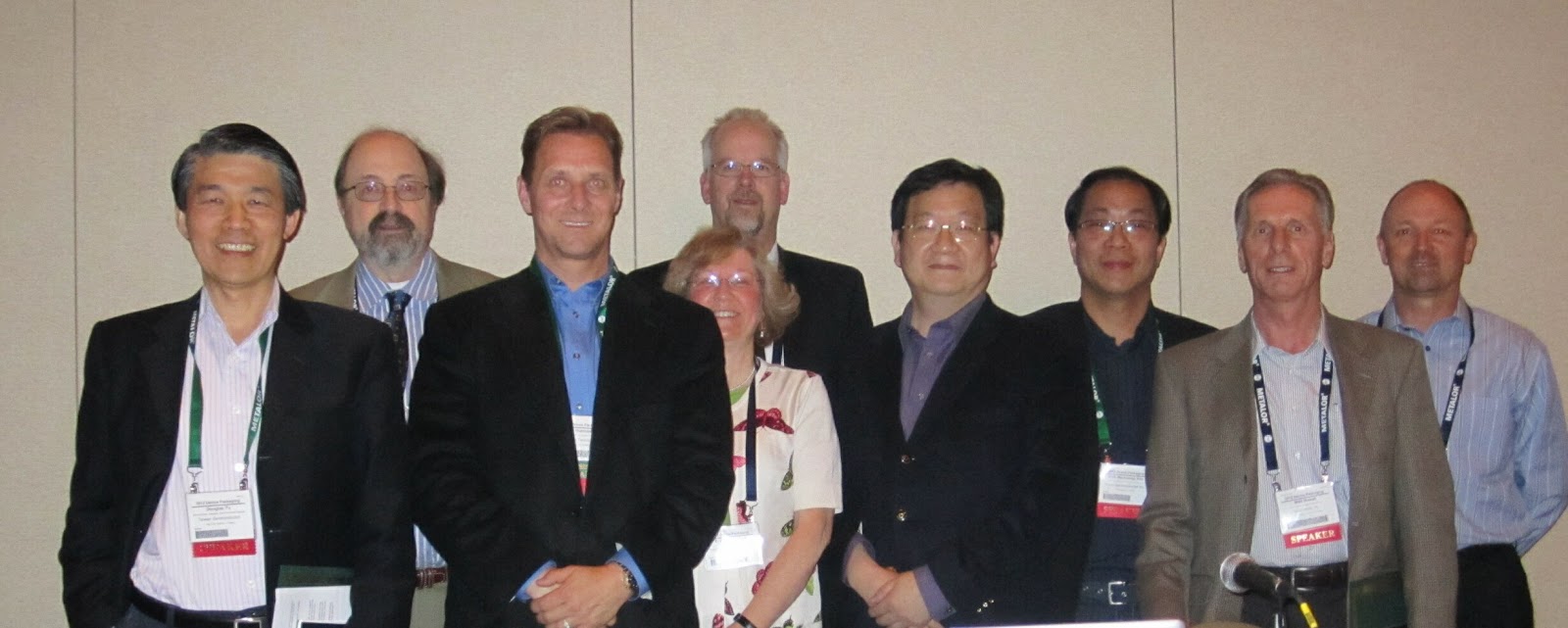
IFTLE brought together a  panel of manufacturers, users and market specialists at the 2012 IMAPS Device Packaging Conference in Fort McDowell AZ to discuss the Evolving 2.5D / 3D Infrastructure. [ Douglas Yu, Sr Director of front end and back end technology development for TSMC; Jonathon Greenwood, Director of Packaging R and D at GlobalFoundries;  Remi Yu, Deputy Division Director of UMC]memory suppliers [Nick Kim, VP of future electronic packaging technologies at Hynix] assembly houses [ Rich Rice, Sr VP of sales for ASE and Ron Huemoeller, VP of Advanced 3D interconnect at Amkor] users [Matt Nowak, Sr Director of Engineering at Qualcomm] and Market specialists [ Jan Vardaman, President of TechSearch Inc].

(Click on any of the images below to enlarge them)

       [l to r] Doug Yu [TSMC], Garrou [IFTLE],Huemoeller [Amkor], Vardaman [TechSearch],
Greenwood [GlobalFoundries], Yu [UMC], Kim [Hynix], Nowak [Qualcomm], Rice [ASE]
When asked whether 2.5/ 3D TSV technology has been narrowed down to copper TSV middle from IDM or foundries and some vias last backside all the panelists agreed with this conclusion. When asked about standard TSV dimensions, the foundry and OSAT representatives all agreed that 5-8 µm  on 50 µm thick Si looks like it has become the standardized offering that many of their customers are expressing interest in. When it came to interposers, they similarly all gave the nod to 100 µm thick interposers with ~ 10 um diameter TSV. 
Sourcing Interposers
A significant portion of the panels time was spent discussing current and future interposer sourcing. Assuming the attributes of “fine”vs “coarse” interposers as defined in the table below, the question becomes “where will these interposers be coming from” and “what will they be used for” ? 
So far announcements from Xilinx and Semtech indicate that they will both be using “fine pitch” interposers i.e fabricated by ~65 nm dual damascene [DD] CMOS processing by TSMC and IBM respectively. Altera and Nvida have also announced similar high density interposers for future use as have other graphics chip makers.
While all the OSATs have RDL technology capable of fabricating “coarse” interposers so far none of the major players [ ASE, Amkor, SCP, SPIL] have announced that they are entering the interposer business.
While all of the current roadmaps point to 2012-2014 as being the date for initiation of mass production for 2.5/3D products one must now ask where is the interposer production to meet this demand. If these lines are not in place now, is it easonable to think that products using them be qualified and in mass production within the next 24 months ?
During his conference presentation Amkors Huemoeller indicated that they would not be manufacturing interposers and their search of the industry for sources  indicated that only 3 players were close to being ready to deliver interposers that wee useful to Amkor, namely TSMC, UMC and GlobalFoundries.
 While glass panels and even possibly advanced laminates presented interesting possibilities for low cost future products, Amkor’s perspective is that  they are in the earliest stages of R&D.
All 3 of the foundry panelists indicated that they will be commercializing fine featured interposers although as we stated only TSMC and IBM had announced small volume product production has been initiated.
When asked about rumors circulating that OSATS are looking to put equipment in place to manufacture DD “fine pitch“ interposers, both Amkor and ASE indicated that they had no plans to do so.
IFTLE concludes that despite significant “industry chatter” the only programs that can afford interposers, so far, are programs that require the density or other attributes provided by fine featured interposers which can only be provided today by foundries /3D active IDMs. While we can anticipate that there might be products in the future that can be designed to take advantage of “coarse” interposers, and some of the initial fine interposer activities such as memory + logic + graphics chip applications might be able to migrate to coarse interposers as they become available, we will, initially at least, be limited by the availability and cost of foundry supplied interposers. 
The Evolving Infrastructure
TSMC reconfirmed  that they will provide full 2.5 / 3D service including chip design and fabrication, stacking and packaging [ see “2.5D announcements at the Global Interposer Techconferenceand “TSMC repeats call for foundry-centric 2.5/3D industry” ]
TSMCs Yu indicated that they have made their thoughts clear in the past few months and it can be found clearly delineated on their web page. During his plenary lecture Yu once again indicated that fabrication of chips on interposers was not as easy as making prototypes makes it look and they strongly favored controlling and being responsible for the full process.
When asked about supplying memory needs, Yu indicated that they would also handle that by having partnerships in place to supply the required memory although these partners were not identified.
When asked for their positions, UMC and Global Foundries indicated a preference to work under the open ecosystem model where chips from various vendors could be stacked and assembled by OSAT partners.
When asked how the current economic issues surrounding Elpida was affecting the UMC/Elpida/PTI partnership, UMCs Remi Yu responded that this was only one engagement that they had in place for 2.5/3D and that they were moving forward with others.
Amkor’s Huemoeller indicated that foundries would be supplying interposers and they [ the OSATS] would be assembling them.
 ASE agreed short term but indicated that longer term they envisioned a broad “pie” with space for several types of players. ASE envisions future applications where coarse interposers would find their niche and be an important part of the technology base
Both of the OSATS, as would be expected, favored the open ecosystem model where chips from various suppliers would be assembled at the OSATS. 
Qualcomm reiterated a position that they have expressed in the past which is that interposers would add substantial cost to 3D stacking and as such probably would not be a broadly accepted solution for low cost mobile products
TSMCs Yu responded that indeed the addition of an interposer added cost to  the overall component, but that “…this [2.5D] solution also offers cost savings by reuse of IP and separating digital and analog circuitry and allowing partitioning of costly SoC “ and that this in fact could make it the lowest cost solution..
When Hynix was asked whether they would be offering memory stacks containing TSV as have been already announced by Samsung, Micron and Elpida Hynix Kim responded that he expects “2 and 4 chip memory stacks with TSV to be in mass production in 2013”
When the panel was asked with the wide IO memory standard is now in place. what other standards were needed quickly Nowak of Qualcomm indicated that the upcoming Semi handling and transport standards were needed and noted that standardization was also needed in the ESD area and  standardization in the “design exchange formats” where he feels Si2 is taking the lead.
When asked for their opinion on the current status of design tools all 3 of the foundries indicated that current design tools are adequate to move forward. Qualcomm’s Nowak offered that logic on logic design tools were still lacking.
In terms of test strategies UMC would like to see some better standardization in the test area while Yu of TSMC drew a chuckle from the crowd when he noted that test needed to be minimized. Similarly, on the assembly front Rice indicated that ASE is having to test “everything” till the yields are up and Amkor quickly concurred.
Focusing on the first generation of 2.5/3D  stacking interconnect all accepted that this will be done with Cu/Sn eutectic by reflow or thermo-compression bonding.   When asked what was limiting direct Cu-Cu bonding all agreed that copper bonding was not ready for prime time just yet. Yu a strong proponent of copper interconnect, noted that current copper bonding options have yield issues that have not yet been overcome “current requirements for pads are too large and the required CMP of the interfaces is causing dishing that must be handled…HVM of copper –copper bonding options is tougher than showing research samples”
When similarly asked about  hybrid metal/oxide bonding schemes where oxide / copper surfaces are polished flat, oxide bonded then subsequently oven annealed to strengthen oxide bond and form Cu-Cu bonds (as shown by Ziptronix and Leti) no panel members were willing to say that this technology was close to commercialization.  TSMC responded that these technologies required very flat surfaces which were difficult to obtain due to dishing and other issues and that in general such technologies were “not ready right now”.  ASE expanded that this option was not required to solve todays problems and therefore was being looked at as a interesting R and D solution which could find its niche later. During Q and A Cook of Ziptronix offered that she thought their technology was ready and simply awaiting the commitment of a significant player. When the panel questioned copper migration issues due to miss alignment of the Cu-Cu bonds, Cook offered that their process which encapsulates the copper pillars in nitride barrier. 
Rumors abound that TSMC is designing the apple A6 processor for ipad and iphone with 3D TSV. When asked to comment on this or whether Samsung was also offering TSV in their design of the A6 this question brought the expected “no comment” from TSMCs Yu and silence from the rest of the panel. Similarly no one would offer up comment about who would be supplying Sony who announced that they would require TSV interposers for their next Playstation upgrade.
When asked about timing for the expected HVM of wide IO memory stacks for tablets, Qualcomm responded probably 2013 and Hynix responded maybe 2015.

For all the latest in 3DIC and advanced packaging stay linked to IFTLE…………….

IFTLE 93 2.5 / 3D at the 2012 IEEE ISSCC

There were several interesting 2.5 / 3D presentations at the recent IEEE ISSCC conference.

2.5D Integrated Voltage Regulator Using Magnetic Core Inductors on Silicon Interposer

Minimizing energy consumption is a performance goal of all of today’s devices including  microprocessors. Dynamic voltage and frequency scaling (DVFS) is a technique for performing “on-the-fly” energy-use optimization. Implementation of DVFS requires voltage regulators that can provide independent power supplies and can transition power supply levels on nanosecond timescales, which is not possible with modern board-level voltage regulator modules (VRMs).

Switched-inductor integrated voltage regulators (IVRs) can enable effective implementation of DVFS, but the primary obstacle facing development of IVRs is integration of power inductors. This work by Columbia University and IBM presents “an early prototype switched-inductor IVR using 2.5D chip stacking for inductor integration” by  combining magnetic materials, chip-stacking design and a 2.5D chip packaging process. The power converters integrated onto the same chip, or into the same package, as microprocessors "significantly improves computational performance per watt of power consumed

They report that the technology can reduce power consumption, by 10-20% in a typical US data center

Inductors are fabricated on the silicon interposer in an elongated spiral with a Ni-Fe magnetic core encasing the copper windings on the long axis.  “The Ni-Fe is deposited under a magnetic biasing field so that the hard axis of magnetization forms along the width of the core as shown in the figure. Inverse coupling between adjacent inductors, is utilized to avoid magnetic saturation of the core.” The inductor fabrication involves successive electroplating deposition of the bottom magnetic core, copper windings, and top magnetic core. The windings are electrically isolated from the bottom magnetic core with a layer of silicon nitride, and from the top core with ”hard baked photoresist”.

(Click on any of the images below to enlarge them.)

IBM Stacked Memory on Processor

There have been rumors out there that IBM would be applying with their 3D technology in their upcoming Power7 devices. Their presentation at ISSCC may be the first look that we are getting at their early designs for processors stacked with cache memory using TSV technology.

This work describes a prototype 3D system, constructed by stacking a eDRAM memory layer and logic blocks from the IBM Power7TM processor L3 cache, and a “processor proxy” layer in 45nm CMOS technology enhanced to include TSVs. The 3D stack is constructed using 50 µm pitch C4’s joining the front side of the thick processor chip to TSV connections on the back side of a thinned memory. The TSVs are Cu-filled vias that are ~20µm dia and <100 µm deep.

Standard design methodologies with some 3D extensions were used to design each stratum. TSV locations for power and clock were pre-defined to match a regular grid. Some sites were de-populated to accommodate the eDRAM blocks.

Tezzaron Technology Used for 2 Processors

Old friend Bob Patti at Tezzaron was involved helping fabricate two of the processor modules shown at this years ISSCC

Georgia Techs  3D-MAPS: 3D massively parallel processor with stacked memory

3D-MAPS (3D Massively Parallel Processor with Stacked Memory) is a two-tier 3D IC, where the logic die consists of 64 general-purpose processor cores running at 277MHz, and the memory die contains 256KB SRAM (see Fig. 10.6.1). Fabrication is done using 130nm GlobalFoundries device technology and Tezzaron TSV and bonding technology. Packaging is done by Amkor. This processor contains 33M transistors, 50K TSVs, and 50K face-to-face connections in 5 x 5mm2 footprint. The chip runs at 1.5V and consumes up to 4W, resulting in 16W/cm2 power density

Tezzaron 3D technology was used to stack two logic dies using face-to-face (F2F) bonding, where the top die is thinned to 12µm and the bottom die is 765µm thick.  These F2F pads are used for signal and P/G connections between the two dies. The diameter of a F2F bonding pad is 3.4µm, and their pitch is 5µm. 3D-MAPS uses 235 I/O cells that are placed along the periphery of the core die. Each I/O cell contains 204 redundant TSVs, where each TSV connects between a metal 1 landing pad and a backside metal landing pad deposited on the backside of the silicon substrate. Each backside metal landing pad (56 x 56µm2) is wire bonded to the packaging substrate. The diameter, height, and pitch of a TSV are 1.2µm, 6µm, and 5µm, respectively

University of Michigan Centip3De

David Fick of the University of Michigan showed Centip3De another processor fabbed by Tezzaron. A 3-D IC stack using 128 ARM Cortex M3 cores and 256 Mbytes of stacked DRAM operating at near threshold voltage. The module has an un-thinned cache layer and a thinned core layer with WB connecting to TSV on the backside.

Hynix Dealing with Process Variation in a 3D Memory Stack

In general, commercial DRAM shows large process variation from chip to chip, which causes address access time variation (tAC).  In order to reduce the tAC variation, most high speed SDRAMs adopt a delay-locked loop (DLL) at the cost of additional area and power consumption.   
Hynix in their paper entitled “A 283.2µW 800Mb/s/pin DLL-Based Data Self-Aligner for Through-Silicon Via (TSV) Interface explains that this can be an even larger problem for stacked memory die. “For TSV-based stacked dies, large tAC variation results in higher power consumption due to short circuit current from data conflicts among shared IOs”. Since the number of IO  might be 512 or more for wide IO DRAM,  the additional power consumption can be very high. While it is desirable in mobile DRAM to exclude the DLL because of the power cost , TSV stacked DRAM for high-speed operation partially adopts a DLL in the master die (driver circuitry) . The DLL-based data self-aligner (DBDA) described by Hynix  reportedly reduces the data conflict time among stacked dies, consuming 283.2µW during read operation at 800Mb/s/pin. It dissipates 4.98µW in self-refresh mode with the help of leakage-current-reduction controller.

For all the latest in 3DIC and advanced packaging stay linked to IFTLE…………..