Insights From Leading Edge

Yearly Archives: 2011

IFTLE 61 Suss 3D Workshop at Semicon West

This week, lets take a look at some of the presentations from the Suss MicroTech workshop “3D Integration – Are We There Yet” which was held at Semicon West in July.  

Eric Beyne,  IMEC Scientific Director for 3D Technologies, addressed the technical issues of carrier systems for 3D TSV thinning and backside processing. Beyne points out that right now silicon carriers are favored over glass because the glass, while transparent which allows for laser based optical debonding techniques, must be CTE matched to silicon over a large temperature range; ground to tight TTV specification (high cost ?) and has a negative effect on plasma based post grinding backside processes due to its low thermal conductivity.

After alignment and temporary bonding Beyne recommends the use of use of in-line metrology to allow for wafer rework if necessary.

Rama Puligadda, Mgr. for Adv. Materials R&D for Brewer Science gave an update on their ZonebondTM  room temperature debonding process.  The Zonebond process basically uses a 2.5 mm ring of adhesive to hold the wafer in place for grinding and backside processing which allows for easier subsequent debonding. The thin wafers are released from the carrier at room temperature after mounting on a film frame. Blanket UV exposure on the flex frame allows solvent removal of the temporary adhesive without damaging the adhesion to the flex frame tape.
Brewer has also developed a process with two carriers in order to achieve a wafer flip.

Stephen Pateras, Product Marketing Dir. at Mentor Graphics, gave a presentation on advanced design for test (DFT) and built in self test (BIST) for 3D-IC structures.  Pateras points out that TSVs can be used to create test access paths so that all BIST resources can be accessed on any device.
Pateras also concluded that all EDA players need to support common test access infrastructures since this will be required to stack die from difference sources. 
Eric Strid, CTO of  Csacade Microtech, indicated that they are using MEMS techniques to produce lithographically printed probe cards capable of 6 µm sq. x 20 µm high probe tips on 40 µm pitch which are being sold in research quantities.
Strid pointed out that standard pad locations will be required for vendor interchangeability and that standard materials specs for pads are needed in terms of materials, thickness and flatness. Such standard pad locations will enable standard test tooling.
Stefan Lutter , Bonder Project Mgr for Suss, discussed equipment and processes for temporary de-bonding. Suss reports that their open platform approach is capable of using any of the following bond/debond technologies. They see the industry trend as moving to the newer room temperature (RT)  release processes.

They claim that their HVM equipment, available 4Q 2011, will be capable of bonding and debonding 20-25 wafers/hr. The new Suss MicroTec product introduction is a HVM debonder/cleaner line for the RT release processes.
Thinned wafer on carrier mounted to flex frame are fed to these modules and thinned wafer on flex frame and detached carrier are generated. The technology uses a porous vacuum chuck to hold the thin device wafer that is mounted on tape and a flexible plate with vacuum grooves and debond initiator to peel-off the carrier. A schematic of the cleaning process is shown below.
For all the latest on 3D IC and advanced packaging stay linked to IFTLE


IFTLE 60 Semicon 2011: ASE, Alchimer, SPTS

Wu of ASE discusses Semiconductor Industry Status

At the recent Semicon West event in San Francisco, Tien Wu, COO of ASE, was the keynote speaker at the opening ceremony. Prior to joining ASE in 2000, Wu held several management positions within IBM.

According to Wu, the 53 years old semiconductor industry now accounts for 0.6 percent of worldwide GDP. He sees the semiconductor growth rate converging to ~ 7%. For the period 2011-2015 he is forecasting four years of stability with “mild growth” He sees this as a period of consolidation where only bold companies (“the bold ones”) will continue significant R&D and CAPEX spending. Wu described growth in the semiconductor industry over the past several decades as being driven by key applications. Aerospace in the 1970s, mainframe computers in the 1980s, PCs in the 1990s (global penetration now ~ 20%) cell phones in the 2000s (global penetration ~ 60%) and smart appliances in he 2010s . Wu noted that all of the applications are still running in huge volumes today.

Wu sees the industry polarizing into two factions ; (a) the infrastructure faction consisting of manufacturing heavyweights and (b) a systems faction [ IBM, HP, Apple] using software to interweave their product solutions and worrying about “branding “ their products. To quote Wu “The manufacturing heavyweights are driven by the systems power houses”

When comparing front end and back end operations Wu quoted figures showing that from 1980 to today $500B in CAPEX has been spent on the front end operations (avg of $26B/yr) whereas only $133B has been spent on the back end.

(ASE team joins COO Wu on stage after his Semicon Plenary lecture)

Alchimer Electrografting for MEMS, 3D and 2.5D Interposers
Steve Lerner, CEO of French startup Alchimer [see PFTLE 124; IFTLE 12] notes that progress is being made using their electro and chemi grafting products in the MEMS arena.  Earlier this year Alchimer  announced that the Microelectronics Innovation Collaborative Centre [C2MI (Quebec)]  had licensed Alchimer’s Wet Deposition process for MEMS 3D Research [link] to support the center’s 3D MEMS programs.
Luc Ouellet, VP of R&D at Teledyne DALSA Semiconductor (an earlier Alchimer licensee) reports that Alchimer’s electrografting technology “â??¦â??¦.provides strong support for work in advancing the technology for 3D MEMS manufacturing with a cost-effective approach”

Lerner also indicates that their new product family “AquiVantage” which provides metallization
for 3D Interposer and via last (backside) packaging is showing significant cost reduction for these applications.

AquiVantage uses the same basic technologies as the Alchimer’s wet processes for TSVs, reportedly providing concurrent wet deposition of TSV and front-side isolation, barrier, and copper fill/RDL, while eliminating CMP and dry deposition steps. It also supports smaller vias with higher aspect ratios. On the backside, the AquiVantage process allows selective maskless growth of the on-silicon isolation layer, eliminating an expose/develop/etch/clean lithography process cycle.

EVG


IFTLE sat down with Paul Linder, executive technology director and Markus Wimplinger director of EVGs business unit for technology development and intellectual property, to discuss their views on 3DIC commercialization and better understand their new temporary bonding metrology module which seeks to minimize the product at risk in a production environment.

Wimplinger noted that they have 1 customer already in production and that several are very close. Although they are wary to name names without customer approval , we have all seen their joint announcements with Amkor and their equipment installed at the joint programs of Leti / ST Micro and Fraunhofer Dresden and Global Foundries.

When asked to sum up their activity in the now retired EMC-3D consortium of which they were a co-founder, Linder indicated that the EMC-3D roadshows were helpful to show the industry that there is a supply chain for 3DIC and that the technology was doable. Linder reports that by the end, there was a clear consensus on a std process flow and all in all he views this as a very successful collaboration.

EVG has recently announced that they have joined the Ga Tech 3D Systems Packaging Research Center as a Manufacturing Infrastructure Member. Linder indicates that their mission is to develop “â??¦technologies that will make silicon and glass interposers with TSVs a truly affordable packaging solution." EVG’s temporary bonding and debonding, chip-to-wafer bonding and lithography technology and process know-how will be included in the PRC’s Silicon and Glass Interposer Industry Consortium research program.

EVGs new inline metrology module reportedly allows customers to implement in line process control for thin wafer processing. The in line metrology module can detect a variety of process irregularities and defects during temporary bonding and debonding including the TTV (total thickness variation) of the carrier wafer, adhesive layer, bond stack and thinned wafer; bow/warp of the boded stack and voids in the bond interface.

For all the latest in 3D IC and advanced packagign stay linked to IFTLE…………………

IFTLE 59 Thin Film Polymer Apps from the 2011 ECTC; Tezzaron 3D Activity

Polymer filling technology for Vias last (backside) TSV

Leti presented informative data on polymer filing of vias last (backside) TSV. The normal Leti process a wafer is bonded on a temporary glass carrier and thinned down to 120µm. 40-60µm diameter vias are then performed by DRIE in silicon. A 2µm thick SiON insulation layer is performed by PECVD. A plasma etching is then performed to open contacts on metal level in TSV bottom. Due to the TSV dimensions complete filling with a metal is not appropriate due to issues including process time, process cost, metal overburden thickness and thermo-mechanical stress. For these reasons, a copper liner is electroplated inside the TSV. This liner also forms the RDL layer on the wafer bottom surface. A 7µm thick polymer layer is then coated on the RDL in order to insulate it This layer, realized by spin-on of a liquid polymer, tents the RDL and TSV without filling it, as shown in the figure below. This leaves the copper liner inside the TSV exposed to trapped air (oxidation).  In addition, the thin polymer layer over the TSV is a weak point where temperature variation (during following process steps or device lifetime), can break or crack the layer.

In the modified "polymer fill" process a 20 to 30µm thick polymer layer is coated by spin-on on the wafer. Vacuum heating is performed decreasing the polymer viscosity and  allowing easier removal of the air trapped in the TSV. Temperature and the pressure during the vacuum heating has to be optimized for each different polymer in order to obtain complete filling of the TSV.

Trials have been done with two polymers having different thermomechanical properties (see table ).

Polymer 1 has a higher Young modulus and a lower coefficient of thermal expansion than polymer 2. Results show that polymer 1 induces more warpage in the thinned wafer than polymer 2
Fan Out WLP by RDL first Method
Researchers at Renesas described a unique process flow for achieving fan out WLP (FOWLP) by an RDL first method.  The fabrication technology used for most FOWLPs is a chips first method (shown in the figure below) where the chips are mounted to a carrier face down; the chips are molded into a wafer and the carrier removed; RDL and terminations are formed and the packaged chips subsequently singulated.  Renesas repots limitations to this process flow include (1) The I/O pitch of the embedded chip is limited by alignment mismatching between the chip and the RDL; and (2) The RDL requires a low-cure temperature resin which may negatively affect package reliability.
Renesas suggests a RDL first approach which they note is based on their earlier work with NEC on the SMAFTI program ( smart chip connection with feed through interposer). The process flows are compared below.

They claim that a finer chip I/O pad-pitch is achieved due to better CTE  matching between the die and support wafer and that the high-cure-temperature resins used, make the RDLs more reliable. Their name for this is SiWLP for SiP (system in package) WLP. Another acronym I greatly dislike since it will always be interpreted as "silicon WLP" for obvious reasons.

The figure below compares a WB-BGA solution to a SiWLP solution for a 6 mm2 analog chip and a 3 mm2 microcontroller. It indicates that the SiWLP enables a 57 % reduction in area compared to conventional WB-BGA-type SiP.
Mechanical Properties of Thin Film Polymers
A joint publication between RTI Int, U Texas-Austin and Microelectronic Consultants of NC took a close look at the mechanical properties of low temp ( ca 200 C) cure polymers [Asahi Glass-ALX; Hitachi-DuPont-PBO and JSR-WPR 5200]used in RDL type applications. Getting thin film specimens [10-20µm thick samples] properly fabricated and loaded into a test system is not a trivial task. Reproducible data requires samples that are lithiographically prepared (not cut with a razor blade) and requires compliance correction factors be calculated. The following table shows vendors reported data vs data gathered in this study. Manufacturer reported modulus numbers were in all cases off significantly (ca 50%) and in some cases elongation and tensile strength numbers showed quite a large spread indicating that even in this study, where extreme caution was taken to prepare the samples, flaws must have been present.
Tezzaron
PFTLE and IFTLE have previously covered Tezzaron, one of the pioneers in 3D IC [ see PFTLE 125, PFTLE 115, PFTLE 90; IFTLE 8, IFTLE 28]
We recently revealed that MOSIS working with Tezzaron and Mentor Graphics would now allow users to test out 3D-IC concepts using the standard Tezzaron 3D process. [link]
MOSIS is gathering participants and will manage the program.  Tezzaron CTO Bob Patti reports that they will "…provide the PDK (design kit), assist with 3D design issues, do the 3D assembly, and deliver the finished components".
Patti also reports that their 3D IC customer program activity is increasing exponentially. Since customers have not identified themselves publicly, Tezzaron cannot say who they are.  They also aren’t at liberty to describe the chips in any detail, however Patti indicates that the devices include:
 – More than one multi-core processor – Smart temperature sensor
– Synthetic aperture radar processor – ADC based I/O receiver
– Cellular automata FPGA system – Synchronization and power delivery architectures
For all the latest on 3D IC and advanced packaging stay linked to IFTLE…..

IFTLE 58 Fine Pitch Microjoints, Cu Pillar Bump-on-Lead, Xilinx Interposer Reliability

Just finished a trip to Semicon West and a short vacation in New Mexico with the kids I grew up with many years ago in "the city". For those with interest in NYC in the 50’s and 60’s try out our web page at http://www.lasallejhs17.com/index.html.

Several of you at Semicon West requested that I make the figures larger (i.e more readable). I am stuck with the limitations of "blogger" software which is very HTML sensitive but I will try.

Anyway, this week we will continue to take a look at packaging activities at the 2011 ECTC.

IMC formation in fine pitch microbumps

Samsung found that Ni3Sn4 IMC formations at interface between SnAg solder and their 4µm Ni UBM degrades the mechanical properties of solder joint, and increases resistance of solder bump. IMC growth rate and Ni UBM dissolution rate were calculated.

Thin IMC changes into thick IMC during HTS. During 150°C annealing for 1300 hours, Ni UBM was converted into Ni3Sn4 IMC. Even though there are such microstructure changes, resistance of micro bumps were not changed during HTS 150°C. Resistance started to degrade after 1000 hours at 180°C due to void formation at interface between IMC and Al trace line. They found that open failure occurred when Ni UBM completely consumed and failure time is consistent with total consumption time of Ni UBM.

ITRI reported similar results on their 12µm microbumps (5µm Cu/3µm Ni/2.5µm SnAg) on 20µm pitch. The intermetallic phase formed at the interface was identified as Ni3Sn4, the thickness of this layer increases with time and/or temperature in agreement with the results of Samsung. They also found problems with seed undercut during processing. When the thicknesses of the Cu seed layer sputtered on the wafer was reduced from 5000Å to 2000Å and a dry etching was used to remove the seed layer after bump plating and PR stripping, the undercut of Cu posts could be confined to less than 10%. A dramatically undercut Cu pillar (left) takes on the appearance of mushroom plating.

ITRI reports that conventional reflow with flux is seldom used for the assembly of microbumps because the gap size between chip and interposer, i.e. 20µm, makes it difficult to remove flux residues which could cause void formation within the underfill and degrade the reliability.

Copper pillar bump on lead

Qualcomm and STATS ChipPAC reported on the unique combination of copper pillar bump and bump on lead (more accurately called bump on trace). Their suggested acronym CuBOL just doesn’t identify the structure well enough for me, so I prefer and humbly suggest CPBOL for copper pillar bump on lead.

The technology which utilizes the fcCuBE technology of STATS ChipPAC (see USP 7368817), involves using Cu pillar bump attached to a narrow trace or "bond-on-lead (BOL)" without any solder resist confinement (open SR) in the peripheral I/O region of the die. This enables improved routing efficiency on the substrate top layer thus allowing 4L to 2L reduction in the substrate without compromising functionality. The cost of the FC package is lowered by means of reduced substrate layer count, removal of solder on pad (SOP) and solder mask and relaxed design rules. BOL or narrow pad which takes significantly lower space on the top layer allowing more area for escape routing; thus enables relaxed Line / Space (L/S) design rules which in turn help to lower the substrate cost significantly. Similarly, the ‘Open SR’ concept in CuBOL further allows additional escape routing to be fit in the same bump-to-bump spacing; which offers increased routing efficiency and I/O density on the top most layer. The combination of BOL and Open SR together thus allows conversion of 4L substrate design into 2L without compromising I/O density.

Fluxless chip-on-wafer (C2W) bonding

ITRI reported on their studies fluxless joining of 30µm pitch Cu/Ni/Sn-Ag bumps. In this study, the Ar + H2 plasma treatment was applied on the C2W process for the purpose of tin oxide removing and enhancement of the bondability. During bonding they found that gap control was very important since poor control could lead to a narrow necked joint ( c) or solder ozzing out of the joint and possible causing shorts (b).

After bonding and underfilling, temperature cycling test (TCT), high temperature storage (HTS) at 150°C, highly accelerated stress test (HAST) and electromigration (EM) reliability were performed on the chip stacking module to evaluate the reliability of solder micro bump interconnection assembled by the C2W process. Without underfilling a significant number of samples failed . With underfilling HTS greater than than 2000 hrs; TCT greater than 3000 cycles and HAST testing were confirmed.

Reliability of Xilinx interposers

Xilinx shared some of the reliability data on their 28nm FPGA with interposer structured. Recall the chips and the interposer are manufactured by TSMC, the interposer is bumped by TSMC, and the chips are bumped by Amkor. The final assembly is done by Amkor [see IFTLE 23, "Xilinx 28nm multidie FPGA…"]

The silicon interposer test chip with thousands of micro-bumps at 45µm pitch has been fabricated.

The silicon interposer is 100µm thick, and is mounted on a 42.5mmÃ??42.5mm substrate through 180µm pitch C4 bumps. The TSVs are typically 10-20µm in diameter and 50-100µm deep. The walls of the TSV are lined with SiO2 dielectric. Then, a diffusion barrier and a copper seed layer are formed. The via hole is filled with copper through electrochemical deposition. The interposer wafer is thinned to expose the TSV from the bottom side. The Cu overburden is removed by CMP followed by passivation and UBM process. C4 bump is electroplated and reflow soldered on top of the UBM layer. FPGA wafers are bumped to ultra-fine pitch in the range of 30-60µm using Cu pillar bump technology. The FPGA dies are diced and attached to the interposer top pads. The gap between the interposer and the FPGA die is filled using underfill material to protect the micro-joints. X sections of the overall assembly, the interposer and the micro joints are shown below.

Main focus of this study was to understand the impact of moisture and temperature cycling on the microbumps and adhesion of the underfill to top FPGA die and thin TSV interposer substrate. Underfillls were first evaluated and found to perform better with no clean flux. Plasma cleaning was implemented before underfilling and gap height was increased to improve underfill flow.

With improved gap height and plasma cleaning, no delamination was observed either in L5 preconditioning or after 264 hrs of HAST at 110°C. All the samples passed 1000 cycles of TCB. Cross-sectioning of interposer after 1000 cycles confirmed that there was no protrusion of TSV. An example of cross-section of micro joint after 1000 TCB cycles.

Fraunhoffer through mold vias

Fraunhofer IZM examined chip embedding into polymer by molding and redistribution by PWB technologies for highly integrated low cost packages.

The general process flow starts with the lamination of an adhesive film to a carrier. This adhesive film has one pressure adhesive side and one thermo-release side (heating the tape, the thermo-release side of the tape loses its adhesion strength). Dies are placed, active side down, towards the carrier. Molding is done by large area compression molding. For chip redistribution, resin coated copper is used. After lamination of the RCC film on both wafer sides in one step, micro vias are laser drilled to the die pads and through mold vias in the same process step to connect to and bottom side. By plating both, via filling and die pad connection to the copper layer and the top copper layer to the bottom copper layer are achieved.

Mold materials with small filler particles (maximum filler particle size of 25µm) allow the fabrication of vias with a very precise and smooth via surface but materials with finer fillers currently have higher viscosities and lower filler content leading to a higher CTE.

For all the latest in 3D IC and Advanced Packaging, stay linked to IFTLE…

IFTLE 57 Elpida and MOSIS Ready for 3D IC ; TSV Going “Where the Sun Don’t Shine”

Elpida Announces Ultrathin PoP 3D Packaging

In late June Elpida announced what it claims is the thinnest available DRAM device, a new 0.8 mm four-layer package of 2GB DDR2 mobile RAM chips, assembled using package-on-package (PoP) technology. [link]

Customers have been using two-layer 0.8mm packages, rather than the thicker 1.0mm four-layer PoP, so systems needing 8GB of DRAM needed two stacks of 4GB product. Now they can get four layers of 2GB in one package. Yields and cost are reportedly the same as for existing 1.0mm products. Advantages of PoP for mobile devices includes: mounting space is reduced, individual packages can be tested, less wire bonding used (minimizes losses. Volume production ramp is slated for 3Q11.

3D IC Memory Stacks with TSV Now Shipping

A few days later Elpida, who exactly a year ago made headlines as the first to announce commercialization of memory stacked with TSV, [ see IFTLE 8, “3D Infrastructure Announcements and Rumors”] has now announced that it had begun sample shipments of DDR3 SDRAM (x32-bit I/O configuration) made using TSV stacking technology.[link]

The device is a “low power 8-Gb DDR3 SDRAM that consists of four 2-Gb DDR3 SDRAMs fitted to a single interface chip using TSV”. Target applications reportedly include tablet PCs, extremely thin PCs and other mobile computing systems. The new TSV DRAM will reportedly enable significant energy savings as well as making portable electronic devices smaller, thinner and lighter. Elpida believes that the new devices in notebook PCs will demonstrate a 20% reduction in operating power and a 50% reduction in standby power compared with systems that use the standard SO-DIMM configuration which use standard wire bonding technology. Power consumption is reduced because the TVSs shorten the interconnect between the chips, thus reducing parasitic resistance and capacitance.  In addition, chip height is decreased and the DIMM socket is eliminated. Chip mounting area is reportedly reduced 70%.

This latest Elpida announcement serves to back up the statement that global 3D roadmaps appear to be converging on 2012 as the breakout year for TSV based memory stacking. [see “3D roadmaps Begin to Converge”]
MOSIS ready for 3D IC prototyping
 In mid June MOSIS announced their Multi Project Wafer (MPW) services would now allow users to test out 3D-IC concepts using the same provider and model they currently use for their standard semiconductor processing. MOSIS has previously been known for its  low-cost prototyping and small-volume production service for VLSI circuit development [www.mosis.com].
Working with  Tezzaron and Mentor Graphics, MOSIS will manage MPW projects including reticle creation, fab reservations, final packaging and testing, and other logistics.
The Tezzaron process will enable designs using tens of millions of TSVs with dimensions as small as 1.2 x 6 um and 2.4 um pitch, producing up to 300,000 vertical interconnects per mm sq. Tezzaron will also provide backend manufacturing steps including wafer thinning, backside metal and wafer bonding.
Mentor Graphics provides DRC and LVS tools that support 3D-IC physical verification, ensuring that designs are correct and will meet 3D process requirements and are manufacturable.
Customers can use the MOSIS 3D-IC service to create proof-of-concept ICs that demonstrate the use of high-density TSVs in various applications.

TSV Going Where the Sun Don’t Shine
Medigus, a leading developer of endoscopic and visualization medical devices, and TowerJazz, announced successful sampling of the second generation of TowerJazz’s CMOS imager that serves in Medigus’ line of disposable miniature cameras. The use of disposable cameras eliminates the need for the very expensive and time consuming sterilization process commonly associated with endoscopic procedures. The camera’s diameter is only 0.99 mm, the first video camera in the world with a diameter smaller than 1 mm. Medigus will begin supplying samples of the camera to customers in Japan and in the US for cardiology procedures. The camera will be integrated in Medigus’ other endoscopy products.

The disposable camera sensor will be manufactured in TowerJazz’s Fab 2 using its 0.18-micron CMOS image sensor process and will be integrated into the camera produced in Medigus’ manufacturing facilities. TSV are used to minimize the camera’s size and reduces production costs in high volumes.
  For all the latest in 3D IC and Advanced Packaging stay linked to IFTLEâ??¦..


IFTLE 56 Electromigration at the 2011 ECTC

[apologies for the formatting issues in IFTLE 55. With the move of SST to the "new platform" issues appeared when loading and editing IFTLE. Hopefully those issues are now resolved, and will never be seen again !]

We continue with our look at the major themes presented at this years ECTC Conference. This week we will look at presentations concerning Electromigration (EM).

Electromigration continues to be a topic of intense study. Several papers have reached the conclusion that copper pillar bumps are more EM resistant that normal UBM/ bump structures. Many groups are also concluding that the smaller micro bumps are also more resistant to EM.

ASE has released data from their studies on the effect of EM on RDL traces in wafer-level whip-scale packages. The first RDL structure was sputtered Ti/Al/Ti (0.2um/1.5um/0.2um) combined with a sputtered UBM: Al/Ni(V)/Cu (0.4um /0.325um /0.8um). The second RDL structure consisted of Ti/Cu/Cu (0.1um /0.2um /4, 6, or 7.5um electroplated Cu) combined with Ti/Cu/Cu UBM (0.1um /0.2um /8um electroplated Cu).

Based on Weibull characteristic lifetime plots derived from their data, ASE indicates that the maximum allowable electric currents for 100,000 h (11.4 years) continuous operation without electromigration damage for Ti/Al/Ti and Ti/Cu/Cu RDL with 25um wide RDL traces. The results indicate that Ti/Cu/Cu RDL performs better than Ti/Al/Ti RDL at low operating temperatures while features relatively shorter lifetime at high operating temperatures.

In a similar study on their eWLB package, Infineon finds that the most critical spots susceptible to EM voiding at high current loads turned out to be the terminations of RDLs with transition to the chip pad or the solder ball, respectively. The critical electron flow at the RDL/chip pad interface is the downstream direction since the current densities in the thin aluminum line are much higher compared to those in the thicker Cu RDL. The voiding occurs in the aluminum pad underneath the RDL via followed by liner punch-through. The interface between SAC solder ball and RDL shows a distinct bimodal failure behavior of which the root cause could not be identified. The upstream stress direction turned out to be the critical electron flow direction. The voiding is driven by copper migration and occurs at the very transition between RDL feeding line and solder ball, which is the location of the highest current density, defined Cu/Cu3Sn IMC boundaries and pre-existing Kirkendall voids. A significant boost in lifetime can be achieved by changing the ball pad construction (e.g. thick Cu UBM) or by means of layout optimization (RDL via size, RDL shape).

Amkor fabricated a special test vehicle to get a direct comparison of Cu Pillar EM with that of various solder bump compositions.  For solder bumps a TiW(1000A)/Cu(1500A)/Ni(2um) UBM stack was used. For Cu pillars, 55um of Cu was plated up on sputtered TiW/Cu. The Cu pillars were then plated with 20 and 40um SnAg solder to form solder caps. More than 8000 hours of testing on flip chip solder bump and Cu Pillar, revealed that Cu Pillars have the best reliability amongst the four bump metallurgies ( vs high Pb ,eutectic SnPb and SnAg ). 5 combinations of current and temperature were used to estimate the current carrying capacity of Cu-SnAg-Cu μ-bumps of 25um diameter. The Cu-SnAg-Cu micro bump structure was tested for 5500+ hours without any failures.

The EM results for the tested structures is shown below. The data shows lower EM performance for high Pb bumps compared to other bump compositions. High Pb bumps usually considered resistant to electromigration. Published data shows high Pb bump to be better performing than eutectic SnPb bumps. In this Amkor study, the failure analysis showed that the failures occurred on the substrate side with cracks occurring between the Cu-Sn intermetallics and substrate Cu pad. This study used a Cu SOP substrate finish and TiW/Cu/Ni UBM whereas previous data was based on ENIG finish on the substrate and Ti/Ni(V)/Cu UBM. The surface finish turned out to be the main reason for lower EM performance.

Cu pillar height was varied from 5 to 50um and current density distribution was determined under the pillar. Current crowding is highest with 5um thick pillar with maximum current density on the left side of bump (the side current flows in from). As the pillar height was increased, the current crowding ratio continued to reduce until the pillar height of 35um. A further increase in pillar height, however, started to increase the current crowding ratio slightly. Since lower pillar height is preferred for reducing stresses, Amkor concludes that a 35um pillar height might be optimum for both EM and mechanical reliability.

IMEC reported on their studies to compare standard NiAu/SAC  (SAC=SnAgCu) solder bumps with Cu pillar bumps in terms of their electromigration behavior. Both bump configurations were flip chipped onto package substrates with a thick Cu finish. The Cu pillar bumps, which are soldered with a thin SnAg cap do not show any significant electromigration damage and do not fail within reasonable testing times and test conditions. IMEC concludes that the rapid formation of a full intermetallic phase is believed to be the main course of the outstanding electromigration performance of the Cu pillar bumps. Standard solder bumps with Ni/Au UBM show a constant failure mechanism of micro-structural degradation through void formation at the interface of the solder and the intermetallics. This occurs for all test conditions used (150-170°C and 300-500 mA).

TSMC in two separate studies first compared the EM performance of C4 and micro bumps and then examined the EM effects of micro bumps in a 3DIC package.

1Ã??3 sq mm silicon test chips were populated with the 75-95um diameter SnAg solder bumps which are then mounted on a 12Ã??12 sq mm organic substrate. Surface finishes of both Cu SOP and ENEPIG were studied. For the micro bump EM samples, both  2Ã??3 sq mm and 3Ã??4 sq mm Si on Si stacked packages were used.

The resistance profiles of the stressed C4 bumps are distinctively different from those of the micro bumps. The early failure commonly observed in the C4 joint is not observed in the micro bump joint. The steady resistance increase in the micro bumps is dominated by IMC formation, which has much higher resistivity than that of Sn [The electrical resistance of Cu-Sn IMC is about 1.5 times more than that of pure Sn, 2.5 times more than that of pure Ni, and 10 times more than that of pure Cu.] There is no obvious void formation from EM stressing even though it has been stressed for a prolonged time with up to 6 times the current density of the C4 bumps.

TSMC concludes, however "this does not imply that the micro bump joints are immortal for EM. The failure can still occur by Cu consumption when disproportional amount of solder volume and UBM thickness is selected."

In their second paper EM effects of micro bumps in 3DIC package configurations were examined. Two structures were designed and fabricated: (1) joining of Sn-capped Cu post to ENEPIG (electroless-nickel-electroless-palladium-immersion-gold) UBM pad on silicon substrate and (2) joining of top Cu post to bottom Cu post that forms a symmetrical joint structure (shown below).

Resistance changes compared to a C4 bump are shown below.

The resistance shift profiles for both the post-on-post and the post-on-ENEPIG schemes are found to have rapid increase in the beginning and then steadily increment for the long run. TSMC correlates this to the solder wetting on Cu that allows for rapid Cu-Sn IMC formation upon EM stressing, and results in Cu continuing to diffuse for the long stressing period. The resistance change is controlled by the contact area of Cu-Sn interface. Since the solder wetting on Cu enlarges the Cu-Sn contact area, rapid IMC formation occurs. They conclude that "it is very crucial for precise control on the Ni fabricating process as Cu diffusion barrier between Cu and solder to limit the contact of Cu and Sn."

For all the latest on 3D IC Integration and Advanced Packaging stay linked to IFTLE………

IFTLE 55 ECTC Discussions on 3D Processing

Before we get started in this weeks ECTC topic, I wanted to mention that old friend John Lau from ITRI pulled me aside at the ITRI booth to show me a functional example of the interposer test vehicle that we discussed in IFTLE 52 ("3D and Adv Pkging at ICEP 2011). ITRI had several 3D IC focused presentations at this years conference (see below).
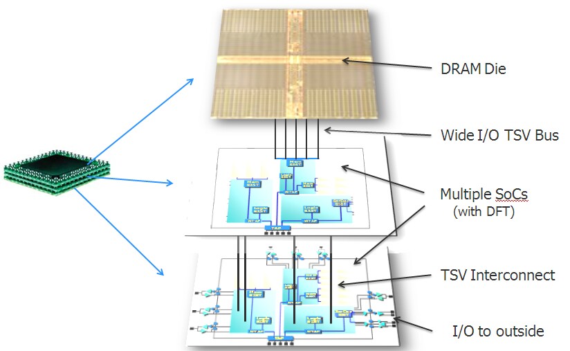
3D integration continues to receive considerable attention due to its envisioned potential to alleviate or reduce performance limitations in continued CMOS scaling
Details on 3D Processing Issues
 Effect of Etch Rate on Scalloping During Bosch Etching – ITRI
ITRI discussed their Bosch Etching process in detail. In general, the higher the etch rates the larger the scallops; for 1μm-dia TSVs, the effect of etch rate on the scallop is very small and the scalloping ranges from 57 nm to 83 nm (etch rate 1.7μm/min – 2.13μm/min); for 10μm-dia TSVs, the scalloping ranges from 107 nm to 278 nm (etch rate 3.5μm/min – 5.8μm/min), for 20μm-dia TSVs, scalloping is sizable ranging from 93 nm to 225 nm (for etch rate 4.2μm/min – 8.8μm/min); for 30μm-dia TSVs scalloping is significant, ranging from 97 nm to 258 nm (etch rate 4.6μm/min – 9.5μm/min); and for 50μm dia TSVs scallop is large ranging from 99 nm to 235 nm (etch rate 5.2μm/min – 11μm/min).
ITRI lists the following issues to be considered for high quality etching:
Impact of Slurry in Cu CMP – ITRI
ITRI discusses the minimization of dishing during the removal of thick Cu plating overburden due to filling TSVs and backside isolation oxide CMP for TSV Cu exposure. In order to obtain a minimum Cu dishing on the TSV region, proper selection of Cu slurries and a  two-step Cu polishing process was developed. The bulk of Cu is removed with the slurry of high Cu removal rate and then the Cu surface is planarized with the slurry of high Cu passivation capability at the second step. The Cu dishing can be improved up to 97% for the 10μm-diameter TSVs on a 300 mm wafer. They reached the following conclusions:
1. For Cu slurry selections for the wafer front side Cu CMP for TSVs and RDLs, the slurries of high removal rate should go along with that of high passivation capability to reduce the metal dishing. Using the slurry with high Cu removal rate to remove the thick Cu overburden on the field and changing to the slurry with high Cu passivation capability to clean the remaining Cu tends to have a much less metal dishing.
2. The Cu plating performance affects the metal/oxide dishing/erosion after CMP. Minimizing metal recess or dimple right on the patterns after Cu plating is an important indicator for reducing dishing/erosion after CMP. For TSV plating, transferring from Cu recess to Cu protrusion will lead to a much smaller post-CMP metal dishing.
3. Wafer edge trimming procedure before temporary bonding and backside grinding reduces edge chipping for the subsequent processes. 0.5 mm edge trimming can eliminate the edge chipping issue for a thinned wafer.
4. For backside oxide CMP for TSV Cu exposure, low pressure  should be used to reduce edge chipping during processing.
Selection of Adhesive Materials for Temporary Bonding – ITRI
Most thin-wafer handling solutions are wafer-support-systems: the wafer to be thinned is temporarily bonded on a supporting wafer with an adhesive and thinned down to the required thickness to expose the through silicon vias TSVs. Thin-wafer handling systems can be classified by the five material solutions [Brewer Science(BSI), 3M, TOK, DuPont and Thin Materials (T-MAT),] available through equipment vendors such as EVG, Suss and TOK.
The different material vendors provide various temporary bonding and de-bonding methods which significantly influence the material selection, equipment in demand and choice of silicon vs glass carrier. De-bonding processes involve various release methods including : (a) mechanical (TMAT), (b) thermal (BSI), (c) solvent (BSI, TOK), and (d) laser (3M, DuPont). A transparent glass wafer is required to serve as the carrier for UV cure and laser release which costs more than a normal Si carrier.
ITRI has shared the following conclusions:
1. Wafer thinning and PECVD-SiO2 deposition are the most critical steps for backside processes in thin-wafer handling making it only necessary to qualify an adhesive for these two conditions.
2. Backside polymer isolation is suggested to replace the backside PECVD SiO2 step (where possible) to alleviate thin-wafer processing issues.
3. /span>No obvious change or de-lamination occurred in all the chemical resistance tests for the different adhesive options.
4. The TTV performance of composite wafers with thinner adhesive has been found to be much better than that with thicker adhesive (100μm. Good TTV control for thicker adhesive still has to be developed.
Wafer thinning and back side processing  – IMEC
 The temporary bonding approach followed by IMEC is based on Brewer Science WaferBond  HT-10.10. After the HT 10.10 layer shows an average thickness of 16.2μm and a thickness variation of about 1μm across a 300 mm wafer. The wafer is thinned down by back grinding to a thickness typically leaving 57μm Si remaining for a TSV depth of 50μm. The total thickness variation (TTV) of the thin wafer after grinding is in the range of 1.6μm across a 300 mm wafer.
After thinning, an isotropic dry recess etch process reveals the TSVs while keeping the Cu protected in the oxide liner. The presence of the oxide liner prevents Cu oxidation that could occur during subsequent steps of the process flow. Without any CMP step during nail reveal, the TSV depth variation of about 1μm across the device wafers is measured by high resolution profilometry.
After nail reveal, a thermally compatible low temperature nitride passivation layer is deposited below 200°C. This passivation layer prevents Cu diffusion through the thin wafer to the FEOL active layers when redistribution layers or microbumps are processed on the backside prior to stacking. A nitride layer was been selected over an oxide layer based on the barrier properties of the 2 materials.
Metrology and Inspection During Bonding and Thinning – IMEC
For the in-line monitoring of the 3D wafers in the bonding and thinning module IMEC has examined the SPARK platform from NandaTech which has both brightfield and darkfield inspection capabilities.
There are several key metrology and inspection (M and I) challenges that need to be solved for successful 3D stacking of dies. The most critical steps have been identified to be TSV depth control, glue layer defects and control of the grinding process.
In the TSV module the critical metrology needs are measurements of via depth during etch and also detection of voids after via fill. If there are any depth variations over the wafer it translates to TSV height variations and this can become important during the grinding procedure. This depth variation should be feed-forwarded to the grinder so that the grinding can stop at a safe distance from the TSVs.
During the bonding of the device wafer to the carrier, glue layer defects larger than a few microns become critical. If these glue layer defects are not detected pre-thinning they propagate to the device wafer. Therefore, it is equally important to have the right in-line metrology to detect defects after  bonding which would indicate the presence of glue layer defects.
 During grinding it is absolutely vital to the residual Si thickness above the TSVs so that the TSVs are not prematurely exposed. The basic idea is to use a certain wavelength which will only partially penetrate the Si layer (i.e. lambda= 650 to 750 nm penetrates 1.5μm to 3.5μm) and then scan the wafer. If there is a TSV buried deeper than 3.5μm it won’t be scattering light. A map of residual Si thickness above the TSV can be generated from the image.
A proper feed-forward and a feedback system is necessary between the TSV, Bonding  and Thinning modules to compensate for process  variations.
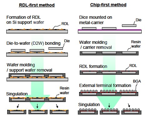
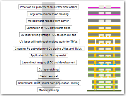
Wafer Level Molding for 3D Components – Samsung
Wafer molding is carried out in the chip-to-wafer process to ensure suitable levels of mechanical strength are reached. The key to wafer level mold processing is the reduction of warpage.
Samsung has studied material issues  optimized the wafer molding process to reduce warpage.  CTE mismatch between 50um thinned wafer and mold compounds is the primary challenge.  Test vehicles (bottom wafers, top chips) were fabricated on 300 mm wafers. A top chip of 8×8 mm2 size was designed and the bottom chip (including TSVs) was designed to a 12×12 mm2 size with 50um thickness. Before wafer molding, a supporting carrier was attached to the backside of the bottom wafer for wafer processing, backside via exposure and pad finishing. The top chips were then stacked on the wafer. After molding, the carrier wafer was detached and diced. The molded unit device’s warpage after dicing was measured by shadow moiré from room temperature to 240°C.
Molding material modulus, CTE, mold thickness and top chip thickness appear to be the parameters that drive the results. The size of the top chip was the dominant factor for warpage.  Warpage variation was mainly found at the overhang area where no top chip is present, which meant that the mold CTE mismatch was worse than inside the top chip area. Thus, a narrow overhang design is important for wafer molding.
Mold compound composition also had a strong influence on warpage as shown in the table below.
Conclusions include:
1.       Warpage decreased with increasing bottom chip thickness, and smaller chip size. This was directly related to the stresses encountered by the CTE mismatch between the mold material and silicon chip.
2.       Warpage decreased by decreasing the CTE and modulus of the mold material. Low modulus levels decreased the overall stiffness of the package, which is not desirable given that thin wafers need to be manufactured for the TSVs (usually manufactured to under 100μm depth). The minimum modulus values vary according to the packaging process and infrastructure, which is why careful selection of this value is required.
3.       Warpage levels can vary for the same mold material type depending on the filler content and resin type. By studying the effects of changing the filler content, it was found that decreasing this quantity improved warpage, as well as affecting the package reliability. The amount of shrinkage during curing of the resin also affected the stress levels in the mold material, and hence the warpage levels as well.
4.       Additional research is required to reduce warpage levels at room and high temperature to 40μm and achieve the required reliability levels. Package materials needs more investigation.
For all the latest on 3D IC and advanced packaging stay linked to IFTLE…..
We are trying the address the typo errors in this blog. Please be patient while we try to locate the cause of these errors ! 

IFTLE 54 2011 ECTC and Glass Interposers

Greater than 1000 attendees enjoyed the 2011 Electronic Component Technology Conference [ECTC] in Orlando FL. 342 of 641 submitted abstracts were selected by the program committee for presentation.

The technical focus continued to be on 3D integration which included  6 sessions and several dozen poster presentations. There were also a large number of submissions dealing with electromigration, the issues and reliability of fine pitch 3D micro joints, and numerous new advanced packaging proposals. We will begin by looking at TSMC and Ga Tech presentations on glass interposers and take a look at the other topics in the following weeks.

Glass Interposers

Glass is being examined as  a low cost alternative to the Si interposer. Compared to organic substrates ( ca 15 ppm), glass (3.2-9 ppm) has better CTE match to Si (2.3 ppm). Glass also exhibits excellent surface flatness, dimensional stability, high electrical resistivity and the availability in thin and large panels. The main challenges for glass interposers include:

– the ability to form ultrafine pitch TSV at high speed
– thermo-mechanical reliability of copper filled TSVs in glass
– thermal conductivity of glass (Si>glass>PWB)

Although the fracture strength of a defect-free glass is high, it decreases dramatically with any surface or bulk defects, which could be caused by processes such as etching, cutting, drilling, or metal deposition.

TSMC reported on test interposers which consisted of 100 um diameter TSV drilled in 360 um thick glass substrates on 200 – 500 um pitch. The test structures had 1,521 I/O in area array on a 40 x40 mm substrate.

They found that glass fracture strength decreases with decreasing TSV pitch. Higher via density leads to less cross section area and lower strength is observed. Data scatter is reportedly  due to structural defect s inherent in the glass after processing. They found that coating the glass on both sides with a “thin film material” (which appears to be PI) resulted in marginal improvements (10-20%) in glass fracture strength.
 ANSYS modeling was employed to simulate the material deformation for stress and strain analysis when the package is simulated under temperature excursion. A flip chip BGA with BT substrate was modeled for comparison purposes. Solder material, die thickness, glass size, glass thickness, via diameter, via pitch, PI coating thickness and CTE of glass were all examined as variables. When replacing the BT laminate with glass ( CTE of 8..3 ppm) the deformation of the package increases from 0.15 to 0.27 mm due to the larger CTE mismatch between substrate and PCB. Due to reduced CTE mismatch between die and glass, the maximum stress is reduced by approximately 38% when compared to the organic substrate. The most significant factor appears to be die thickness. Thick Si die introduce higher stress on glass substrate, owing to its increased rigidity which restricts the glass and/or die from deforming to relieve the stress. The CTE of the glass is also important since higher CTE glass induces higher stress to the die. They found that a medium CTE (ca. 8.3 ppm) glass is better for lower die stress.
The substrate serves as an interposer between low CTE Si die and high CTE PCB. Glass with higher CTE reduces BGA balls stress but is harmful to the Si die and vise versa. Overall, from the TSMC simulations, the medium CTE glass substrate at around 8.3 ppm is demonstrated as the optimal choice for the package structure. Some of the other factors, such as glass thickness, via diameter and PI thickness do not seem to play a significant role to affect the stress of the die, BGA ball or glass.
A Georgia Tech PRC consortium is also looking at glass as an interposer candidate . The glass substrates (either borosilicate [CTE = 3.8 ppm]or “high CTE” [8.5 ppm] glass) are 180 um thick with 15 um thick polymeric coatings on top and bottom similar to the TSMC construction. The 30 um TSV are either filled or conformal. Panel sizes are currently 150 mm.

The conformal TSV exhibited similar electrical performance as the filled TSV but are expected to show better thermo-mechanical reliability behavior. Stresses in the polymer layers are higher for thicker layers as expected.
Electrical properties of the glass interposer were extracted from measured and simulated data on ring resonators [dielectric constant ~ 4.8 and loss tangent ~ 0.002 up to 19.4 GHz. Low insertion loss of less than 0.15 dB at 9GHz was measured for the TPVs in the thin glass interposer.
For all the latest in 3D IC and advanced packaging stay linked to Insights From the Leading Edgeâ??¦

IFTLE 54 2011 ECTC and Glass Interposers

Greater than 1000 attendees enjoyed the 2011 Electronic Component Technology Conference [ECTC] in Orlando FL. 342 of 641 submitted abstracts were selected by the program committee for presentation.

The technical focus continued to be on 3D integration which included  6 sessions and several dozen poster presentations. There were also a large number of submissions dealing with electromigration, the issues and reliability of fine pitch 3D micro joints, and numerous new advanced packaging proposals. We will begin by looking at TSMC and Ga Tech presentations on glass interposers and take a look at the other topics in the following weeks.

Glass Interposers

Glass is being examined as  a low cost alternative to the Si interposer. Compared to organic substrates ( ca 15 ppm), glass (3.2-9 ppm) has better CTE match to Si (2.3 ppm). Glass also exhibits excellent surface flatness, dimensional stability, high electrical resistivity and the availability in thin and large panels. The main challenges for glass interposers include:

– the ability to form ultrafine pitch TSV at high speed
– thermo-mechanical reliability of copper filled TSVs in glass
– thermal conductivity of glass (Si>glass>PWB)

Although the fracture strength of a defect-free glass is high, it decreases dramatically with any surface or bulk defects, which could be caused by processes such as etching, cutting, drilling, or metal deposition.

TSMC reported on test interposers which consisted of 100 um diameter TSV drilled in 360 um thick glass substrates on 200 â???? 500 um pitch. The test structures had 1,521 I/O in area array on a 40 x40 mm substrate.

They found that glass fracture strength decreases with decreasing TSV pitch. Higher via density leads to less cross section area and lower strength is observed. Data scatter is reportedly  due to structural defect s inherent in the glass after processing. They found that coating the glass on both sides with a â????thin film materialâ???? (which appears to be PI) resulted in marginal improvements (10-20%) in glass fracture strength.
 ANSYS modeling was employed to simulate the material deformation for stress and strain analysis when the package is simulated under temperature excursion. A flip chip BGA with BT substrate was modeled for comparison purposes. Solder material, die thickness, glass size, glass thickness, via diameter, via pitch, PI coating thickness and CTE of glass were all examined as variables. When replacing the BT laminate with glass ( CTE of 8..3 ppm) the deformation of the package increases from 0.15 to 0.27 mm due to the larger CTE mismatch between substrate and PCB. Due to reduced CTE mismatch between die and glass, the maximum stress is reduced by approximately 38% when compared to the organic substrate. The most significant factor appears to be die thickness. Thick Si die introduce higher stress on glass substrate, owing to its increased rigidity which restricts the glass and/or die from deforming to relieve the stress. The CTE of the glass is also important since higher CTE glass induces higher stress to the die. They found that a medium CTE (ca. 8.3 ppm) glass is better for lower die stress.
The substrate serves as an interposer between low CTE Si die and high CTE PCB. Glass with higher CTE reduces BGA balls stress but is harmful to the Si die and vise versa. Overall, from the TSMC simulations, the medium CTE glass substrate at around 8.3 ppm is demonstrated as the optimal choice for the package structure. Some of the other factors, such as glass thickness, via diameter and PI thickness do not seem to play a significant role to affect the stress of the die, BGA ball or glass.
A Georgia Tech PRC consortium is also looking at glass as an interposer candidate . The glass substrates (either borosilicate [CTE = 3.8 ppm]or â????high CTEâ???? [8.5 ppm] glass) are 180 um thick with 15 um thick polymeric coatings on top and bottom similar to the TSMC construction. The 30 um TSV are either filled or conformal. Panel sizes are currently 150 mm.

The conformal TSV exhibited similar electrical performance as the filled TSV but are expected to show better thermo-mechanical reliability behavior. Stresses in the polymer layers are higher for thicker layers as expected.
Electrical properties of the glass interposer were extracted from measured and simulated data on ring resonators [dielectric constant ~ 4.8 and loss tangent ~ 0.002 up to 19.4 GHz. Low insertion loss of less than 0.15 dB at 9GHz was measured for the TPVs in the thin glass interposer.
For all the latest in 3D IC and advanced packaging stay linked to Insights From the Leading Edgeâ??¦

IFTLE 53 One Year Later?. Amkor / TI High Density Copper Pillar Bump Technology

In late June 2010 Amkor and TI announced that they had qualified and begun production of the industry’s first fine pitch copper pillar flip chip packages – shrinking bump pitch up to 300 percent compared to then current solder bump flip chip technology [see IFTLE 23, “Xilinx 28 nm Multidie FPGA, Copper Pillar Advances at Amkor â??¦”]


Very little technical detail was released at that time, presumably because of the rumored exclusivity TI was given as part of the joint development program. Full technical details were to be withheld a year till the 2011 ECTC conference, which just occurred this past week. We’ll be covering the overall ECTC technical content over the next few weeks, but I first wanted to focus on the Amkor / TI paper “Next Generation Fine Pitch Cu Pillar Technology – Enabling next generation Silicon Nodes” since we have all been waiting a year for the details which were presented by Curtis Zwenger (Amkor) and Mark Gerber (TI).

Flip chip technology has traditionally been driven by electrical performance and package miniaturization, with application processors being the primary drivers for mobile phone applications. Traditional solder or Cu Pillar interconnect pitches have been 150um to 200um for both low and high end flip chip applications. Today wafers are routinely bumped at 140 – 180 um pitch with 90 um solder balls in area array. Advanced silicon nodes create challenges to fine pitch (less than 100 um) flip chip interconnects and the corresponding substrate technology. Use of low-k dielectrics, thinner ICs, and package warpage are challenges.

Migrating from wire bond interconnects to area array flip chip requires a redistribution layer be added to the device to provide the required interconnection pattern. Fine pitch flip chip is compatible with existing in-line and staggered wire bond pad patterns, avoiding the cost for redistribution of the circuit on the die. Amkor claims that 80 percent of their internal studies on converting existing area array flip chip designs to fine pitch designs resulted in a lower cost substrate due to metal layer count reduction and/or body size reduction.

Fine Pitch Cu Pillar Test Vehicle
The qualification vehicle was a 559 bump chip on 50 um pitch and a 0.4 mm BGA array coming off the substrate ( 12 – 14 mm PoP body size).

Qualified design dimensions are shown in the figure below. Composition of the solder cap and the Pb free solder were not identified.

The primary process development challenge centered on the flip chip attach and bonding processes. For Cu Pillar flip chip with pitches less than 100um, the placement accuracy of the die to substrate is critical to help ensure a high yielding manufacturing process. Amkor found that thermal compression bonding was best suited for fine pitch copper pillar products. Thermal compression bonding, used in conjunction with a pre applied underfill (NCP = non conductive paste). The process flow is shown in the figure below.

It is important to control the height of the die in relation to the substrate. Pillar height, substrate capture pad height, and die thickness must be controlled to help ensure a stable process. For an over bonded Cu pillar die the solder cap can be squeezed out the sides of the joint causing solder shorts between the pillars.

The new fine pitch packages were put through standard JEDEC MSL L3 260 ºC un-biased package reliability tests including temperature and humidity, unbiased HAST, temperature cycle level B and high temperature storage tests as well as board-level reliability (BLR) testing (drop and temperature cycle) and biased component-level (CLR) reliability testing.


Rumors are that Amkor is adding additional fine pitch Cu Pillar capacity for TI and that the process is being transferred to TI who will be putting additional capacity in place for some of their own products. TI has indicated that they are open to licensing the fine pitch Cu pillar technology to others.


For all the latest on 3D IC and advanced packaging stay linked to IFTLEâ??¦â??¦â??¦â??¦..